Abstract
Scanning electron microscopy (SEM) is a common method for the analysis of painting micro-samples. The high resolution of this technique offers precise surface analysis and can be coupled with an energy-dispersive spectrometer for the acquisition of the elemental composition. For light microscopy and SEM analysis, the painting micro-samples are commonly prepared as cross-sections, where the micro-sample positioned on the side is embedded in a resin. Therefore, the sequence of its layers is exposed after the cross-section is polished. In common cases outside of cultural heritage, a conductive layer is applied on the polished side, but in this field, the measurements are mostly done in low-vacuum SEM (LV-SEM). Although the charging effect is reduced in LV-SEM, it can still occur, and can hardly be prevented even with carbon tape or paint. This work presents two conductive cross-section preparation methods for non-conductive samples, which reduce charging effects without impairing the sample integrity.
Subject terms: Characterization and analytical techniques, Imaging techniques, Scanning electron microscopy, Solid Earth sciences
Introduction
Scanning electron microscopy (SEM) is a widely used analytical technique in several fields, such as engineering1, forensics1–3, geology4, biology5,6 and medicine7,8. In the field of cultural heritage, the SEM analysis is an essential part of the examination of painting micro-sample cross-sections9–14. However, the analysis of such samples is complex due to their non-conductivity, uniqueness, and both structural and material heterogeneity.
A SEM measurement is carried out in a vacuum chamber, where a convergent electron beam, created by electromagnetic lenses to focus and remove aberrations of the image, hits the surface of the sample15. The interaction of the beam with the sample surface produces several signals. The outputs of these signals can be interpreted with different detectors and give various information, such as the chemical composition (Energy-Dispersive Spectroscopy—EDS), which is mostly used in the study of painting micro-samples, the present phases (Back-Scattered Electrons—BSE), the texture/topography (Secondary Electrons—SE), the crystalline structure and the orientation of particles. The detailed principles are discussed elsewhere15,16.
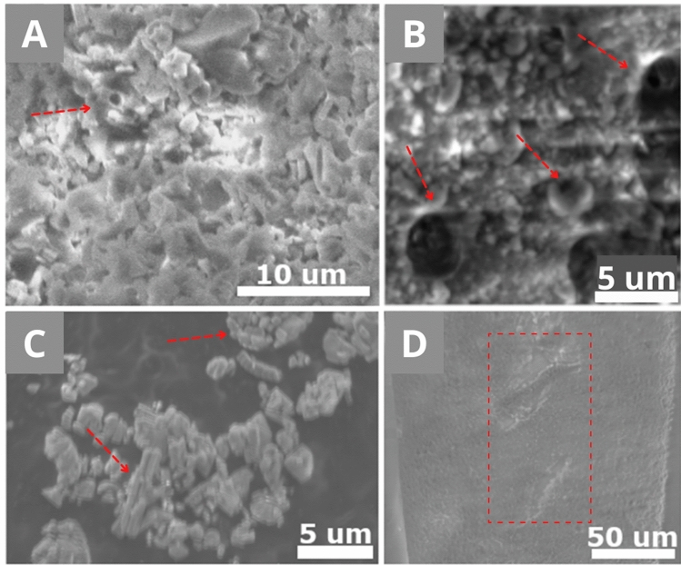
For the measurement, a voltage is applied for accelerating the electrons15.When the accelerated electrons hit gas molecules still present in the vacuum chamber, it shortens their mean free path and influences the image quality negatively15. High-pressure environments have fewer gas molecules and are preferred, but a charging effect may occur on non-conductive samples when the charge of the electrons is not balanced17. The charging effect is a concentration of electrons at a specific place, creating uneven brightness (Fig. 1A), bright lines (Fig. 1B), image distortions (Fig. 1C) and/or a lack of a stereoscopic sense (Fig. 1D). These effects could indirectly influence the measurement of the chemical composition (bad/unclear positioning).
Figure 1.
MIRA3 XMU SEM-SE images of charging effects. (A) and (C) are chalk powder composed of calcareous nannofossils; (B) and (D) show the surface of a foraminifera Uvigerina sp. The red arrows and frame show the material planned to be studied. (A) Uneven brightness creates bright spots and too dark areas, hiding features of the sample. (B) Bright lines created by charging do not allow the interpretation of the homogeneity of the surface. (C) Image distortion modifies the visualisation of the sample and renders its interpretation impossible. (D) Lack of stereoscopic sense hinders the topographical analysis and shape observation.
The preparation of samples is varied18, but the most common is to use directly the sample as it is19–21 or to prepare a thin/thick section18. To avoid the charging effect, both methods require either coating the non-conductive samples or using a low-vacuum mode8. A coating is an ultra-thin conductive layer of metallic molecules (Au, Pt) or carbon applied on the surface of the sample or its cross-section22–24. It equalises the charge on the whole surface, where the excess of electrons flows away from the sample1,25–27. The sample coating is the most common way to avoid charging in a high-vacuum mode28. In the field of cultural heritage, the coating is often undesired because of the multi-technical approach9–12,14. The coating can influence surface characteristics, e. g. impair the colours of the sample29 and/or the elemental composition of the sample, which are important issues regarding painting micro-samples. Moreover, the removal of such layers is done mechanically or using chemicals which can strongly interact and destroy the surface of the sample26,27,29–34 for further studies.
In technical fields, using a conductive resin, such as an epoxy or acrylic resin mixed with an additive conductive material, is common35. But these resins are mostly coloured, which impairs the light microscopical visualisation of the cross-section prior to the SEM analysis36. The use of conductive paint and/or tape can be helpful in some cases37, but cannot replace a proper coating or the use of a conductive resin, and does not work on large non-conductive samples.
The analysis of non-conductive samples which cannot be coated is mainly done in a low-vacuum environment (LV-SEM)15,38 or an environmental SEM (ESEM)39. The low vacuum reduces the charging effect, but also lowers the image resolution. In this case, the gas molecules still present in the vacuum chamber, due to the low vacuum, shorten the free mean path of the electron by producing ions that neutralise the excess of electrons and reduce the charging15. It should be noted that the components of a sample can have various interactions with the electrons, such as outgas and evaporation, and particularly organic matter and wet matter (coal, organic material, swelling clays)40. An increasing chamber contamination of these materials can affect the vacuum, thus impacting the charging effect41.
The cross-section preparation is common for the morphological and chemical analysis of micro-samples from paintings42–47. The information gained from a painting cross-section can be about the painting technique, the layering, the pigments, the grains distribution, the porosity and cracks, the colour, and the binders47–49, which is important for conservation, the appropriate restoration and the art comprehension13,50–54.
A cross-section is the embedding of a sample in a material, such as a resin54. The choice of the resin, the encapsulation type, and the polishing can have a serious impact on the sample and measurement. They should be, therefore, chosen carefully55,56.
The resin should be chosen according to its characteristics57,58, the planned analyses and the sample type. Among the characteristics are the curing temperature59 and time, transparency60, fluorescence61, shrinkage59,62,63, hardness, viscosity58,64 and additives60,61,65–67. Some authors have used bioplastic in the last years, but there are not enough studies on their ageing available to assess the possibility of a long-term use68. Khandekar69, Derrick et al.64 and Waentig70 addressed most of the issues about the choice of the resin and the preparation material according to the sample type. A specific requirement of painting micro-samples is to use a clear and low temperature curing resin, which discards the coloured conductive resin. A low temperature curing resin prevents the evaporation or molecular modifications of the organic components often present in painting samples, but also thermal chemical reactions between some components, thus, morphological changes. There are different types of resin encapsulations62,63,65,66, as well as sample fixation methods, which are discussed elsewhere67.
In this work, the aim was to develop a resin cross-section preparation for non-conductive samples to reduce the charging effect without impairing the sample characteristics (colour, morphology, chemical composition) with any coating or coloured resin. The suggested preparation procedures are a combination of established methods of painting micro-sample preparation, and the procedures aim to be time, cost and results effective.
Materials and methods
Samples
The chosen samples (Table 1) represent a fully non-conductive material (MS1, MS2) and a partially conductive one (MS3, RS1, RS2) (Table 1). MS1 and MS2 are model samples made of pure chalk and an organic binder. MS3 is a partially conductive model sample. A restorer prepared the model samples to improve the comparison with historical painting micro-samples. MS3 contains a layer of yellow earth mixed with an egg yolk (tempera technique) with iron particles which make it partially conductive on top of chalk, and a rabbit skin glue non-conductive layer.
Table 1.
Different samples regarding their porosity and conductivity were used for the experiment. MS1 and MS2 are not conductive, while MS3, RS1 and RS2 have some metallic particles (iron) in their pigmented layers.
| Sample | Pigment | Preparatory layer | Binder | Number of Layers |
|---|---|---|---|---|
| MS1 | – | Chalk | RSG | 1 |
| MS2 | – | Chalk | LO | 1 |
| MS3 | Yellow earth | Chalk | RSG + T | 2 |
| RS1 | Green earth | Chalk | Oil U + T | 3 |
| RS2 | Yellow and green earth | Mortar | Carbonaceous | 4 |
MS: Model sample; RS: Real sample; RSG: Rabbit skin glue; LO: Linseed oil; T: Tempera; U: Unknown.
RS1 is a real historical sample with a top green earth tempera layer and a chalk preparatory layer with an unknown oil binder. RS2 is also a real sample of a wall painting, with green and yellow earth layers on top of two carbonaceous preparatory layers. All samples are smaller than 1 mm in all directions.
Epoxy resins
The materials used for this study are relatively easy to find and established for a cross-section preparation. Various types of epoxy resins were used for the preparation55,71. EpoFix (Struers, DK) was used for the direct embedding of all samples and the reference non-conductive preparation. It is a transparent dual-component cold mounting resin combining an epoxy resin with a hardener. Its curing time is approximately 12 h. It is a relatively common type of resin already used for painting micro-samples embedding64.
PolyFast and LevoFast (Struers, DK) are hot mounting powder resins. PolyFast is a conductive resin used for the Preparation A, and LevoFast is a particularly hard resin used for the polishing holder designed for this work.
The Reference and Preparation A were prepared in a round plastic mould (Struers, DK), which is made for a vacuum impregnation chamber (CitoVac, Struers, DK) to help remove bubbles to increase the stability and hardness of the resin. To fix the positioning of the sample, plastic clips were used.
For the other preparations, two silicone ice cube trays of 1 cm × 1 cm × 1 cm and 1 cm × 1.5 cm × 1.5 cm were tested. The two trays had different silicone textures. The small one had a porous texture, giving a final milky appearance of the resin, while the large tray gave a transparent final aspect. The small cubes better fitted the size of our micro-samples and made the positioning easier. The larger cubes were easier to handle and could be useful for large or long samples. Even though the transparency of the cubes from the larger tray made it easier to observe the samples in the resin, the smaller silicon tray was harder and, thus, easier to handle, and the milky appearance was not hindering the polishing process. In our case, the smaller ice cube tray of 1 cm × 1 cm × 1 cm for the conductive preparation was more appropriate.
Instrumentation
The CitoPress-10 hot mounting press (Struers, DK) was used for the PolyFast and LevoFast resins.
A Leica EM ACE 600 high-vacuum coater was used for the application of a carbon coating of 30 nm in Preparation B.
The grinding and polishing of the cross-sections were done as described in Jaques and Zikmundová (unpublished). Before the sample was reached, the polishing mode was changed from wet to dry47.
The first observations of the cross-sections were made under the Stemi 2000-C and Stemi 508 stereomicroscopes (Zeiss, DE) and a Reichert microscope (Reichert Technologies, US) coupled to an Axiocam ERc 5 s (Zeiss, DE).
The scanning electron microscope used for this study is a MIRA3 XMU (Tescan, CZ). Both the high-vacuum (5 mbar to 9 × 10⁻⁵ mbar) mode and the low-vacuum (0.07 mbar to 5 mbar) mode with a secondary electron detector (LVSTD mode) were used.
Cross-section preparation
The non-conductive cross-sections were prepared with the 5 samples (Table 1) as references (Table 2). Then two conductive preparations (A and B) were developed (Table 2).
Table 2.
Overview of the preparation methods.
| Reference | Conductive A | Conductive B | |
|---|---|---|---|
| Embedding type5 | Capsule + flat | Slotted-capsuled block | Flat |
| Resin | EpoFix | PolyFast + EpoFix | EpoFix |
| Mould [cm] | 2 × 1 ø | 1.5 × 1.5 × 1.5 | 2 × 1 ø | 1 × 1 × 1 |
| Conductive material | – | PolyFast + Cu-tape | 30 nm Carbon-coating |
| Preparation time [h] | 12 | 7 | 12 |
Reference preparations
The reference preparations (Fig. 2) are non-conductive, except for the specific conductive particles of the sample (MS3, RS1, RS2). The capsule reference preparation was prepared by positioning the samples and then adding the resin through the CitoVac device. The CitoVac is used to pour the resin via a plastic tube onto the micro-sample placed in a circular mould in a vacuum chamber. This technique offers cured resin with less to no bubbles and better penetration of the resin in the sample. The capsule embedding had a curing time of approximately 12 h regarding the dual-component epoxy. 12.5 g of the EpoFix per 1.5 g of the hardener were used and gently poured on top of the sample. The samples were fixed using plastic clips, which, however, moved, and had to be repositioned. A second reference preparation was made using a flat embedding with the same samples. The mould was 1.5 cm × 1.5 cm × 1.5 cm to ease manual polishing without the polishing holder. Depending on the size of the sample, it can also be useful to have a larger mould size. The sample was positioned on the surface of the already dried resin filling half of the mould. A drop of the EpoFix was applied on top of the sample and left for approximately 30 min. This lightly fixed the sample and avoided drifting or floating. Then the rest of the resin was gently poured on top. The CitoVac was not used in this case. The flat embedding gave better results for the orientation, even though its preparation is slightly more demanding. After the curing time, the embedded samples were polished with the Tegramin in an automatic mode.
Figure 2.
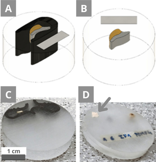
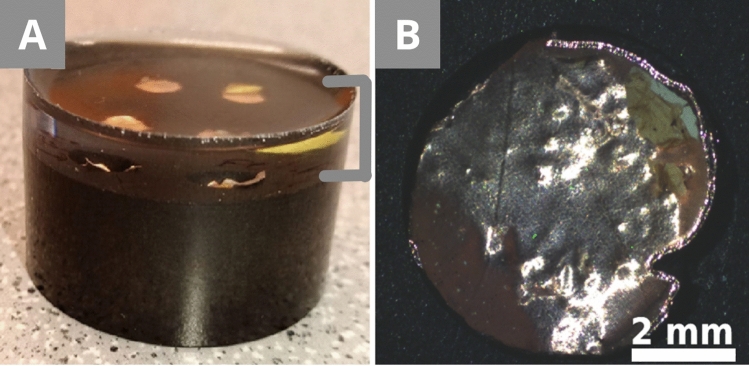
Reference preparation with the fixing clips as (A) a scheme and (C) in reality, and without the clips (B) as a scheme and (D) in reality. The grey arrow shows a part of a sample that floated to the surface of the resin (for detail see Fig. 6). The cross-section diameter is 3 cm.
Conductive preparation A
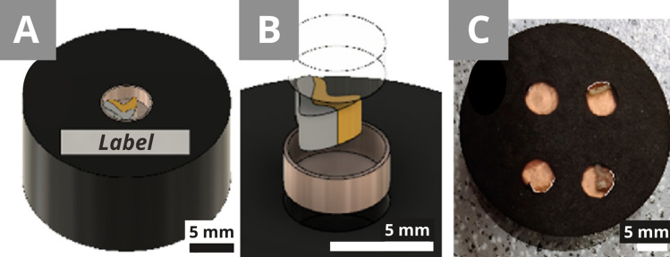
Slotted-capsule embedding was chosen because the two-step preparation (hot resin then cold resin) created with small holes helps the sample positioning and partially avoids floating and drifting. The preparation using the CitoPress was done according to its instructions. This step took approximately 10 min. Four flat bottom holes of 5 mm in diameter and 2 mm deep were drilled in the PolyFast block (Fig. 3C). If the samples have a similar height (perpendicular to the bottom of the hole), more can be put in the same block, but it can make it more difficult to get an interesting surface for all of them while polishing. Therefore, a maximum of two samples of the same height in one resin block is recommended. A batch of blocks can be prepared in advance, either with or without the holes. The depth of the holes can also vary according to the size of the samples. The copper tape was added to the bottom and around the hole. One sample per hole was fixed and put into tight contact with the copper tape (Fig. 3B). The hole was finally filled with the EpoFix (Fig. 3B), and the curing was shorter due to the small amount of the resin. The cross-sections were then polished with the Tegramin.
Figure 3.
(A) Design of the conductive preparation A (3 cm in diameter). (B) A scheme of the different parts: the black PolyFast, the copper tape (bronze), the layered sample (orange/grey) and finally the transparent EpoFix. (C) The real preparation of a PolyFast conductive block with each of the 4 samples in a different hole with a copper tape.
Conductive preparation B
For the flat-embedding preparation, half of the silicone mould of 1 cm × 1 cm × 1 cm was filled with the EpoFix and left to cure similarly to the flat reference preparation (Fig. 4A). The surface of the lower part of the resin was coated with a 30 nm carbon layer with a Leica coating device (Fig. 4C). The sample was then put on top with a tiny drop of resin or a quick-dry gel glue (Fig. 4D). A high viscosity material, such as the gel glue, prevents its spreading on the resin surface and in/on the sample. Only a small part of the bottom of the sample should be glued. The glue should not interfere between the coating layer and the sample. After a short curing time of the glue, a second carbon coating is done on top of the preparation (Fig. 4E). Finally, the second layer of the resin is added to fill the mould and fix the sample (Fig. 4F). A holder specifically designed for this experiment was used for polishing the cross-sections. The first polishing was wet (using water) and then just before getting to the sample, the mode was switched to a dry mode to prevent the disaggregation of the sample components. The pressure and speed of the rotation plate were also reduced to avoid deep scratches on the surface of the resin and its melting.
Figure 4.
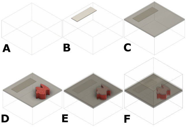
Preparation B scheme. (A) Cured EpoFix in 1/2 of the mould. (B) Label glued downwards. The label can also be added upwards after step (E). (C) The lower part of the resin is coated with carbon (grey). (D) The sample (red) is oriented on the resin ½ cube. (E) The surface of the sample (red) is coated with carbon (grey), which will connect with the first layer from step (C). (F) The rest of the mould is filled with the EpoFix and left for curing.
Polishing holder
Before the analysis, cross-sections must be polished to get a clear, smooth surface of the sample without the resin on top of it. Although round moulds are typical for cross-section preparation, they are not always of the best size or shape for the sample. The smaller cubes were chosen, which are common in cultural heritage sample preparation, with a manual polishing. The Tegramin automatic mode cannot be used for such cubes because of their shape and size that does not fit the device. The cubes are also rather small, which makes it more difficult to get a flat, smooth polished surface and avoid deep scratches. Therefore, it was decided to use the Tegramin for a certain standardisation of the preparation and to avoid user errors, such as uneven surfaces and deep scratches. A polishing holder was designed to fit the cubes into the Tegramin (Fig. 5A).
Figure 5.
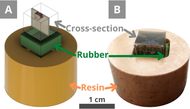
(A) Scheme of the holder with the LevoFast resin, a silicone rubber, and a cross-section (Fig. 4F) to be polished. (B) The achieved holder for the 1 cm × 1 cm × 1 cm cross-sections.
The holder was made of the LevoFast resin, composed of melamine, minerals, and glass fillers. It is a harder resin than EpoFix used for embedding and, thus, more resistant to polishing. This resin is hot mounting and was prepared using the CitoPress.
A square of 1 cm × 1 cm × 0.75 cm was drilled in the centre of the round piece, and a square silicone rubber with walls of a 2 mm thickness was introduced into it (Fig. 5). The silicone rubber fixes the cross-section, allowing only small movements of it. Also, the resin can shrink during curing, preventing the final shape to be a perfect cube, hence the silicon rubber.
Results and discussion
The preparation procedure of each method was evaluated according to the total time of the preparation, the ease of the preparation, and the visual assessment of the surface under the light and electron microscopes. The conductivity of the cross-sections prepared according to the Preparation A or B (Table 2) was evaluated in a visual comparison with the reference preparation cross-sections of a similar sample. The image quality based on the amount of charging and strength of the artefacts was evaluated during the imaging process.
Cross-section preparation
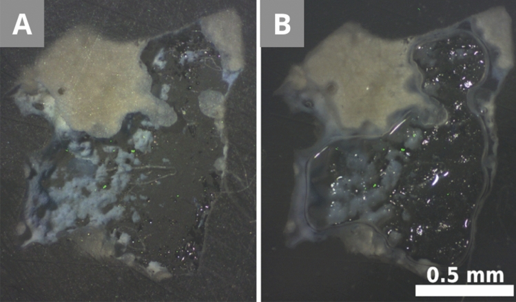
Preparation A (Fig. 3) needs the hot resin to be prepared in advance (appr. 8 min) and the holes to be drilled in the resin (appr. 5 min), but the curing time of the transparent EpoFix is reduced from 12 h to appr. 6 h thanks to the small amount needed. The hole helps positioning the sample with copper tape and a low amount of resin, which strongly reduces the floating and drifting of the sample compared to the reference preparation. The capsule embedding (Fig. 2) offers a one-step preparation without previous planning, but the amount of the curing resin increases the risk of sample misplacement even with plastic clips. These clips are useful for flat and rather large samples, but they reduce sample visibility and cannot be used for brittle, non-flat samples. Highly porous samples floated to the surface despite multiple repositioning during the hardening of the resin (12 h). Without the clips or any other fixing, the samples floated (Fig. 2D—grey arrow + Fig. 6). One of the reference samples drifted into a horizontal position (Fig. 6), instead of staying on its side to show the layering. In our case, the sample only contained a chalk layer, but with any other sample, most stratigraphic information would have been lost.
Figure 6.
Unfixed sample MS1 that floated during the curing of the resin, and the parts of it removed during the polishing. (A) The scratches on the resin and the sample surface are visible. (B) Most scratches disappear thanks to the application of a drop of water and a coverslip over the sample, which creates an even surface.
Preparation A reduces the manipulation of the sample (Fig. 7). The diameter and depth of the hole can be adapted to the size and shape of the sample. In our case, a diameter of 5 mm and a depth of 2 mm were used (Fig. 7A). However, the diameter was too large for our samples, which were between 1 and 3 mm long (Fig. 7B). The chosen depth was relatively advantageous for all samples.
Figure 7.
Preparation B. (A) Transparent resin fills the holes made in the conductive resin. This layer can be reduced to its minimum by filling only the holes. The thickness of the transparent layer of the cross-section (marked grey) and the conductive resin can be used for automatic polishing. (B) The sample is fixed with copper tape.
Under the microscope, scratches were visible on the surface of the cross-sections A. There was no visible difference in the depth of the scratches between the reference cross-sections and cross-sections A. These scratches occur due to the combination of coarse polishing particles and the pressure applied during the polishing steps (Fig. 6A). It could be visually attenuated by applying a drop of ethanol or water and a coverslip on top (Fig. 6B), but this technique is not recommended, as it can dissolve some components of the sample.
Preparation A has a quick curing time, but includes preparatory steps that need to be planned relatively in advance (drilling, two rounds of curing). It also needs two different resins (PolyFast, EpoFix). The thickness of the transparent resin can be measured (Fig. 7A) and used to set the parameters of the automatic polishing to protect the sample from being destroyed during the process. It helps change the polishing mode from wet to dry in time. The holder used to secure the cross-section while polishing them reduces uneven surface, deep scratches, and offers the possibility to set in the automatic mode the polishing time and pressure in the Tegramin. For manual polishing, the size of the holder offers a better hold of the cross-section for the users, which improves the polishing results. The main advantage of Preparation A is the possibility of preparing more samples simultaneously. In the case of preparing multiple samples, the amount of the PolyFast resin is reduced compared to a single sample preparation. Moreover, with all samples polished into a uniform height, there is no need to adapt the focus to each cross-section separately, which reduces the working time. Hence, one cross-section containing several micro-samples can reduce the preparation time, measurement time, and amount of material (i.e. embedding medium).
Preparation B (Fig. 4) also requires the first half of the EpoFix resin to be cured in advance and its surface coated with carbon (appr. 6–8 h). Both steps can be carried out in a batch and stored for later use. This preparation does not need any additional materials or procedures. Fixing the sample is the most sensitive part of the procedure, and it strongly influences the conductivity of the preparation, as the fixing medium acts as an insulator. The second coating needs to be connected to the first coating layer, and this carbon network should be in contact with the sample all around, but also with the SEM metallic holder to create an appropriate exit path for the electrons to avoid charging. The cross-section polishing becomes quicker and easier with the holder and the Tegramin. The pressure control of the Tegramin can also help reduce the scratches.
The capsule-embedding reference preparation was easy, quick, and cheap, and had only 2 steps (sample positioning, resin curing). The main issues of this preparation were the sample drifting during curing, the long curing time because of the relatively large amount of the resin, and the charging of the cross-section under the SEM beam. With the flat-embedding preparation, which was used for Preparation B, the positioning was easier, but there were three steps (resin curing, positioning, resin curing again) and it was also charging. Preparation A was the most stable and easiest for sample positioning.
Cross-section conductivity
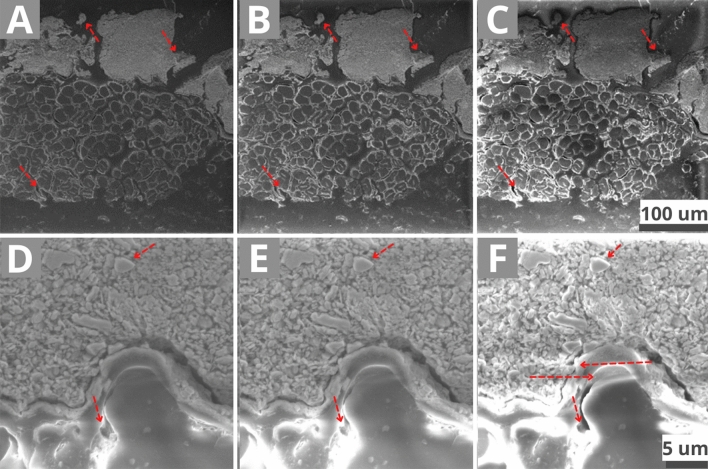
The charging of the cross-sections was visually assessed and marked from 0 to 3: 0 – no charging; 1—low charging and a relatively homogeneous image contrast Fig. 8A + 8D; 2—half of the components are charging, and some charging effects (Fig. 1) appear more consistently Fig. 8B + 8E; 3—more than ¾ of the components are charging, and charging effects are strongly occurring Fig. 8C + 8F. In Fig. 8C and 8F, a high over-exposition (electron concentration) of the materials can be observed, particularly of the fibres (organic), but also a darkening of the inorganic material rims, creating a contrast imbalance. The uneven brightness (Fig. 1A) of the material creates visual artefacts and hinders proper observation of the sample. From Fig. 8A–C and at higher magnification from 8D to 8F, a contrast gradation from homogeneous to inhomogeneous can be seen.
Figure 8.
RS1 reference at 10 kV average magnification (801 x) WD 14 mm (A) 50 Pa vacuum marked as 1—low charging. The image contrast is relatively homogeneous, and the image is relatively stable. (B) 20 Pa vacuum marked as 2—Medium charging. Some parts of the pictures are becoming bright or dark (red arrows), the image contrasts are less homogeneous, and the image is unstable. (C) 15 Pa vacuum marked as 3—High charging. Very bright or dark parts hiding details of the sample appear, the image contrast is inhomogeneous, and the image is highly unstable (drifting). The contrast manager cannot smooth the differences. RS1 reference at higher magnification (10 kx) (D) 50 Pa 1—low charging. Some parts are charging (organic and resin; uneven brightness (Fig. 1A), but the image quality stays acceptable. (E) 20 Pa 2—Medium charging. Most details are invisible due to the increasing uneven brightness and the contrast of the inorganic material increases (red arrows). The image drifting increases. (F) 15 Pa 3—High charging. The uneven brightness is now on all materials. Bright lines (horizontal arrows; Fig. 1B) and a blurred image can also be observed.
The reference preparation showed high charging (2–3) at 10 kV, but stabilised from 20 kV (2–1). A charging modification depending on the sample morphology occurred around 30 Pa. The homogeneous samples (MS1/2) had stable charging effects on their surface compared to the multi-layered ones (MS3, RS1/2 Fig. 8A), where the charging was high in localised areas (Fig. 8D—around organic fibres). The charging was reduced from 3 to 2, but was still present at any magnification (low 500 x; average 500 × to 3 kx; high 3 kx), and with any parameters and samples (1).
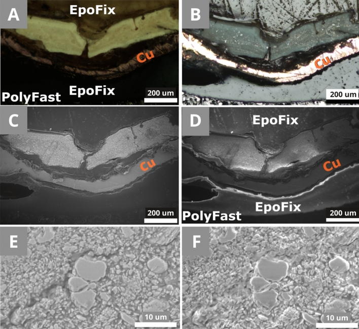
In Preparation A (Fig. 3), the sample is in direct contact with a conductive material. The copper tape (Cu) (Fig. 9A + 9B) is connected to the conductive resin, creating an exit path for the electrons. At 10 kV | 10 Pa and 15 Pa, the charging in the middle of the non-conductive resin was very high (3) at low magnification and slightly lower (2) at an average magnification. Almost no charging occurred at 10 kV | 50 Pa, even at a high magnification (1–0) (Fig. 9C), whereas in the reference preparation 0 charging effect was never reached. Both the homogeneous and the multi-layered samples had a charging decrease, 2 to 1, at 10 kV | 20 Pa (Fig. 9D). This preparation showed promising results, where the charging occurred only in the transparent resin area, but not around the sample or the copper tape. At a high magnification, the charging was reduced only where the sample was in direct contact with the conductive material (Fig. 9D). Even though, at a high magnification, the charging of the chalk ground decreases to a certain extent due to a vacuum increase (Fig. 9E + 9F). The sample needs to be in tight contact with the conductive component to effectively reduce the charging.
Figure 9.
RS1 in preparation A. (A) Bright light and (B) polarized light microscopic image. (C) SEM-SE image at 10 kV | 50 Pa and (D) at 10 kV | 20 Pa. (E) SEM-SE image at 10 kV | 50 Pa and (F) at 10 kV | 20 Pa at a higher magnification.
Preparation B (Fig. 4) was designed based on the observations made during Preparation A. The use of carbon sputtering for the coating fits the shape of the sample and surrounds it better than the copper tape (Fig. 10A). The direct contact between the conductive material and the sample was expected to be better than in the Preparation A. The coated surface of the resin (Fig. 4C) works as the exit path for the electrons from the cross-section to the metallic SEM holder. Similarly, in Preparation A, the charging was reduced where the sample was in direct contact with it. But the carbon layer was not even (Fig. 10B) and was disrupted during the sputtering mostly around the samples' edges and vertical surfaces. During the carbon sputtering, the vacuum can be chosen, as well as the theoretical thickness of the carbon layer. In our case, 30 nm thickness (relatively thick) was chosen for a low vacuum (around 2 Pa). With a lower vacuum, the sputtering was less precise and less even (Fig. 10C). The main problem of this preparation was the glue spreading between the sample and the carbon layer. Therefore, the sample was mostly not in contact with the first carbon layer anymore. The second coating disruption occurred due to the direction of the sputtering (the stage of the coating device can be tilted to improve the carbon deposition depending on the sample shape). Only one side of the sample was coated, and due to its uneven surface and morphology, the connection between the two carbon layers was not as good as expected. Consequently, the charging was not appropriately reduced.
Figure 10.
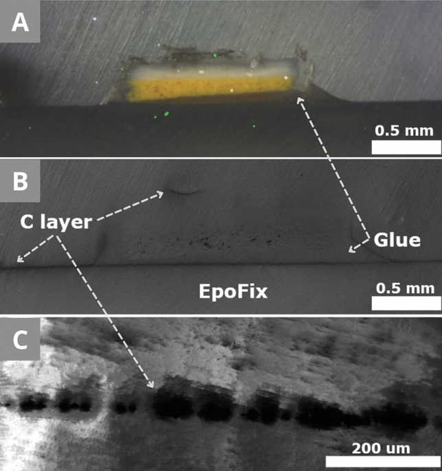
Preparation B of MS2. (A) Bright light microscope image. The sample is not in contact with the first C-layer. The green speckles are due to the camera. (B + C) SEM-SE + BSE imaging 2 kV | 10 Pa. (B) The carbon line is broken around the sample and it is not regular. (C) The detail of the uneven carbon layer of (B).
The preparations of the cross-sections A and B have several advantages over the reference cross-sections, but there is still room for improvement in both techniques concerning the charging decrease. Regarding cross-sections A, the positioning of the sample is easier with the copper tape and only a small area of a liquid resin. The extent of the sample manipulation is greatly reduced due to the holes drilled in the conductive resin. The low amount of the resin reduces the formation of bubbles, and the copper tape at the bottom of the sample does not interfere with its analysis. The curing time is also quicker in Preparation A, because of the small amount of the transparent resin needed. The copper tape does not fit the morphology of all samples well, increasing the risk of breaking the sample, to fit it better for enough contact to avoid charging effects. In our case, the holes were drilled, but they could have been melted with a soldering iron tip, which might be easier to use in a laboratory and enable to shape the hole with regards to the sample morphology. This would reduce the use of the resin, the size of the hole, and therefore the charging, as the conductive layer would be much closer to the sample.
Regarding cross-sections B, the positioning and curing time are similar to the reference flat-embedding. In both cases, if the first parts (curing of the first part of the resin, carbon coating of its surface) of the cross-sections are prepared in advance as a batch, the time of the preparation of the cross-section is cut in half. Glue was used to fix the samples on the first cured part of the resin, but it limited the contact with the coated surface and partially neutralised the effect of the charging reduction. Based on our findings, the use of carbon tape or carbon paint instead of normal glue to fix the sample in step D in Fig. 4 is probably a better choice and needs to be tested. This helps positioning the sample and decreasing the charging, as well as connecting the conductive parts around it. The cross-section B showed a slight reduction of charging where the sample was in contact with the carbon coating, but the connection between the two layers of carbon was not consistent around the sample, as already stated. This preparation needs further improvements regarding the carbon coating connection, but based on our observations, it should show better results in decreasing the charging and easing the positioning of the sample in fewer preparation steps. Cross-section A is currently the most advanced and gives the best results from the three preparation methods concerning the charging reduction, the sample positioning, and the preparation time. For all cross-sections, the best vacuum and voltage combination for the lowest charging effect was 50 Pa and 10 kV, respectively, regardless of the sample. The reference preparation is common, but achieving a 0-charging effect with such preparation can be tricky without risking the sample integrity. The cross-sections A and B showed a charging decrease, which could lead to a 0-charging effect with the small improvements proposed in this work, without impact on the sample surface to be analysed.
Conclusion
Different methods of cross-section preparation of valuable painting micro-samples were explored in this work. Such cross-sections should not be covered with a coating that hinders light-microscopic observation and can hardly be removed. The addition of carbon paint on top of the cross-section works well around the area where the paint touches the sample, or when the sample includes a conductive paint layer. This work aimed to improve the preparation of non-conductive samples and to decrease the charging with common laboratory materials and devices, which offer easy reproducibility of these preparations. Preparation A (conductive resin + copper tape + transparent resin) enabled a significant charging decrease, but could not fully remove it. Preparation B (transparent resin + 2 side coatings) has a bigger potential to remove charging, but needs further testing and improvements, such as a better connection of the carbon layers. The preparation process can be further improved, but this study proved that the preparation of a conductive cross-section for non-conductive sensitive samples works without altering their surface characteristics, morphology or material composition for LM and SEM analyses.
Acknowledgements
The authors want to acknowledge Quentin Arguillère for the preparation of the model sample, and Petr Lepcio for his help and advice with the Mira3 XMU.
Author contributions
V.A.J.J. and E.Z. wrote the main manuscript text. J.H. worked on the samples’ preparation. T.Z., J.K. and K.H. approved the experiment design, and all authors reviewed the manuscript.
Funding
CzechNanoLab project LM2018110 funded by MEYS CR is gratefully acknowledged for the financial support of the measurements/sample fabrication at CEITEC Nano Research Infrastructure. Josef Kaiser thanks to the support of grant FSI-S-20–6353, and the main author acknowledged Charles Prague University for its financial support under the GAUK project number 956120 and by project COOPERATIO.
Data availability
The datasets generated and analysed during the current study are mainly included in this article, and complementary data are available from the corresponding author on reasonable request.
Competing interests
The authors declare no competing interests.
Footnotes
The original online version of this Article was revised: The original version of this Article contained errors in the Affiliations. Full information regarding the corrections made can be found in the correction for this Article.
Publisher's note
Springer Nature remains neutral with regard to jurisdictional claims in published maps and institutional affiliations.
Change history
12/28/2022
A Correction to this paper has been published: 10.1038/s41598-022-26752-4
References
- 1.Farley AN, Shah JS. High-pressure scanning electron microscopy of insulating materials: A new approach. J. Microsc. 1991;164(Pt 2):107–126. doi: 10.1111/j.1365-2818.1991.tb03197.x. [DOI] [PubMed] [Google Scholar]
- 2.Chen R, Lv J, Feng J. Characterization of paint by fourier-transform infrared spectroscopy, Raman microscopy, and scanning electron microscopy-energy dispersive x-ray spectroscopy. Anal. Lett. 2015;48(9):1502–1510. doi: 10.1080/00032719.2014.984190. [DOI] [Google Scholar]
- 3.Zięba-Palus J, Borusiewicz R. Examination of multilayer paint coats by the use of infrared, Raman and XRF spectroscopy for forensic purposes. J. Mol. Struct. 2006;792–793:286–292. doi: 10.1016/j.molstruc.2006.03.072. [DOI] [Google Scholar]
- 4.Liu J, Niu S, Li G, Du Z, Zhang Y, Yang J. Reconstructing 3D digital model without distortion for poorly conductive porous rock by nanoprobe-assisted FIB-SEM tomography. J. Microsc. 2021;282(3):258–266. doi: 10.1111/jmi.13001. [DOI] [PubMed] [Google Scholar]
- 5.Luckner M, Wanner G. From light microscopy to analytical scanning electron microscopy (SEM) and focused ion beam (FIB)/SEM in biology: fixed coordinates, flat embedding, absolute references. Microsc. Microanal. 2018;24(5):526–544. doi: 10.1017/S1431927618015015. [DOI] [PMC free article] [PubMed] [Google Scholar]
- 6.Stokes DJ, Morrissey F, Lich BH. A new approach to studying biological and soft materials using focused ion beam scanning electron microscopy (FIB SEM) J. Phys. Conf. Ser. 2006;26:50–53. doi: 10.1088/1742-6596/26/1/012. [DOI] [Google Scholar]
- 7.Depprich R, et al. Osseointegration of zirconia implants: an SEM observation of the bone-implant interface. Head Face Med. 2008;4:25. doi: 10.1186/1746-160X-4-25. [DOI] [PMC free article] [PubMed] [Google Scholar]
- 8.Sammons R, Marquis P. Application of the low vacuum scanning electron microscope to the study of biomaterials and mammalian cells. Biomaterials. 1997;18(1):81–86. doi: 10.1016/s0142-9612(96)00104-4. [DOI] [PubMed] [Google Scholar]
- 9.Genestar C, Pons C. Earth pigments in painting: characterisation and differentiation by means of FTIR spectroscopy and SEM-EDS microanalysis. Anal. Bioanal. Chem. 2005;382(2):269–274. doi: 10.1007/s00216-005-3085-8. [DOI] [PubMed] [Google Scholar]
- 10.Zeng QG, Zhang GX, Leung CW, Zuo J. Studies of wall painting fragments from Kaiping Diaolou by SEM/EDX, micro Raman and FT-IR spectroscopy. Microchem. J. 2010;96(2):330–336. doi: 10.1016/j.microc.2010.05.013. [DOI] [Google Scholar]
- 11.Doménech-Carbó MT, Casas-Catalán MJ, Doménech-Carbó A, Mateo-Castro R, Gimeno-Adelantado JV, Bosch-Reig F. Analytical study of canvas painting collection from the Basilica de la Virgen de los Desamparados using SEM/EDX, FT-IR, GC and electrochemical techniques. Fresenius. J. Anal. Chem. 2001;369(7–8):571–575. doi: 10.1007/s002160100726. [DOI] [PubMed] [Google Scholar]
- 12.Guglielmi V, Andreoli M, Comite V, Baroni A, Fermo P. The combined use of SEM-EDX, Raman, ATR-FTIR and visible reflectance techniques for the characterisation of roman wall painting fragments from Monte D’Oro area (Rome): An insight onto red yellow and pink shades. Res. Sq. 2021 doi: 10.21203/rs.3.rs-404608/v1. [DOI] [PMC free article] [PubMed] [Google Scholar]
- 13.Pereira MO, et al. Investigating counterfeiting of an artwork by XRF, SEM-EDS, FTIR and synchrotron radiation induced MA-XRF at LNLS-BRAZIL. Spectrochim. Acta A Mol. Biomol. Spectrosc. 2021;246:118925. doi: 10.1016/j.saa.2020.118925. [DOI] [PubMed] [Google Scholar]
- 14.Antunes V, et al. Analytical characterization of the palette and painting techniques of Jorge Afonso, the great 16th century Master of Lisbon painting workshop. Spectrochim. Acta A Mol. Biomol. Spectrosc. 2018;193:264–275. doi: 10.1016/j.saa.2017.12.027. [DOI] [PubMed] [Google Scholar]
- 15.Stokes, D. J. Principles of SEM. in Principles and Practice of Variable Pressure/Environmental Scanning Electron Microscopy (VP-ESEM), Chichester, UK: John Wiley & Sons, Ltd, 2008, pp. 17–62.
- 16.Frank, L. Advances in scanning electron microscopy. in Microscopy, Spectroscopy, Holography and Crystallography with Electrons, vol. 123, Elsevier, 2002, pp. 327–373.
- 17.Koch, I. Reduce charging in SEM using low voltage imaging. NanoScience Instruments. https://www.nanoscience.com/applications/materials-science/reduce-charging-in-sem-using-low-voltage-imaging/. Accessed Dec. 01, 2021.
- 18.Stutzman, P. E., & Clifton, J. R. Specimen Preparation for Scanning Electron Microscopy. Presented at the International Conference on Cement and Microscopy, Apr. 1999, Accessed: Nov. 03, 2021 (Online). https://www.nist.gov/publications/specimen-preparation-scanning-electron-microscopy.
- 19.Janda R. Preparation of extracted natural human teeth for SEM investigations. Biomaterials. 1995;16(3):209–217. doi: 10.1016/0142-9612(95)92119-q. [DOI] [PubMed] [Google Scholar]
- 20.Long J, Borissova A, Wilson AD, Avelar-Batista Wilson JC. Sample preparation of anodised aluminium oxide coatings for scanning electron microscopy. Micron. 2017;101:87–94. doi: 10.1016/j.micron.2017.06.010. [DOI] [PubMed] [Google Scholar]
- 21.Dexter JE, Dronzek BL, Matsuo RR. Scanning electron microscopy of cooked Spaghetti. Cereal Chem. 1978;55(1):23–30. [Google Scholar]
- 22.Pretorius E. Traditional coating techniques in scanning electron microscopy compared to uncoated charge compensator technology: Looking at human blood fibrin networks with the ZEISS ULTRA Plus FEG-SEM. Microsc. Res. Tech. 2011;74(4):343–346. doi: 10.1002/jemt.20914. [DOI] [PubMed] [Google Scholar]
- 23.Bell PB, Lindroth M, Fredriksson BA. Use of sputter coating to prepare whole mounts of cytoskeletons for transmission and high-resolution scanning and scanning transmission electron microscopy. J. Electron. Microsc. Tech. 1987;7(3):149–159. doi: 10.1002/jemt.1060070302. [DOI] [PubMed] [Google Scholar]
- 24.Titze B, Denk W. Automated in-chamber specimen coating for serial block-face electron microscopy. J. Microsc. 2013;250(2):101–110. doi: 10.1111/jmi.12023. [DOI] [PubMed] [Google Scholar]
- 25.Ichinokawa T, Iiyama M, Onoguchi A, Kobayashi T. Charging effect of specimen in scanning electron microscopy. Jpn. J. Appl. Phys. 1974;13(8):1272–1277. doi: 10.1143/JJAP.13.1272. [DOI] [Google Scholar]
- 26.Leslie SA, Mitchell JC. Removing gold coating from SEM samples. Palaeontology. 2007;50(6):1459–1461. doi: 10.1111/j.1475-4983.2007.00718.x. [DOI] [Google Scholar]
- 27.Miller CG, Cornish L, Jones C, Jones CG, Henderson AS. A new laser method for cleaning micropalaeontological specimens. J. Micropalaeontol. 2004;23(2):165–169. doi: 10.1144/jm.23.2.165. [DOI] [Google Scholar]
- 28.Kim KH, Akase Z, Suzuki T, Shindo D. Charging effects on SEM/SIM contrast of metal/insulator system in various metallic coating conditions. Mater. Trans. 2010;51(6):1080–1083. doi: 10.2320/matertrans.M2010034. [DOI] [Google Scholar]
- 29.Jones D, Hartley J, Frisch G, Purnell M, Darras L. Non-destructive, safe removal of conductive metal coatings from fossils: A new solution. Palaeontol. Electron. 2012 doi: 10.26879/303. [DOI] [Google Scholar]
- 30.Sharma R, Digaum JL, West H, Schwarz CM, Kuebler SM. Gentle method for removing metal and restoring function after scanning electron microscopy. J. Micro/Nanopattern. Mats. Metro. 2021;20(2):1. doi: 10.1117/1.JMM.20.2.023601. [DOI] [Google Scholar]
- 31.Crissman R, McCann P. A technique to remove gold-palladium from SEM samples. Semantic Scholar. 1979;1:1. [Google Scholar]
- 32.Hansen HJ, Hansen HJ. A technique for removing gold from plated calcareous microfossils. Micropaleontology. 1968;14(4):499. doi: 10.2307/1485093. [DOI] [Google Scholar]
- 33.Mills AA. Silver as a removable conductive coating for scanning electron microscopy. Scanning Microsc. 1988;2(3):6. [Google Scholar]
- 34.Mills AA. A removable conductive coating for scanning electron microscopy. Stud. Conserv. 1989;34(2):75–79. doi: 10.1179/sic.1989.34.2.75. [DOI] [Google Scholar]
- 35.Huang J-C. Carbon black filled conducting polymers and polymer blends. Adv. Polym. Technol. 2002;21(4):299–313. doi: 10.1002/adv.10025. [DOI] [Google Scholar]
- 36.Nguyen HB, et al. Conductive resins improve charging and resolution of acquired images in electron microscopic volume imaging. Sci. Rep. 2016;6:23721. doi: 10.1038/srep23721. [DOI] [PMC free article] [PubMed] [Google Scholar]
- 37.Bartůněk V, Varadzin L, Zavřel J. Carbon tape microsampling for non-destructive analyses of artefacts. Archaeol. Anthropol. Sci. 2018;10(8):2173–2177. doi: 10.1007/s12520-017-0512-7. [DOI] [Google Scholar]
- 38.Tumung L, Bazgir B, Ollé A. Applying SEM to the study of use-wear on unmodified shell tools: an experimental approach. J. Archaeol. Sci. 2015;59:179–196. doi: 10.1016/j.jas.2015.04.017. [DOI] [Google Scholar]
- 39.Stokes, D. J. Recent advances in electron imaging, image interpretation and applications: environmental scanning electron microscopy. Philos. Trans. A Math. Phys. Eng. Sci. 361(13): 2771–2787 (2003). 10.1098/rsta.2003.1279. [DOI] [PubMed]
- 40.Egerton RF, Li P, Malac M. Radiation damage in the TEM and SEM. Micron. 2004;35(6):399–409. doi: 10.1016/j.micron.2004.02.003. [DOI] [PubMed] [Google Scholar]
- 41.Roediger P, Wanzenboeck HD, Hochleitner G, Bertagnolli E. Evaluation of chamber contamination in a scanning electron microscope. J. Vac. Sci. Technol. B. 2009;27(6):2711. doi: 10.1116/1.3244628. [DOI] [Google Scholar]
- 42.Reiche I, Müller K, Mysak E, Eveno M, Mottin B. Toward a three-dimensional vision of the different compositions and the stratigraphy of the painting L’Homme blessé by G. Courbet: Coupling SEM–EDX and confocal micro-XRF. Appl. Phys. A. 2015;121(3):903–913. doi: 10.1007/s00339-015-9428-1. [DOI] [Google Scholar]
- 43.Szmelter-Fausek B, Olszewska-Świetlik J. Blue pigments in blue and purple painting layers of Gdańsks’ paintings of the mid-16th to the end of the 18th century. Color Res. Appl. 2016;41(3):270–275. doi: 10.1002/col.22030. [DOI] [Google Scholar]
- 44.Carò F, Centeno SA, Mahon D. Painting with recycled materials: on the morphology of calcite pseudomorphs as evidence of the use of wood ash residues in Baroque paintings. Herit. Sci. 2018;6(1):3. doi: 10.1186/s40494-018-0166-5. [DOI] [Google Scholar]
- 45.Araya C, et al. Raman characterization of pigments in painted beams and a wall painting discovered in the san francisco church in santiago, chile. Spectrosc. Lett. 2014;47(3):177–183. doi: 10.1080/00387010.2013.788521. [DOI] [Google Scholar]
- 46.Pouyet E, et al. 2D X-ray and FTIR micro-analysis of the degradation of cadmium yellow pigment in paintings of Henri Matisse. Appl. Phys. A. 2015;121(3):967–980. doi: 10.1007/s00339-015-9239-4. [DOI] [Google Scholar]
- 47.Ma Z, et al. Chromatographic, microscopic, and spectroscopic characterization of a wooden architectural painting from the summer palace, Beijing, China. Anal. Lett. 2019;52(10):1670–1680. doi: 10.1080/00032719.2018.1561707. [DOI] [Google Scholar]
- 48.MacLennan D, et al. Rembrandt’s An Old Man in Military Costume : Combining hyperspectral and MA-XRF imaging to understand how two paintings were painted on a single panel. J. Am. Inst. Conserv. 2019;58(1–2):54–68. doi: 10.1080/01971360.2018.1540245. [DOI] [Google Scholar]
- 49.Vermeulen M, et al. Visualization of As(iii ) and As(v ) distributions in degraded paint micro-samples from Baroque- and Rococo-era paintings. J. Anal. At. Spectrom. 2016;31(9):1913–1921. doi: 10.1039/C6JA00134C. [DOI] [Google Scholar]
- 50.Tomasini E, et al. A multi-analytical investigation of the materials and painting technique of a wall painting from the church of Copacabana de Andamarca (Bolivia) Microchem. J. 2016;128:172–180. doi: 10.1016/j.microc.2016.04.020. [DOI] [Google Scholar]
- 51.Li T, Ji J, Zhou Z, Shi J. A multi-analytical approach to investigate date-unknown paintings of Chinese Taoist priests. Archaeol. Anthropol. Sci. 2017;9(3):395–404. doi: 10.1007/s12520-015-0293-9. [DOI] [Google Scholar]
- 52.Keune K, Mass J, Mehta A, Church J, Meirer F. Analytical imaging studies of the migration of degraded orpiment, realgar, and emerald green pigments in historic paintings and related conservation issues. Herit. Sci. 2016;4(1):10. doi: 10.1186/s40494-016-0078-1. [DOI] [Google Scholar]
- 53.Castro K, Knuutinen U, de Vallejuelo SF-O, Maguregui M, Madariaga JM, Laakso R. Spectroscopic analysis used to uncover the original paint colour of the Helsinki Government Palace tower clock faces. Herit. Sci. 2016;4(1):36. doi: 10.1186/s40494-016-0100-7. [DOI] [Google Scholar]
- 54.Janssens K, Legrand S, Van der Snickt G, Vanmeert F. Virtual archaeology of altered paintings: Multiscale chemical imaging tools. Elements. 2016;12(1):39–44. doi: 10.2113/gselements.12.1.39. [DOI] [Google Scholar]
- 55.Lee, H., & Neville, K. Handbook of Epoxy Resins. McGraw-Hill, 1967, pp. 6–29/6–31.
- 56.Schoch KF, Panackal PA, Frank PP. Real-time measurement of resin shrinkage during cure. Thermochim. Acta. 2004;417(1):115–118. doi: 10.1016/j.tca.2003.12.027. [DOI] [Google Scholar]
- 57.Kaelble, D. H., Moacanin, J., & Gupta, A. Physical and mechanical properties of cured resins. in Epoxy resins: chemistry and technology, C. A. May, Ed. Routledge, 2018, pp. 603–651.
- 58.O’Brien DJ, Mather PT, White SR. Viscoelastic properties of an epoxy resin during cure. J. Compos. Mater. 2001;35(10):883–904. doi: 10.1177/a037323. [DOI] [Google Scholar]
- 59.Nawab Y, Shahid S, Boyard N, Jacquemin F. Chemical shrinkage characterization techniques for thermoset resins and associated composites. J. Mater. Sci. 2013;48(16):5387–5409. doi: 10.1007/s10853-013-7333-6. [DOI] [Google Scholar]
- 60.Yang X, et al. Fabrication of UV-curable solvent-free epoxy modified silicone resin coating with high transparency and low volume shrinkage. Prog. Org. Coat. 2019;129:96–100. doi: 10.1016/j.porgcoat.2019.01.005. [DOI] [Google Scholar]
- 61.McFadden PD, et al. UV fluorescent epoxy adhesives from noncovalent and covalent incorporation of coumarin dyes. ACS Appl. Mater. Interfaces. 2017;9(11):10061–10068. doi: 10.1021/acsami.6b13218. [DOI] [PubMed] [Google Scholar]
- 62.Minty RF, Thomason JL, Yang L, Stanley W, Roy A. Development and application of novel technique for characterising the cure shrinkage of epoxy resins. Polym. Test. 2019;73:316–326. doi: 10.1016/j.polymertesting.2018.11.045. [DOI] [Google Scholar]
- 63.Park S-J, Heo G-Y, Jin F-L. Thermal and cure shrinkage behaviors of epoxy resins cured by thermal cationic catalysts. Macromol. Res. 2015;23(2):156–160. doi: 10.1007/s13233-015-3028-y. [DOI] [Google Scholar]
- 64.Derrick M, Souza L, Kieslich T, Florsheim H, Stulik D. Embedding paint cross-section samples in polyester resins: Problems and solutions. J. Am. Inst. Conserv. 1994;33(3):227–245. doi: 10.1179/019713694806083087. [DOI] [Google Scholar]
- 65.Ting, R. Y. Elastomer-Modified Epoxy Resins. in Epoxy resins: chemistry and technology, C. A. May, Ed. Routledge, 2018, pp. 551–601.
- 66.Lewis, A. F. Epoxy Resin Adhesives. in Epoxy resins: chemistry and technology, C. A. May, Ed. Routledge, 2018, pp. 653–712.
- 67.Delmonte, J., Hoggatt, J. T., & May, C. A. Fiber-Reinforced Epoxy Composites. in Epoxy resins: chemistry and technology, C. A. May, Ed. Routledge, 2018, pp. 885–928.
- 68.Tsang J, Friedberg E, Lam T. An easy-to-use method for preparing paint cross sections. J. Am. Inst. Conserv. 2019;58(3):123–131. doi: 10.1080/01971360.2018.1564198. [DOI] [Google Scholar]
- 69.Khandekar N. Preparation of cross-sections from easel paintings. Stud. Conserv. 2003;48(sup1):52–64. doi: 10.1179/sic.2003.48.Supplement-1.52. [DOI] [Google Scholar]
- 70.Waentig F. Gießharzsysteme zum Einbetten von Proben. Restauro. 2021;99(3):195–199. [Google Scholar]
- 71.May, C. A., Ed. Epoxy resins: Chemistry and technology, 2nd ed. Boca Raton: Routledge, 2018, p. 1288.
Associated Data
This section collects any data citations, data availability statements, or supplementary materials included in this article.
Data Availability Statement
The datasets generated and analysed during the current study are mainly included in this article, and complementary data are available from the corresponding author on reasonable request.


