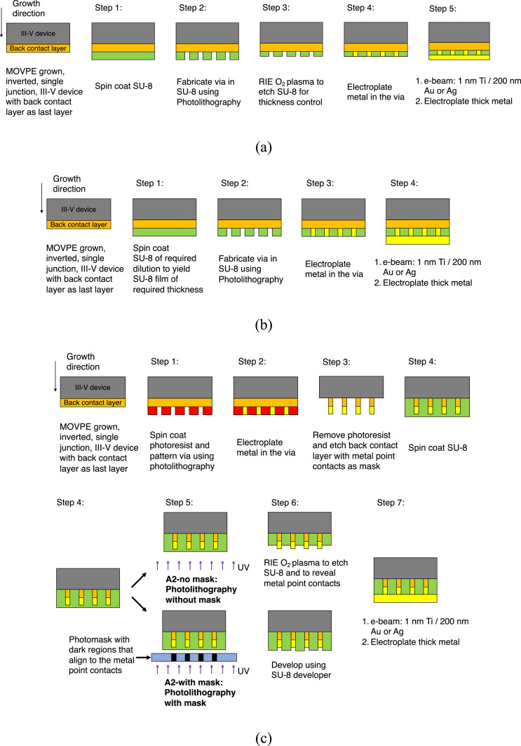
Fig. 3.
Schematic of PDBC fabrication process flow A, used primarily for SU-8 photoresist as the dielectric layer. Process A1 for SU-8 first process (a) A1-RIE – thickness control through RIE; (b) A1-spin – thickness control through SU-8 dilution; and (c) process A2 for metal point contact first process; for a structure in which the back contact layer is etched everywhere except at the point contacts; and shows the two different sub-processes A2-no mask and A2-with mask in steps 5, 6.

