

Abstract
Accurate coupling between optical modes at the interface between photonic chips and free space is required for the development of many on-chip devices. This control is critical in quantum technologies where large-diameter beams with designed mode profiles are required. Yet, these designs are often difficult to achieve at shorter wavelengths where fabrication limits the resolution of designed devices. In this work we demonstrate optimized outcoupling of free-space beams at 461 nm using a meta-grating approach that achieves a 16 dB improvement in the apodized outcoupling strength. We design and fabricate devices, demonstrating accurate reproduction of beams with widths greater than 100 μm.
1. Introduction
Integrated photonics are enabling new technologies for compact sensing [1], metrology [2], and quantum computing [3]. Many applications require light to be sent off chip—for example to interrogate isolated atomic media [4–7]—which benefit from the miniaturization and manufacturability of integrated photonics. Such designs require mode couplers capable of generating free-space beams with different wavelengths, polarizations, and beam geometries. As examples, beams with large numerical apertures or large beam waists may be required for projecting optical [8] and magneto-optical traps (MOTs) [9,10], respectively. Accurate beam control can be realized using on-chip outcouplers combined with planar metasurfaces to modify the beam phase profile and polarization state [11]. Such platforms enable the integration of beams of multiple colors, profiles, and polarizations for unparalleled control of optical fields within a compact three-dimensional space.
Proper design of photonic outcouplers is important for generating pristine free-space beams. Grating couplers, which operate based on Bragg scattering [12], are often needed when light is coupled into or out from the device surface. To optimally match modes at the interface, grating couplers may be apodized and subwavelength meta-grating (MG) elements incorporated to provide continuous control of the outcoupling strength [13]. While subwavelength MGs have found many applications at telecom wavelengths [14–17], their use in the visible is more restricted by the resolution of lithography and process variations [18]. In addition, material losses become a major concern at visible wavelengths, requiring the consideration of trade-offs between loss performance and fabricability [19].
In this work we utilize an apodized design of subwavelength MGs using a silicon nitride platform to create large mode diameter outcouplers at 461 nm. This wavelength is used for laser cooling strontium atoms in MOTs and atomic clocks [20,21]. By strictly accommodating the limits of electron-beam lithography in our MG design we fabricate outcouplers that accurately reproduce elliptical collimated Gaussian beams with waists larger than 100 μm. These beam profiles are strictly only achievable using a MG approach. Restricted by a minimum physical feature size of 30 nm, our MG design incorporates lines with effective widths down to 4.5 nm, providing a 16 dB improvement in the dynamic range of the outcoupling strength and smoother turn on of the beam profile compared to solid-line gratings. By establishing an equivalency between our MG and an effective solid-line design, we demonstrate an intuitive approach for calculating the required apodization using two-dimensional modeling. Our MG performance at 461 nm relies critically on the use of sub-diffractive elements, whose designed anisotropy could be exploited in future designs to enable added functionality and polarization control [22].
2. Meta-grating design and performance
The photonic outcoupler is based on a two-stage extreme mode converter that enables beam shaping along two independent axes [23], shown in Fig. 1(a). The first stage is an evanescent coupler (EVC) that converts a single waveguide mode into a collimated slab-mode beam. The EVC operates based on evanescent coupling, which is controlled by spatially varying the gap between the waveguide and the dielectric slab along the direction of propagation (see Fig. S1 in the Supplement 1). The second stage is the MG outcoupler that converts the slab-mode beam into a free space beam (side view in Fig. 1(b)). Beam shaping is achieved in both stages by spatially varying the coupling strength between successive optical modes according to:
| (1) |
where x is the propagation direction and Γ(x) is the spatially varying coupling strength required to achieve the beam power profile B(x), with unity total power [24]. Fig. 1(c–d) shows a Gaussian beam intensity profile with a 1/e2 radius w0 = 100 μm, and its corresponding Γ. This Gaussian profile has been truncated at 1.5w0 for realization within a finite-sized device.
Fig. 1.

Meta-grating outcoupler design (a) Extreme mode converter based on a two-stage design. The first stage is an EVC and the second is the MG outcoupler. Together the free-space beam can be shaped along two orthogonal directions (denoted red and yellow from each stage). (b) Side diagram of the apodized grating outcoupler, which shapes the beam profile and scatters collimated light into free space (yellow arrows). (c) An example Gaussian beam profile with a 100 μm beam waist. (d) Spatial variation of outcoupling strength required to generate the beam profile in panel c.
The example profile requires varying Γ over nearly three orders of magnitude, which can be difficult to achieve given fabrication limitations—specifically for the grating outcoupler if it is composed of a solid-line grating. We calculate Γ for both the EVC and the grating outcoupler as a function of design parameters using finite element method simulation. Our simulated device consists of a 150 nm thick silicon nitride (Si3N4) layer embedded in silicon dioxide (SiO2). For the EVC, we consider a uniform waveguide that is 100 nm wide and 150 nm thick and that couples in plane with a dielectric slab of the same thickness. With this geometry, the required range of Γ is achieved by varying the gap between the waveguide and the dielectric slab. Γ can be made arbitrarily weak by increasing the gap, while the strongest Γ requires a minimum gap of ≈ 200 nm, which is readily realizable using conventional lithography. In contrast, the grating outcoupler is more dependent on the minimum feature size. If we consider a single etch step design for the grating, then both the minimum and maximum Γ must be realized using the same etch depth. The strongest Γ is achieved at etch depths deeper than around 30 nm. If we chose this as our minimum depth, then the weakest Γ requires solid grating lines narrower than 5 nm, which is far below the resolution of electron-beam lithography based dry etch patterning.
To fabricate grating lines with weaker outcoupling strengths than can be realized with solid lines, we use the MG design shown in Fig. 2(a). The period of the MG, Λy, must be less than the wavelength of the slab mode to prevent in-plane scattering at normal incidence [13]. We consider a maximum Λy = 200 nm, which is smaller than the wavelength of the fundamental TE slab mode, which propagates with a mode index of ≈ 1.86. Considering that our minimal resolvable electron beam feature size is 30 nm, then the weakest MG line we can write has a filling fraction equal to that of a solid line with a width , where we define
| (2) |
and Wx and Wy are the widths of the MG element (minimally 30 nm) along the x and y directions, respectively.
Fig. 2.

Equivalence between meta- and solid-line gratings (a) A single MG line consisting of an array of subwavelength-sized etched elements. (b) A single line from a solid-line grating with the same width as the design in panel a. (c) The calculated outcoupling strength of the simulated MG (red), simulated solid-line grating (blue), and experimentally fabricated MGs as a function of . The experimental data includes designs with Λy = 200 nm (black data), Λy = 120 nm (green data), and with a solid grating design (orange data). Insets show optical images of the light scattered from several of the fabricated gratings, where the slab-mode light is incident from the left (denoted with a blue arrow). (d) The calculated change in outcoupling angle as a function of from the same data sets in panel c. In all experimental data, the error bars correspond to one standard deviation statistical uncertainly of the measurement.
Figs. 2(c–d) show that MGs perform nearly identically to their filling-fraction equivalent solid-line gratings. We consider a uniform MG with Wx = 50 nm, an etch depth of 37 nm, and Λx = 425 nm—the period of the grating along the direction of propagation. We vary the filling fraction by changing Wy and calculate Γ and the change in emission angle, Δθ = θ − θ0, as a function of the calculated (red data) and compare it to a design with the MG replaced by a solid line grating with line width (blue data). The MG is simulated in three dimensions with Floquet periodicity in the y-direction, while the solid-line grating is simulated in two dimensions. Both geometries assume no silicon substrate and an infinite oxide cladding. The two simulations model the same solid-line geometry (Fig. 2(b)), when Wy = Λy and thus , and where θ0 ≈ 2° and Γ0 ≈ 0.014 μm−1. Importantly, as is decreased, the two simulated gratings follow nearly identical trends, indicating an equivalency between the MG and its solid-line counterpart. As a result, two-dimensional simulations of solid-line gratings can be used to approximate the performance of MG designs and calculate grating apodization with fewer computational resources. Quantifying the accuracy of this approximation would be improved with more computational power than used presently. For example, when is less than 20 nm, the MG decay lengths, obtained by fitting the field intensity, are an order of magnitude longer than the simulation size. Above 20 nm, the two simulations agree to within 15 % for Γ and 3 % for θ. Simulating longer gratings would provide a more accurate comparison at small .
We observe similar trends in Fig. 2(c–d) with experimentally fabricated devices. These devices were fabricated as uniform MGs with nominally the same geometries as described for the MG simulations. MGs with several Λy as well as gratings with solid grating lines were fabricated with their decay profiles and outcoupling angles measured. The measured profiles for devices fabricated with Λy = 200 nm are provided in Fig. S2 in the Supplement 1. The experimental trends follow the simulations very closely. At smaller the experimentally measured Γ are slightly stronger than simulation, which is likely due to imperfect oxide filling of structures with smaller meta-elements.
3. Calculation of grating apodization
The results from Fig. 2 indicate that MG designs are well approximated by gratings with fill-fraction equivalent solid lines, which can be modeled in two dimensions. This approximation enables faster calculation of grating apodization, which we obtain from two finite element simulations. The first simulation performs a gradient descent optimization on a two-dimensional unit cell (inset in Fig. 3(a)) to find the period Λx that outcouples light at a design angle of θ = 30° for different and grating line depths. We solve a variant of the inverse problem and find the Λx that optimizes the power coupled into the slab mode from free space, assuming the cladding thickness extends indefinitely. The results from this simulation are shown in Fig. 3(a), illustrating that small variations around Λx ≈ 200 nm are required to maintain a uniform phase front along the grating. This is because as the higher index dielectric is removed when the grating element is etched deeper and wider, less phase is accumulated by the slab mode over the unit cell, and Λx must be slightly increased to match momentum with the free-space wave. The slight variations in Λx can be readily reproduced using electron-beam lithography and modified to adjust beam collimation off chip. The calculated data are fitted to a polynomial regression (black lines), which are used for interpolation of the apodization.
Fig. 3.
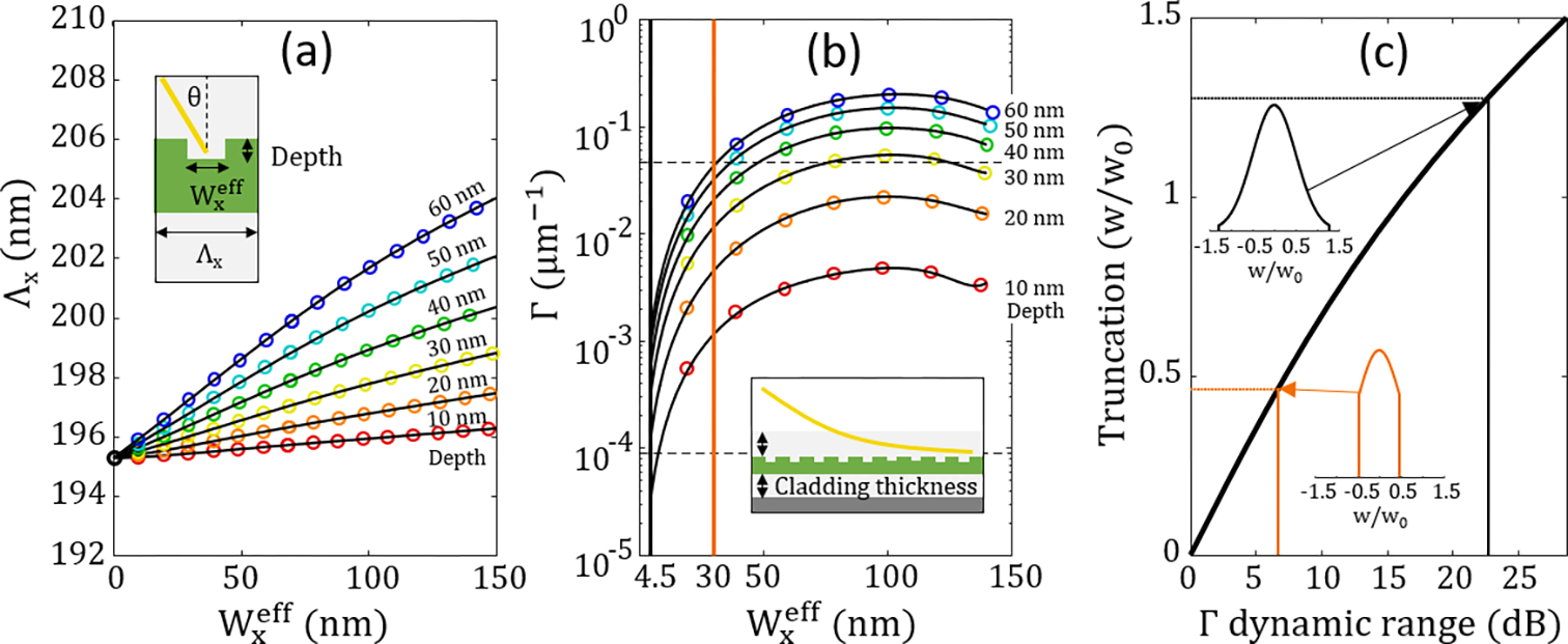
Parameterization of the grating design. (a) Calculated Λx with corresponding polynomial fits (black lines) for gratings that outcouple at θ = 30° into free space as a function of different grating depths and effective line widths. The inset shows the simulated unit-cell geometry that has periodic boundary conditions along the x-direction. (b) Calculated Γ with corresponding inverse polynomial fits (black lines) for uniform gratings with varied effective line widths and etch depths. The inset shows the two-dimensional geometry of the simulation, including top and bottom claddings and a silicon substrate. Horizontal dashed lines delineate the dynamic range of Γ from Fig. 1(d) and vertical lines at 30 nm (orange) and 4.5 nm (black) mark the minimum feature sizes for solid-line gratings and MG designs, respectively. (c) Required truncation of the Gaussian beam profile as a function of the Γ dynamic range. The orange and black lines and corresponding insets indicate the truncation for the solid-line grating and MG designs, respectively.
The second simulation models a uniform grating of many lines with period Λx, obtained from the first simulation. We calculate Γ, shown in Fig. 3(b), from the obtained decay profile (yellow curve in the inset), as the slab mode enters the grating from one side. Γ depends on the cladding thicknesses, so we simulate our experimental geometry with top and bottom cladding thicknesses of 0.5 μm and of 2.6 μm, respectively. The bottom cladding thickness can be chosen to provide constructive interference for maximal vertical outcoupling of power from the chip. The maximal simulated vertical outcoupling efficiency is ≈ 56 % and the minimal is ≈ 39 % based on simulations with varied cladding thicknesses. Simulation data are fitted to inverse polynomial regressions constructed such that Γ → 0 as . We mark the extrema from Fig. 1(d) along the vertical axis and clearly see that the etch depth must be at least 30 nm (yellow data) to reach the maximum required Γ, which occurs with nearly 50 % duty cycle gratings, i.e., when .
The dynamic range of Γ is largely independent of the grating depth, but it increases rapidly with the inclusion of smaller grating elements. Solid-line gratings, with limited to be greater than 30 nm, provide a dynamic range of (6.7 ± 0.2) dB, while the MG design, with limited to be greater than 4.5 nm, increases that range by (16.1 ± 0.1) dB for a total range of (22.8 ± 0.3) dB. All reported uncertainties are one standard deviation. Here the uncertainties are calculated from the variance in Γ for the different etch depths. The increase in dynamic range enables a smoother onset and improved reproduction of the desired Gaussian beam profile as seen in Fig. 3(c). For simplicity, we consider symmetric truncation, implying that some power will pass un-outcoupled through the grating. We show later how outcoupling can be maximized for a given truncated profile. If we assume that the depth of the grating can be freely chosen to match w0 then the dynamic range has a one-to-one correspondence with the truncation length (see Fig. S3 in the Supplement 1). A Gaussian profile truncated to ≈ 1.28 w0 can be realized using the MG dynamic range, in contrast with the ≈ 0.47 w0 truncation required by solid-line gratings. This difference is illustrated in the insets of Fig. 3(c). The profiles are better reproduced with the MG design (black profile), with the intensity range of control increasing from ≈ 35 % for solid gratings to ≈ 96 % for MGs.
A 30 nm etch depth provides the best coverage for a beam designed with a single etch step and w0 = 100 μm. The tradeoffs in apodizing at different etch depths are illustrated in Fig. 4, which plots the beam intensity and phase profiles (panels a-f) and corresponding apodized designs (panels g-l) for different etch depths. The apodized designs are obtained using the results from Fig. 3 by calculating how and Λx must change along the length of the grating to produce the desired beam profile according to eq (1). To calculate the optimal apodization, we truncate the Gaussian profiles for the given dynamic range of Γ to produce symmetric beam profiles.
Fig. 4.

Effect of etch depth on beam performance (a-f) Beam profiles (colored red to blue) and phase profiles (gray) obtained by two-dimensional simulation of solid-line gratings with apodizations calculated for different etch depths ranging from 10 nm to 60 nm, according to the colors introduced in Fig. 3. The y-axes are shared amongst panels a-f. (g-l) the apodization profiles used to generate the gratings simulated in (a-f). Each design begins with and is apodized according to a truncated Gaussian beam profile with a waist of 100 μm such that the outcoupled beam is symmetric. The y-axes are shared amongst panels g-l.
While ideal beam profiles have a smooth onset, Γ cannot be made arbitrarily weak since the minimum is fixed to 4.5 nm. The weakest Γ for each etch depth sets how steep the beam profile will be at its onset. Deeper etched gratings cause more abrupt onsets as seen in Fig. 4(e–f). There is a different tradeoff for shallower etched gratings—that less total power will be outcoupled from the slab mode over the same grating length. Weaker outcoupling allows some power to continue past the grating region. For example, the MGs with 10 nm and 20 nm etch depths only outcouple ≈ 42 % and ≈ 95 % of the available slab-mode power, respectively, while gratings with 30 nm or deeper etch depths can outcouple more than 99 % of the power. These percentages correspond to the amount of power leaving the slab mode, the efficiency of outcoupling vertically up versus down will depend on the exact cladding thickness and design of the grating substrate. Despite having truncated profiles, the deeper etched gratings can outcouple all the power by continuing the grating beyond where the beam is truncated. This leads to the exponential tails seen in Figs. 4(c–f) corresponding to the flat apodization in Figs. 4(i–l). While the beam profile is more accurately reproduced at the shallower etch depths, there is not enough grating length to outcouple all the power from the slab mode. As a result, the outcoupling strength is modulated with a shape similar to the beam profile itself, as seen in Fig. 4(g) compared to Fig. 4(a). In contrast, the design with the optimal etch depth around 30 nm has a nearly linear apodization (Fig. 4(i)). In all cases, the simulated apodizations produce beams with nearly flat phase profiles indicating that the calculated apodization follows well from the simulations in Fig. 3 and that the resulting beams should be nearly collimated.
4. Experimental meta-grating results
To maximize power outcoupling we choose an etch depth of nominally 37 nm for calculating our apodized design. We require two beam designs, one emitting nominally around 30° and the other around 8°. Both designs incorporate the same EVC, producing a nominal slab-mode beam waist of 100 μm. In the second stage, two different MGs are designed, producing numerically-simulated beam waists of ≈ 134 μm and ≈ 71 μm for the ≈ 30° and ≈ 8° beams respectively. Both gratings were designed using Λy = 120 nm. The previous analysis is then carried out according to eq (1) using these different beam waists for their corresponding outcoupling angles.
To fabricate our devices we use stoichiometric Si3N4 and two separate electron-beam lithography and reactive-ion etch steps. We use a through etch to fabricate the EVC and a nominal 37 nm partial etch to fabricate the MG. The device has a thermal oxide bottom cladding with a nominal thickness of 2.6 μm and is overgrown with a top oxide cladding using a low temperature oxide LPCVD process. The details of the fabrication process as well as SEM images of devices are provided in Fig. S4 and Fig. S5, respectively, in the Supplement 1. After depositing the cladding, the wafers are diced and the edges of the chip are then polished to expose waveguides terminated with a tapered edge coupler [25], which is used for coupling laser light on-chip with a cleaved fiber. Our measurement setup uses a 20× 0.75 NA objective mounted to a micrometer stage for imaging the grating emission onto a CCD camera and measuring the beam profile at different heights above the chip surface.
Fig. 5(a) shows an optical image of the beam emitted from the fabricated device of the 30° design. The blue arrow indicates the direction of the slab mode beam (not visible) coming from the EVC. Fig. 5(b) and (c) show the beam profile along the x and y-directions (with power integrated over the orthogonal direction) along with Gaussian fits. The beam has a fitted waist along x and y of wx = (128 ± 0.5) μm and wy = (81 ± 0.2) μm, respectively, where the uncertainty is obtained from Gaussian fitting parameter variance estimate. By measuring the beam at different heights off the chip (Fig. 5(d)) we obtain a measured value of θ = 30.1° ± 0.1°, where the uncertainty is obtained from fitting the beam trajectory to a straight line. As the beam propagates, the profile slightly focuses along the x and y directions as shown in Figs. 5(d, e). The focusing along x corresponds to an accumulation of phase along the length of the grating equivalent to approximately one λ over a length of 800 λ, which can be corrected by slightly modifying the results from the period simulation in Fig. 3(a). Figs. 5(f–j) show the corresponding measurements for the fabricated 8° device, which give wx = (89 ± 0.7) μm and wy = (80 ± 0.2) μm, θ = 8.69° ± 0.02°, and a focusing along the x direction equivalent to an excess accumulation of λ phase over a length of ≈ 725 λ. The performance of the EVC is functionally equivalent between the two devices, with wy ≈ 80 μm at z = 0 mm and a similar wy trend at different heights (Figs. 5(e) and (j)), but the 30° MG device matches the design parameters better than the 8° device. By incorporating feedback from experimentation to our apodization design, modifications can be made to further improve beam performance. Higher resolution images of the beam profiles at different heights shown in Figs. 5(d) and 5(i) are provided in Fig. S6 in the Supplement 1. While similarly good phase and angular performance can be achieved without utilizing a subwavelength MG design, it would have been impossible to successfully reproduce Gaussian beam profiles along the x-direction using solid grating lines. Attempts to do so yield beam profiles that were exponentially decaying, as seen in Fig. S7 in the Supplement 1.
Fig. 5.

Experimental results. (a) Optical image of the beam designed to emit at ≈ 30° from the MG. The slab mode beam is incident along the x direction from the left (denoted with a blue arrow). (b) Intensity profile of the beam along the length of the grating with a Gaussian fit (black line). The light yellow region corresponds to a one standard deviation measurement uncertainty of the beam intensity profile, obtained from different horizontal slices of the profile from panel a, while the dark yellow corresponds to the mean profile. (c) Intensity profile of the beam orthogonal to the grating with a Gaussian Fit (black line).The light red region corresponds to a one standard deviation measurement uncertainty of the beam intensity profile, obtained from different vertical slices of the profile from panel a, while the dark red corresponds to the mean profile. (d) Optical images of the beam taken at different heights above the chip. The separation between images is 2.5 mm. (e) Measured beam waist along x and y directions, yellow and red respectively, as a function of distance from the chip surface. (f-j) Data like that shown in panels (a-e), but for a beam designed with a narrower beam waist along the x direction that emits at ≈ 8° from the MG.
5. Conclusions
In this paper, we presented the experimental realization of grating outcouplers based on a subwavelength MG design that produces pristine beam profiles at blue visible wavelengths. We established the equivalency between MG designs and designs using solid grating lines, which enabled a speed up in the modeling of our fabricated structures by reducing the simulations from three to two dimensions. Through our two-dimensional analysis we explained the tradeoffs between choosing different etch depths for creating apodized gratings with large beam waists. Our design protocol is robust for calculating the apodizations of different beam shapes and beam angles and allowed us to push the limits of how large a beam can be designed at short wavelengths within the resolution of electron beam lithography. We showed that by using a MG design we could improve the dynamic range of the outcoupling strength by ≈ 16 dB and increase the range of control over the intensity profile by ≈ 60% compared to solid-line gratings. At 461 nm this improvement effectively differentiates between being able to accurately reproduce Gaussian beams and not.
The developed techniques and demonstrated devices extend the capabilities of on-chip photonic technologies, particularly for miniaturizing devices for quantum metrology and sensing. In the future, we plan to incorporate beams at different angles and with different colors on the same chip and integrate with meta-surfaces for controlling beam phase fronts and polarizations within a fully-planar structure. These devices will enable new on-chip technologies for interrogating atoms and other quantum media within small working volumes. By maintaining precise control of the beam properties, future designs may be able to incorporate anisotropic meta-grating elements to create beams with non-traditional polarizations and angular momenta for customizable design of integrated quantum devices.
Supplementary Material
Acknowledgements
The research was partially funded by the U.S. Defense Advanced Research Projects Agency (DARPA) under the Atomic-Photonic (A-PhI) program. The views and conclusions are those of the authors and should not be interpreted as representing the official policies of the funding agency. Dr. Chad Ropp and Dr. Alex Yulaev also acknowledge support under the Professional Research Experience Program (PREP), administered through the Department of Chemistry and Biochemistry, University of Maryland. Research performed in part at the National Institute of Standards and Technology Center for Nanoscale Science and Technology. We also would like to thank William McGehee, Kartik Srinivasan, and Jinghui Yang for helpful discussions.
Footnotes
Disclosures
The authors declare no conflicts of interest.
Supplemental document
See Supplement 1 for supporting content.
Data availability
Data underlying the results presented in this paper may be obtained from the authors upon reasonable request.
References
- 1.Passaro VMN, Tullio CD, Troia B, Notte ML, Giannoccaro G, and Leonardis FD, “Recent Advances in Integrated Photonic Sensors,” Sensors 12, 15558–15598 (2012). [DOI] [PMC free article] [PubMed] [Google Scholar]
- 2.Kitching J, Donley EA, Knappe S, Hummon M, Dellis AT, Sherman J, Srinivasan K, Aksyuk VA, Li Q, Westly D, Roxworthy B, and Lal A, “NIST on a Chip: Realizing SI units with microfabricated alkali vapour cells,” J. Phys.: Conf. Ser. 723, 012056 (2016). [Google Scholar]
- 3.Wang J, Sciarrino F, Laing A, and Thompson MG, “Integrated photonic quantum technologies,” Nature Photonics 14, 273–284 (2020). [Google Scholar]
- 4.Hummon MT, Kang S, Bopp DG, Li Q, Westly DA, Kim S, Fredrick C, Diddams SA, Srinivasan K, Aksyuk V, and Kitching JE, “Photonic chip for laser stabilization to an atomic vapor with 10−11 instability,” Optica, OPTICA 5, 443–449 (2018). [Google Scholar]
- 5.Mehta KK, Zhang C, Malinowski M, Nguyen T-L, Stadler M, and Home JP, “Integrated optical multi-ion quantum logic,” Nature 586, 533–537 (2020). [DOI] [PubMed] [Google Scholar]
- 6.Mehta KK, Bruzewicz CD, McConnell R, Ram RJ, Sage JM, and Chiaverini J, “Integrated optical addressing of an ion qubit,” Nature Nanotechnology 11, 1066–1070 (2016). [DOI] [PubMed] [Google Scholar]
- 7.Niffenegger RJ, Stuart J, Sorace-Agaskar C, Kharas D, Bramhavar S, Bruzewicz CD, Loh W, Maxson RT, McConnell R, Reens D, West GN, Sage JM, and Chiaverini J, “Integrated multi-wavelength control of an ion qubit,” Nature 586, 538–542 (2020). [DOI] [PubMed] [Google Scholar]
- 8.Sortais YRP, Marion H, Tuchendler C, Lance AM, Lamare M, Fournet P, Armellin C, Mercier R, Messin G, Browaeys A, and Grangier P, “Diffraction-limited optics for single-atom manipulation,” Phys. Rev. A 75, 013406 (2007). [Google Scholar]
- 9.Hoth GW, Donley EA, and Kitching J, “Atom number in magneto-optic traps with millimeter scale laser beams,” Opt. Lett., OL 38, 661–663 (2013). [DOI] [PubMed] [Google Scholar]
- 10.Chauhan N, Bose D, Puckett M, Moreira R, Nelson K, and Blumenthal DJ, “Photonic Integrated Si3N4 Ultra-Large-Area Grating Waveguide MOT Interface for 3D Atomic Clock Laser Cooling,” in 2019 Conference on Lasers and Electro-Optics (CLEO) (2019), pp. 1–2. [Google Scholar]
- 11.Yulaev A, Zhu W, Zhang C, Westly DA, Lezec HJ, Agrawal A, and Aksyuk V, “Metasurface-Integrated Photonic Platform for Versatile Free-Space Beam Projection with Polarization Control,” ACS Photonics 6, 2902–2909 (2019). [PMC free article] [PubMed] [Google Scholar]
- 12.Yariv A and Yeh P, Photonics: Optical Electronics in Modern Communications, 6th edition (Oxford University, 2006). [Google Scholar]
- 13.Halir R, Cheben P, Janz S, Xu D-X, Molina-Fernández Í, and Wangüemert-Pérez JG, “Waveguide grating coupler with subwavelength microstructures,” Opt. Lett., OL 34, 1408–1410 (2009). [DOI] [PubMed] [Google Scholar]
- 14.Chen X, Xu K, Cheng Z, Fung CKY, and Tsang HK, “Wideband subwavelength gratings for coupling between silicon-on-insulator waveguides and optical fibers,” Opt. Lett., OL 37, 3483–3485 (2012). [DOI] [PubMed] [Google Scholar]
- 15.Xu X, Subbaraman H, Covey J, Kwong D, Hosseini A, and Chen RT, “Complementary metal–oxide–semiconductor compatible high efficiency subwavelength grating couplers for silicon integrated photonics,” Appl. Phys. Lett. 101, 031109 (2012). [Google Scholar]
- 16.Cheng Z, Chen X, Wong CY, Xu K, and Tsang HK, “Apodized focusing subwavelength grating couplers for suspended membrane waveguides,” Appl. Phys. Lett. 101, 101104 (2012). [DOI] [PubMed] [Google Scholar]
- 17.Halir R, Bock PJ, Cheben P, Ortega-Moñux A, Alonso-Ramos C, Schmid JH, Lapointe J, Xu D-X, Wangüemert-Pérez JG, Molina-Fernández Í, and Janz S, “Waveguide sub-wavelength structures: a review of principles and applications,” Laser & Photonics Reviews 9, 25–49 (2015). [Google Scholar]
- 18.Song JH, Kongnyuy TD, Troia B, Saseendran SS, Soussan P, Jansen R, and Rottenberg X, “Grating devices on a silicon nitride technology platform for visible light applications,” OSA Continuum, OSAC 2, 1155–1165 (2019). [Google Scholar]
- 19.Blumenthal DJ, “Photonic integration for UV to IR applications,” APL Photonics 5, 020903 (2020). [Google Scholar]
- 20.Sorrentino F, Ferrari G, Poli N, Drullinger R, and Tino GM, “Laser cooling and trapping of atomic strontium for ultracold atoms physics, high-precision spectroscopy and quantum sensors,” Mod. Phys. Lett. B 20, 1287–1320 (2006). [Google Scholar]
- 21.Nicholson TL, Campbell SL, Hutson RB, Marti GE, Bloom BJ, McNally RL, Zhang W, Barrett MD, Safronova MS, Strouse GF, Tew WL, and Ye J, “Systematic evaluation of an atomic clock at 2 × 10 −18 total uncertainty,” Nature Communications 6, 6896 (2015). [DOI] [PMC free article] [PubMed] [Google Scholar]
- 22.Luque-González JM, Herrero-Bermello A, Ortega-Moñux A, Molina-Fernández Í, Velasco AV, Cheben P, Schmid JH, Wang S, and Halir R, “Tilted subwavelength gratings: controlling anisotropy in metamaterial nanophotonic waveguides,” Opt. Lett., OL 43, 4691–4694 (2018). [DOI] [PubMed] [Google Scholar]
- 23.Kim S, Westly DA, Roxworthy BJ, Li Q, Yulaev A, Srinivasan K, and Aksyuk VA, “Photonic waveguide to free-space Gaussian beam extreme mode converter,” Light: Science & Applications 7, 72 (2018). [DOI] [PMC free article] [PubMed] [Google Scholar]
- 24.Taillaert D, Bienstman P, and Baets R, “Compact efficient broadband grating coupler for silicon-on-insulator waveguides,” Opt. Lett., OL 29, 2749–2751 (2004). [DOI] [PubMed] [Google Scholar]
- 25.Marchetti R, Lacava C, Carroll L, Gradkowski K, and Minzioni P, “Coupling strategies for silicon photonics integrated chips [Invited],” Photon. Res., PRJ 7, 201–239 (2019). [Google Scholar]
Associated Data
This section collects any data citations, data availability statements, or supplementary materials included in this article.
Supplementary Materials
Data Availability Statement
Data underlying the results presented in this paper may be obtained from the authors upon reasonable request.