

ABSTRACT
Low-density films of single-walled carbon nanotubes (SWNTs) can be used as a semi-transparent top electrode for all-solution-processed film devices; however, their semiconductor characteristics vary depending on the experimental factors in their dispersion into solvents, and the sublayers are damaged as a result of solvent incompatibility. In this study, we report a solvent-compatible filter-transfer method for SWNT films stacked with silver nanowires (AgNWs), and evaluate the semiconductor characteristics through the p/n heterojunction with a Si wafer (SWNT/Si). AgNWs and SWNTs were successively filtered through their aqueous dispersion solutions using a membrane filter. The stacked semi-transparent films (AgNW/SWNT films with controlled densities) were successfully transferred onto glass plates and Si wafers. The transmittance at 550 nm revealed a window between 60% and 80% with a narrow sheet resistance range between 11 and 23 Ω □−1. The power conversion efficiency (PCE) of SWNT/Si was improved to 11.2% in a junction area of 0.031 cm2 through the use of spin-coated Nafion resins; however, the accumulated resistance of SWNTs drastically reduced the PCE to 2% as the area increased to ≥0.5 cm2. AgNWs maintained the PCE within a range of 10.7% to 8.6% for an area ranging from 0.031 cm2 to 1.13 cm2. All of the photovoltaic parameters were dependent on the junction areas, suggesting that AgNWs function as an effective current-collector layer on the semiconductor layer of SWNTs without direct contact of AgNWs with the Si surface. In addition, we report a solvent-compatible experiment for transferring AgNW/SWNT films onto a solvent-sensitive perovskite material (CH3NH3PbI3).
KEYWORDS: Silver nanowire, carbon nanotube, solar cell, filter-transfer method, semi-transparent electrode
GRAPHICAL ABSTRACT

1. Introduction
Following the global trend of saving energy and resources, low-temperature solution processes have attracted the attention of researchers attempting to fabricate state-of-the-art film devices. Therefore, research is being conducted on technologies that consume less energy and material. However, vacuum-evaporated metals are currently employed for top electrodes for most film devices. Despite the increasing interest in developing all-solution-processed film devices, there are obstacles owing to the dispersion solutions of conductive nanomaterials, such as Ag nanoparticles (AgNPs) [1], Ag nanowires (AgNWs) [2–7], and carbon nanotubes (CNTs) [8], namely, (i) excess surfactants and/or surface-capping molecules surrounding nanomaterials prevent mutual electrical contact in solution-processed electrodes [9], and (ii) dispersion solvents and additives damage solvent-sensitive sublayers [5,7].
Transparent electrodes have been explored with the trade-off between optical transparency and electrical conductivity for creating energy and electronic devices, as exemplified by solar cells [10,11] and light emitting diode devices [12]. Indium – tin oxide and fluorine-doped tin oxide are indispensable to produce transparent bottom electrodes; however, low-temperature solution-processable technologies for such high-performance metal oxides hamper their application as transparent top electrodes [13,14]. Cost-effective metal nanowires have been employed [2–7,15]. Among them, dispersion solutions of AgNWs are homogeneously spread on various substrates by simple solution processes to obtain films for use as the bottom electrode [2,13–15]. The low-density AgNW films adhered to substrates are high-performance semi-transparent electrodes exhibiting visible-light transmittance and sheet resistance comparable to those of indium – tin oxide and fluorine-doped tin oxide [2,15], while the achieved conductivity originates from an inherently different mechanism. As AgNW films attain lower densities to increase the transmittance, open spaces between the wires are inevitably increased, as seen in a field-emission scanning electron microscope (FE-SEM) image (Figure 1(a)). Although low sheet resistance is macroscopically measurable, the increased interwire open spaces (i.e., non-conductive voids) are a microscopic shortcoming, limiting the application of AgNWs to certain types of devices. Semi-transparent mixed films of AgNWs and CNTs have been prepared to compensate for this shortcoming [16–20].
Figure 1.

FE-SEM images of AgNW and SWNT films on glass plates. (a) AgNW film (AgNW/glass) with a density of 6.7 μg cm−2. (b) SWNT film (SWNT/glass) with a density of 1.7 μg cm−2. (c) SWNT film stacked with AgNWs (AgNW/SWNT/glass) with the same densities. SWNT films are composed of bundled structures.
In 2010, Rinzler et al. reported that a Si heterojunction structure, SWNT/Si, was formed by adopting a solution-processed semi-transparent film of single-walled CNTs (SWNTs) [21]. SWNT/Si solar cells have been fabricated using various solution-processed methods, and their performance has been greatly improved to achieve high power conversion efficiencies (PCEs) [21–35]. We focus on semi-transparent SWNT film stacked with AgNWs, referred to as AgNW/SWNT film, reported by Taylor et al. in 2014 [22]. In the Si heterojunction solar cell, AgNW/SWNT/Si, the PCE reached 10.8% in a junction area of 0.49 cm2, where a dispersion solution of AgNWs was spin-coated on a p-type semiconductor layer of SWNTs to prepare a current-collector electrode. Top CNTs have been utilized as not only current-collector electrodes but also hole transfer layers (HTLs), and HTL-free perovskite (PVK) solar cells have been demonstrated recently [36–41]. In HTL-free solar cells showing bifacial transparency [42], there is a trade-off between visible-light transmittance and sheet resistance of SWNT films. To address this trade-off, it remains a challenge to place AgNW/SWNT films onto solvent-sensitive PVK materials without damage [5–7,15]. Since the usual aqueous dispersion solutions of SWNTs and AgNWs are utilized to fabricate all-solution-processed devices, it is necessary to develop a solvent-compatible technology to overcome the above-mentioned obstacle ii (solvent incompatibility).
In this study, AgNWs are stacked with a semi-transparent film of SWNTs that have small diameters of 1–3 nm (Figure 1(b,c)). AgNWs have large diameters, from several tens to hundreds of nm, and long lengths, from several tens of μm to 100 μm [15,43]. SWNTs appropriately match low-density AgNWs because the diameters of AgNWs are much larger than the bundle widths of SWNTs. However, the varied semiconductor characteristics of SWNT films with current-collecting abilities are still hotly debated because they undergo complex changes due to experimental factors, such as the crystallinity, bundle lengths, and widths of SWNTs, alignment of SWNTs, various surfactants to disperse SWNTs, and p-type chemical doping [23,24,44]. Therefore, we must first evaluate the characteristics of SWNT films used in this study, where SWNT/Si solar cells are employed as a suitable model for reliable evaluation through comparison with information on their characteristics obtained from previous reports [21–47]. Furthermore, since SWNTs act as an independent HTL by filling the open spaces of AgNWs (Figure 1(c)), it is necessary to develop a method to overcome obstacle iii – current-collector AgNWs penetrating the loose HTL through the inter-tube spaces of SWNTs (Figure 2(a))—because direct contact between AgNWs and the photoactive material significantly degrades the photovoltaic performance. Note that AgNPs and vacuum-evaporated metals penetrate the loose middle layer (Figure 2(b)) [35].
Figure 2.

Schematic drawing of top electrodes composed of nanomaterials with different morphologies, (a) AgNWs and (b) AgNPs, for all-solution-processed film devices. A specific solar cell structure is considered, in which a semi-transparent SWNT film is placed as a middle semiconductor layer on a photoactive material such as silicon and a solvent-sensitive perovskite. If the AgNPs make contact with the photoactive material by penetrating the loose structure of SWNTs, the performance of the film device will be significantly degraded. In this study, AgNWs can avoid such penetration by a filter-transfer method. note that vacuum-evaporated metals similarly penetrate the loose structure of SWNTs [35].
In this study, we present a solution-processed method for preparing semi-transparent AgNW/SWNT films with systematically controlled densities. Specifically, by overcoming obstacles ii and iii – solvent incompatibility and penetration, respectively – we achieve significant progress from previously reported filter-transferred semi-transparent SWNT films [48]. AgNWs and SWNTs are successively filtrated on a polytetrafluoroethylene (PTFE) membrane filter through dispersion solutions (Figure 3). The stacked AgNW/SWNT film adheres to glass plates with the assistance of the wettability of the membrane. After the evaporation of the wet solvents, a semi-transparent AgNW/SWNT film spontaneously transfers onto the glass plate apart from the membrane (Pathway 2 in Figure 3, and Video S1). The relationship between the sheet resistance and visible-light transmittance of the AgNW/SWNT films is systematically investigated by varying the film densities. AgNW/SWNT films are similarly transferred onto Si wafers to form AgNW/SWNT/Si solar cells, and the photovoltaic performance is compared with and without AgNWs. When SWNTs are doped with Nafion, AgNWs maintain the high PCEs even when the junction areas are increased to over 1 cm2. The photovoltaic parameter values systematically depend on the junction areas. Through a solvent-displacement process, the AgNW/SWNT film is successfully transferred to a solvent-sensitive PVK material (CH3NH3PbI3) without damage.
Figure 3.
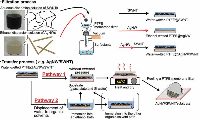
Schematic diagram of a solution-processed filter method for transferring SWNT, AgNW, and their stacked AgNW/SWNT films onto various substrates, such as glass plates and etched Si wafers [48]. surfactants and additives dissolved in dispersion solutions of SWNTs and AgNWs are washed away with solvents through a PTFE membrane filter. In a typical case of pathway 1, a water-wetted PTFE@AgNW/SWNT adheres to various substrates with the assistance of the wettability and flexibility of the membrane without any external pressure. In pathway 2, a water-wetted PTFE@AgNW/SWNT is immersed into an ethanol bath to displace the wet solvent of water. The water can also be displaced by washing with ethanol in a filtration process. If needed, the wet solvent, ethanol, can be further displaced with other organic solvents based on solvent-compatibility experiments with the target materials, such as a solvent-sensitive perovskite. The AgNW/SWNT films spontaneously transfer onto the substrates after the low-temperature evaporation of the wetted solvents, such as water, ethanol, and toluene, followed by peeling of the PTFE membrane filters. In this study, ethanol was employed as a common wetted solvent to transfer SWNT, AgNW, and AgNW/SWNT films onto glass plates and surface-etched Si wafers (Video S1).
2. Experimental details
2.1. Materials and chemicals
SWNTs (eDIPS EC1.5-P, >99%, 1–3 nm diameters) were purchased from Meijo Nano Carbon. Sodium dodecylbenzenesulfonate (SDBS) (>95%) and polyvinylpyrrolidone (PVP; K90) were obtained from Tokyo Chemical Industry. Guaranteed-grade AgNO3 and CuCl2∙2 H2O were used as supplied by Kanto Chemical and Nacalai Tesque, respectively. Guaranteed-grade ethylene glycol (EG), ethanol, and toluene were supplied by Kanto Chemical. For the filter-transfer method, hydrophobic PTFE membrane filters (POREFLON HP-010-30, 100-nm pore size) were purchased from Sumitomo Electric. Commercially available slide glasses (Matsunami Glass S1127) were divided into glass plates (2.5 × 2.5 cm2), and a sonication bath was used to wash the plates once with a cleaning liquid (AS ONE SDNU-N4), twice with water, once with acetone, and once with isopropanol. Si wafers (200-nm thick; SiO2, 1–20 Ω cm) were purchased from Optostar. Polyethylene terephthalate (PET) films (Toray Lumirro #100-T60) were washed with the cleaning liquid, twice with water, and once with isopropanol in a sonication bath prior to use. For p-type doping of SWNTs, a Nafion solution (5 wt% in a mixture of lower aliphatic alcohols and water [45%]) was obtained from Sigma Aldrich.
2.2. Preparation of dispersion solutions of SWNTs
An aqueous dispersion solution of SWNTs was prepared according to a previous report [48]. A small portion of SWNTs (1.16 mg) was vigorously stirred with an aqueous solution (20 mL) of 0.50 wt% SDBS using a homogenizer (HSIANGTAI HG-200) with a cutting head generator (K-7S) at 9000 rpm for 30 min in a cooled water bath at 5°C. The homogenized SWNT suspension was sonicated in a cooled water bath at 5°C under pulse-irradiation conditions of 0.4 s per second for 3 min using a low power of 5 W at 19.9 Hz by a probe-type sonicator (Branson Sonifier 250). After centrifugation at a controlled gravity of 2600 g for 20 min at 5°C, a homogeneously dispersed SWNT supernatant (18 mL) was obtained with a conversion yield of 60%. An aqueous solution (18 mL) of 0.50 wt% SDBS was added to the residual portion, including the SWNT precipitate. The mixture was homogenized, sonicated, and centrifuged using the same procedures. The second homogeneously dispersed SWNT supernatant (18 mL) was added to the first one (18 mL), and the dispersed SWNT aqueous dispersion solution (36 mL) was obtained with a total conversion yield of 90% or more. In a typical case, the obtained SWNT aqueous dispersion solution was used with a concentration of 25 μg mL−1 as a stock solution, where the concentration was determined based on a calibration curve method using photo-absorption intensities at 550 nm [48].
2.3. Preparation of dispersion solutions of AgNWs
AgNWs were prepared in accordance with the literature [43]. An EG solution (10 mL) of AgNO3 (0.170 g, 1.00 mmol), an EG solution (10 mL) of PVP (0.170 g), and an aqueous solution (0.15 mol L−1, 20 μL) of CuCl2 were added to a Teflon reaction vessel. After setting the vessel in a pressure-resistant container, the mixture solution was heated at 160°C for 3 h. The prepared dispersion solution containing AgNWs was used as a stock solution without purification because excess PVP molecules, unreacted Ag+ ions, and Ag nanoparticles were removed by a filtration process through a PTFE membrane filter to prepare AgNW films.
To determine the concentration of AgNWs in the stock solution, a solvent mixture (37 mL) of water and ethanol (1:1 v/v) was added to a small portion of the stock solution (3.0 mL). The AgNWs were selectively centrifuged under a controlled gravity of 6300 g for 10 min, and the supernatant containing unreacted Ag+ ions and Ag nanoparticles was removed. The precipitated AgNWs were further washed with water. After drying under reduced pressure, the weight of the purified AgNWs was estimated by thermogravimetric analysis (Shimadzu TGA-50) after the thermal removal of surface-capping PVP and EG molecules adhering to AgNWs. In a typical case, the concentration of the stock solution was estimated to be 4.2 mg cm−2, where the conversion yield from AgNO3 to AgNWs was 78%.
2.4. Filter-transfer of SWNT films onto glass plates
Semi-transparent SWNT films were transferred in accordance with a previous report (Pathway 2 in Figure 3) [48]. Aqueous dispersion solutions of SWNTs of various concentrations were prepared by adding water to the stock solution. The diluted aqueous dispersion solution was vacuum-filtered through a hydrophobic PTFE membrane filter, where the hydrophobic membrane pores were filled with ethanol before filtration. The filtrated SWNTs were carefully washed with water three times to remove the SDBS surfactant molecules. The SWNT film adhering to the water-wetted PTFE membrane (PTFE@SWNT) was immersed in an ethanol bath. The ethanol-wetted PTFE@SWNT adhered to a glass plate with the assistance of the solvent wettability and flexibility of the wetted membrane without any external pressure. The SWNT film spontaneously transferred onto the glass plate by peeling off the PTFE membrane after evaporation of ethanol by heating at 70°C.
2.5. Filter-transfer of AgNW films onto glass plates
AgNW dispersion solutions of various concentrations were prepared by adding ethanol to the stock solution. Semi-transparent AgNW films were transferred onto glass plates using the diluted dispersion solutions by procedures similar to those of SWNTs, where the filtrated AgNWs were carefully washed three times through a PTFE filter with ethanol to remove excess PVP molecules, unreacted Ag+ ions, and Ag nanoparticles.
2.6. Filter-transfer of AgNW/SWNT films onto glass plates
A diluted AgNW dispersion solution with ethanol was similarly filtered on a PTFE membrane filter and washed with ethanol three times, and a diluted SWNT aqueous dispersion solution was further filtered on the AgNW filtrated through the PTFE membrane (PTFE@AgNW). After washing three times with water, the as-stacked water-wetted PTFE@AgNW/SWNT was immersed in an ethanol bath. By procedures similar to those of SWNTs, semi-transparent AgNW/SWNT films were transferred onto glass plates to prepare AgNW/SWNT/glass after heating at 70°C (Pathway 2 in Figure 3, and Video S1). The wet ethanol solvent was further displaced by toluene by immersing in a toluene bath, where toluene was used after dehydration with molecular sieves 4A. After evaporation of toluene at 70°C, the stacked AgNW/SWNT semi-transparent film was similarly transferred onto the glass plate.
In a feasibility experiment to construct solution-processed semi-transparent electrodes for flexible film devices, the stacked AgNW/SWNT semi-transparent film was similarly transferred onto a PET film from an ethanol-wetted PTFE@AgNW/SWNT.
2.7. SWNT/Si and AgNW/SWNT/Si heterojunction solar cells
A Si wafer (1.5 × 1.5 cm2) with a 200-nm thick SiO2 layer was masked using polyvinyl chloride (PVC) tape except for round photoactive areas from 0.031 to 1.13 cm2. A diluted aqueous HF solution (5%) was dropped on the Si wafer to remove the SiO2 layer. After removing the PVC tape, semi-transparent SWNT and AgNW/SWNT films were transferred onto the surface-etched Si wafers by similar procedures (Pathway 2 in Figure 3). To improve the photovoltaic performance, a diluted Nafion resin solution with isopropanol (2.0 wt%, 100 µL) was coated on the formed SWNT/Si or AgNW/SWNT/Si heterojunctions by spin-coating at 1000 rpm for 5 s and then at 2000 rpm for 60 s, and the Nafion-coated heterojunctions were annealed at 140°C for 10 min [28]. Vacuum-deposited Au on a black PVC plate was contacted as the top electrode. A low-melting-point alloy of In:Ga = 1:1 (mol/mol) was employed as the bottom electrode.
2.8. Filter-transfer of an AgNW/SWNT film onto a PVK material
According to a previous report [48], a PVK (CH3NH3PbI3) layer was directly prepared on a glass plate. Toluene-wetted PTFE@AgNW/SWNT was placed on the PVK crystal layer without any external pressure, where the densities of AgNWs and SWNTs were 6.7 and 1.7 μg cm−2, respectively. After evaporation of toluene at 70°C, a stacked semi-transparent AgNW/SWNT film spontaneously transferred onto the PVK layer.
2.9. Characterization
A four-point probe technique (Kyowariken K-705RS) was used to measure the sheet resistance of semi-transparent films composed of SWNTs and AgNWs. The transmittance and relative reflection spectra were recorded on an ultraviolet – visible–near-infrared (UV – Vis–Near-IR) spectrophotometer (Shimadzu UV-2600), where the reflection spectra were obtained using a specular reflectance attachment (5° angle of incidence) and an Al mirror reference. Top-view field-emission scanning electron microscope (FE-SEM) images of the films were observed using a JEOL JSM-7600F. The distribution histogram of AgNW lengths was based on laser microscope images (Lasertec Optelics Hybrid L3). For low-density AgNW films, measuring the sheet resistance was difficult using the four-point probe technique; therefore, the sheet resistance was estimated by supporting Ag electrodes with a measurement area of 6 (width) × 5 (length) mm by using a digital multi-meter (Sanwa, PC7000). In the feasibility experiment for flexible film devices, the resistance values of an AgNW/SWNT film on a PET substrate were measured with various bent angles by using a digital multi-meter (Sanwa, PC7000). The structure of PVK was investigated by X-ray diffraction (XRD) patterns (Rigaku MiniFlex II, Cu Kα1 radiation). J–V curves were recorded on a source meter (Keithley 2400) by using a solar simulator (Peccell PEC-L01) under irradiation of pseudo-sunlight (AM1.5, 100 mW cm−2), where the irradiation intensity was calibrated by a Si photodiode (BS-500BK SN/179). External quantum efficiency (EQE) spectra were recorded on an action spectrometer (Peccell PEC-S20 with a Xe lamp [150 W]) by a Si photodiode reference (S1337–1010 BQ).
3. Results and discussion
3.1. Filter-transfer of SWNT films
As previously reported [48], long bundled SWNTs up to 19 µm were stably dispersed with high conversion yields of 90%. The controlled-concentration SWNT aqueous dispersion solutions passed through a hydrophobic PTFE membrane filter (Figure 3). A water-wetted SWNT film filtrated on a PTFE membrane, PTFE@SWNT, adhered to various substrates with the assistance of the wettability and flexibility of the PTFE membrane without any external pressure. After evaporation of water at 90°C, the SWNT film spontaneously transferred onto the substrates by peeling off the PTFE membrane (Pathway 1 in Figure 3). In this study, the wet solvent, water, was displaced with ethanol to systematically compare the relationship between the sheet resistance and the visible-light transmittance of similarly transferred AgNW films (AgNW/glass) and AgNW-stacked SWNT films on glass plates (AgNW/SWNT/glass), where the ethanol-wetted PTFE@AgNW and PTFE@AgNW/SWNT were heated at 70°C on the substrates for the evaporation of ethanol (Pathway 2 in Figure 3).
The relationship between the sheet resistance and transmittance for different loaded SWNT densities is presented in Figure 4 and Table S1, and the transmittance spectra are presented in Figure S1 [48–51]. For a typical density of 1.7 μg cm−2, corresponding to transmittance at 550 nm of 80%, the pristine SWNT film exhibited a sheet resistance of 103 Ω □−1. The SWNT films were homogeneously loaded onto glass plates by the filter-transfer method, but they were composed of bundled nanotubes, as illustrated in the FE-SEM images (Figure 1b and S2a). Based on the images, the bundled SWNTs were distributed from 4 to 50 nm in width, and the mean width was 15.2 nm on a glass plate (Figure S2b).
Figure 4.

Relationship between sheet resistance and transmittance at 550 nm for SWNT (●), AgNW ( ), and stacked AgNW/SWNT (
 and
and  ) films transferred onto glass plates. The AgNW/SWNT films were prepared by changing the loading densities of SWNTs from 0.86 to 2.6 μg cm−2 on AgNWs of two different constant densities, 6.7 (
 ) and 9.3 μg cm−2 (
 ) (Table S1). For the SWNT and AgNW/SWNT films, the error bars are based on five transmittance and nine sheet-resistance measurement points of each sample using the four-point probe technique.
3.2. Filter-transfer of AgNW films
In the synthesis of AgNWs, an excess amount of PVP was employed as a surface-capping polymer [43]. Excess PVP molecules contribute to the stable and homogeneous dispersion of AgNWs (Figure S3a); however, it is necessary to purify the AgNWs by removing the excess PVP molecules, Ag nanoparticles, and unreacted AgNO3 because, as an insulator, PVP greatly contaminates AgNW films [9]. A possible purification method is the centrifugation of AgNWs and the redispersion of the centrifuged AgNWs into solvents by sonication. However, we observed that centrifugation often resulted in flocculated AgNWs (Figure S3b). The flocculation deteriorated the redispersion states of AgNWs, and the sonication caused shorter lengths of AgNWs. Therefore, we used the initial homogeneous dispersion solution as a stock solution of AgNWs without further purification (Figure S3a) because the excess PVP molecules, Ag nanoparticles, and unreacted AgNO3 can be simply removed by passing them through a PTFE membrane filter for preparing the AgNW film (Figure 3). The purification-free process is an advantage of the filter-transfer method.
In a typical synthesis, the concentration of AgNWs dispersed in the stock solution was determined to be 4.2 mg mL −1 with a conversion yield of 78% by thermogravimetric analysis after the thermal removal of surface-capping PVP molecules adhering to the centrifuged AgNWs (Figure S4). AgNWs were distributed from 60 to 200 nm in width, and the mean diameter was 116 nm based on FE-SEM images (Figure S5a). AgNW lengths ranged from 10 to 155 μm based on laser microscope images (Figure S5b). AgNWs resembled straight rods in the submicrometer magnification range (Figure S5a) but could bend in the tens-of-micrometers range (Figure S5b).
In the filter-transfer process of AgNW films, diluted dispersion solutions of AgNWs with ethanol were used (Figure 3), and the film attached to the PTFE membrane filter was washed with ethanol to remove the excess PVP molecules [9], Ag nanoparticles, and unreacted AgNO3. The selection of washing solvents is key. When water was employed as a washing solvent, AgNWs were immediately suspended in water apart from the PTFE surface (Figure S6). To overcome obstacle iii (penetration) (Figure 2(a)), the formation process of AgNWs overlaid with homogeneous SWNT films on the membrane was unsuccessful due to the suspension behavior of AgNWs. The sheet resistance – transmittance relationship, depending on the loading densities of AgNW films transferred onto glass plates from the ethanol-wetted PTFE@AgNW, is summarized in Figure 4 and Table S1, and the transmittance spectra are presented in Figure S7. The electrical conductivity of AgNW films varied within a narrow sheet resistance range between 12 and 29 Ω □−1, corresponding to transmittance at 550 nm of 77% and 88%, respectively. The sheet resistance abruptly decreased when the transmittance exceeded 90% in low-density AgNW films, suggesting that the number of contact points of mutual AgNWs was decreased. In the case of transmittance at 550 nm of 92% and sheet resistance of 125 Ω □−1 (Figure 4), AgNWs were randomly distributed with a low-density (6.7 μg cm−2) on the glass plate, as illustrated in the low-magnification FE-SEM image (Figure S8), where the large error bar indicates the existence of many contact defects of AgNWs in their low-density film.
3.3. Filter-transfer of AgNW/SWNT films
The first layer of AgNWs was homogeneously overlaid with SWNTs on a PTFE membrane filter by a two-step filtration process (Figure 3). After washing with water, the stacked film on the PTFE membrane (water-wetted PTFE@AgNW/SWNT) was immersed in an ethanol bath to remove water, and the stacked AgNW/SWNT film was successfully transferred onto a glass plate from the ethanol-wetted PTFE@AgNW/SWNT (Pathway 2 in Figure 3, and Video S1). In the filter-transfer process, the SWNT side was directly attached to the glass surface to form a stacked structure on the glass plate (AgNW/SWNT/glass) (Figure 1(c)). On the basis of the performance of the individually prepared films of SWNTs and AgNWs depending on their loading densities, the sheet resistance – transmittance relationship of AgNW/SWNT/glass was systematically investigated, as summarized in Figure 4 and Table S1. In this study, we aimed to evaluate the current-collecting and semiconducting abilities of AgNWs and SWNTs by employing heterojunction SWNT/Si solar cells; therefore, the SWNT densities varied between 0.86 and 2.6 μg cm−2, corresponding to sheet resistance (transmittance at 550) between 201 (90%) and 58 (70%) Ω □−1, where low-density AgNWs of 6.7 and 9.3 μg cm−2 were used to fabricate stacked AgNW/SWNT films to obtain high optical transparency.
For AgNW/SWNT/glass, we found that the sheet resistance and transmittance largely depended on the density of AgNWs and SWNTs, respectively. A transmittance window between 60% and 80% was observed with a narrow sheet resistance range between 11 and 23 Ω □−1 (Figure 4 and Table S1), suggesting that the sheet resistance of AgNW/SWNT/glass strongly depends on the much higher electrical conductivity of AgNWs than that of SWNTs. The stacked AgNWs reduced the transmittance at 550 nm through the SWNT films by 10% or more (Table S1). In such low-density AgNW/glass, measuring sheet resistance was difficult using the usual four-point probe technique because AgNWs made no contact with the narrow probe tip; therefore, the sheet resistance was estimated using supporting Ag electrodes by a two-probe technique (Figure S9) [17]. In the stacked AgNW/SWNT films, measuring the sheet resistance was possible using the four-point probe technique. This indicates that macroscale electrical conductivity via the AgNW network is assisted by the local percolation networks of SWNTs sufficiently filling the interwire open spaces of AgNWs (Figure 1(c)). Thus, the conduction paths of the stacked AgNW/SWNT film are reinforced by the contact networks between AgNWs and SWNTs, suggesting that obstacle i owing to surfactants and/or surface-capping molecules can be overcome by a filter-transfer method that includes a careful process of washing excess surfactants and surface-capping molecules.
The feasibility to construct solution-processed semi-transparent electrodes for flexible film devices was investigated in a preliminary experiment. The stacked AgNW/SWNT film was successfully transferred onto a PET film. The electrical conductivity of the AgNW/SWNT film was investigated at different bending angles, as shown in Figure S10. The bent-to-unbent resistance ratios were slightly decreased in the steep angles. It is suggested that the mutual network of AgNWs and SWNTs forms a sheet of semi-transparent conductive film on the flexible substrate and the film can be applied as top electrodes on flexible devices.
3.4. Nafion doping
To enhance the p-type semiconductor characteristics of SWNTs, simple hole doping was possible by intercalation into SWNT bundles using inexpensive Brønsted acid molecules, such as HCl, HNO3, and H2SO4. It was revealed that H2SO4 doping resulted in a lower EF level of SWNTs than that with HNO3 or HCl doping [52]. Although the increased stored potential due to the lower EF can contribute to obtaining high Voc in Si heterojunction solar cells (SWNT/Si) [21], there is a trade-off; namely, volatility is helpful for removing excess acid molecules from SWNTs by heating, but doping is not stable because of the easy desorption of the acid molecules from SWNTs. Alternatively, Nafion resins are a typical non-volatile polymer bearing strong acid moieties of SO3H. In accordance with previous reports [28,45], we directly spin-coated a Nafion solution onto a pristine SWNT film transferred onto a glass plate (SWNT/glass) for p-type doping. The sheet resistance was reduced to 78 from 103 Ω □−1 for transmittance at 550 nm of 80%. A similar Nafion-coating process for a stacked film of AgNW/SWNT/glass reduced the sheet resistance to 13 from 20 Ω □−1, where the densities of AgNWs and SWNTs were 6.7 and 1.7 μg cm−2, respectively. Consequently, Nafion resins apparently did not provide a contact barrier between AgNWs and SWNTs as an insulator by the post-doping process. The electron-withdrawing effect and/or physically and chemically adsorbed oxygen induced by the SO3H acid moieties led to increased hole doping. The improved carrier-flow via tube – tube contact improved the electrical conductivity of SWNT films in SWNT/glass and AgNW/SWNT/glass [53]. Nafion doping also lowered the EF levels of SWNTs because the open-circuit voltage (Voc) was increased in Si heterojunction solar cells, as described in the following subsection (Tables S2 and S3).
3.5. SWNT/Si and AgNW/SWNT/Si heterojunction solar cells
SWNT films were transferred onto surface-etched Si wafers with a small junction area of 0.031 cm2 from ethanol-wetted PTFE@SWNT (Pathway 2 in Figure 3). According to previous reports [25,47], the photovoltaic performance of the formed heterojunction solar cell structure (SWNT/Si) was investigated in relation to three different values of transmittance at 550 nm, 70%, 80%, and 90% (Table S1), as summarized in Figure 5 and Table S2. For 70% and 80% transmittance, the averaged PCEs exhibited comparable values of 4.8% and 4.5%, respectively. The average Voc values of 0.41 and 0.42 V were also comparable. Because of the increased transparency from 70% to 80%, the averaged short-circuit current density (Jsc) improved slightly from 22.5 to 23.9 mA cm−2. As the sheet resistance (transmittance at 550 nm) of the SWNT films increased from 58 (70%) to 103 (80%) Ω □−1, the average fill factor (FF) decreased from 52 to 44%. The series resistance (Rs) of SWNT/Si was estimated from the J–V curves (Table S2). In typical cases, the Rs values were estimated to be 4.9 and 5.2 Ω cm2 for the 70% and 80% transmittance, respectively, suggesting that the increased sheet resistance of SWNT films was correlated with the degraded photovoltaic parameters of FF and PCE. At 90% transmittance, the average FF and Voc values significantly decreased to 24% and 0.32 V, respectively, along with an increased sheet resistance of 201 Ω □−1 and Rs of 13 Ω cm2. The highly transparent SWNT film resulted in extremely poor photovoltaic performance, exhibiting the lowest average PCE of 1.6%.
Figure 5.

J–V curves of SWNT/Si solar cells with three different values of transmittance at 550 nm, 70%, 80%, and 90% through SWNT films (Table S1) under irradiation by pseudo-sunlight (AM1.5, 100 mW cm−2) before (black line) and after (red line) spin-coating with Nafion resins. The junction area is 0.031 cm2.
In 2014, Matsuda et al. successfully constructed Si heterojunction solar cells exhibiting a relatively high PCE of >10% using a typical junction area of 7.9 × 10⁻³ cm2 (ϕ = 1.0 mm) by the dry filter-transfer method [47]. The sheet resistance of the SWNT film was as high as 4 kΩ □−1 at 91% transmittance, while Rs was estimated as 1.41 Ω cm2 at ϕ = 1.0 mm. It is notable that small-width bundled SWNT films can generally be prepared by the dry filter-transfer method on the basis of SEM images [36,44,46,54] to achieve high-performance solar cells [46,47]. The diode ideality factor (n) was estimated to be < 2, indicating effective p-type semiconductor characteristics of the SWNT films. The effect of the bundled structures was carefully studied using SWNT films prepared by the dry filter-transfer method [44]. The bundle length was proposed to be the most important factor for obtaining higher conductivity (i.e. through long bundles), whereas the bundle width had a smaller effect. The sheet resistance of the films decreases; however, the practical contact densities of SWNTs attached to Si surfaces are inevitably decreased as the bundle widths increase. In our solution-processed filter-transfer method, a typical n value was estimated to be 2.4 (Table S4). Large-width SWNT bundles of the solution-processed SWNT films result in deterioration of p-type semiconductor characteristics to Si surfaces.
Increased bundle width is a negative factor in p-type semiconductor characteristics of SWNTs for achieving high photovoltaic performance; however, the PCE can be improved by acid doping of SWNTs [22–24,28,31,34,45]. Therefore, in this study, SWNT films transferred onto surface-etched Si wafers were further spin-coated with Nafion resin [28,45]. The photovoltaic performance was drastically improved in the 0.031 cm2 junction area (ϕ = 2.0 mm) (Figure 5 and Table S3). In a notable case, the average photovoltaic parameter values increased to 11.2% (PCE), 29.4 mA cm−2 (Jsc), 0.54 V (Voc), and 70% (FF) for 80% transmittance at 550 nm. The post-Nafion-doping process strongly contributed to the improvement of p-type semiconductor characteristics based on n of 1.3, decreased Rs of 2.4 Ω cm2, and sheet resistance of 78 Ω □−1 (Tables S3 and S4). The EQE spectra were compared with and without Nafion doping (Figure S11). As transmittance at 550 nm increased from 70% to 90%, higher EQE performance was observed in a wide wavelength range from 400 to 1000 nm with Nafion doping, indicating an additional photon-harvesting mechanism due to the Nafion antireflection layer for reducing the reflection intensities from 500 nm to over 1100 nm (Figure S12) [28,33,45]. As a result, the average Jsc (transmittance at 550 nm) values increased as follows: 26.4 (70%), 29.4 (80%), and 31.6 (90%) mA cm−2 (Table S3). However, the photovoltaic performance was inferior in the case of 90% transmittance, exhibiting lower values of PCE (5.5%), Voc (0.50 V), and FF (35%) but improved values of Rs (11 Ω cm2 from 13 Ω cm2) with Nafion doping (Tables S2 and S3).
Although the Rs values can be improved by Nafion doping, it is evident that the current-collecting ability of Nafion-doped SWNT films is still insufficient based on the increase in Rs values from 2.4 to 28 Ω cm2 as the junction areas increased from 0.031 to 1.13 cm2 (Table S5) [22,34,45–47]. As a result, Voc was maintained at almost constant values of 0.53 and 0.54 V, whereas the averaged PCE was severely degraded from 11.2% to 2.1%, accompanied by a decrease in FF from 70% to 27% and a decrease in Jsc from 29.4 to 14.8 mA cm−2 (Figure 6(a, c–f) and Table S5). The constant Voc values indicate the common p-type semiconductor properties of the SWNT films [55], while the other parameter values significantly decrease with the accumulated series resistance of the SWNT films as the junction areas are increased.
Figure 6.

J–V curves of (a) Nafion-doped SWNT/Si and (b) Nafion-doped AgNW/SWNT/Si solar cells recorded for junction areas of 0.031 (black line), 0.096 (red line), 0.16 (green line), 0.50 (blue line), and 1.13 cm2 (yellow line) under irradiation by pseudo-sunlight (AM1.5, 100 mW cm−2). Photovoltaic parameters (c) Jsc, (d) Voc, (e) FF, and (f) PCE of Nafion-doped SWNT/Si (×) and Nafion-doped AgNW/SWNT/Si solar cells ( ) in relation to the junction areas. The plotted parameters are average values based on three independent cells (Table S5). The transmittance at 550 nm through the SWNT film (1.7 μg cm−2) is reduced from 80% to 68% by stacked AgNWs (6.7 μg cm−2) (Table S1).
To compensate for the insufficient current-collecting ability of Nafion-doped SWNT films, we adopted an AgNW-stacked SWNT film on a Si wafer (AgNW/SWNT/Si). The photovoltaic performance was recovered by the stacked current-corrector layer of AgNWs (Figure 6 and Table S5), where the AgNWs effectively suppressed the increase in Rs from 1.9 to 4.4 Ω cm2 as the junction areas increased from 0.031 to 1.13 cm2. As a result, the photovoltaic parameters had higher values: PCE of 8.6%–10.7%, Jsc of 25.6–28.4 mA cm−2, Voc of 0.54–0.55 V, and FF of 59–70%. The n values tended to increase from 1.3 to 2.0 in the Nafion-doped SWNT/Si with increased junction areas, but they were maintained within a range of 1.2 and 1.4 in Nafion-doped AgNW/SWNT/Si (Table S4). The upper layer of AgNWs (6.7 μg cm−2) reduced the transmittance at 550 from 80% to 70% through the SWNT film (1.7 μg cm−2) (Table S1); this was caused by the slightly lower PCE of 10.7% in the Nafion-doped AgNW/SWNT/Si than that of 11.2% in the Nafion-doped SWNT/Si with a junction area of 0.031 cm2.
The Si heterojunction is a reliable structure of solar cells for valid evaluation of the actual performance of SWNT/Si and AgNW/SWNT/Si. In fact, the photovoltaic parameter values systematically depended on the increase in the junction area over a wide range from 0.031 to 1.13 cm2. Compared to previously reported PCEs for relatively large single-junction areas of >0.07 cm2 without the assistance of conductive grid electrodes (Figure S13), these results indicate that the critical degradation of photovoltaic performance can be suppressed by suitably designed hybrid electrode structures, even in single-junction solar cells with an area increased to 1 cm2 or more. Consequently, the results indicate that the filter-transfer method overcomes obstacle iii (penetration) (Figure 2a), and the filter-transferred semi-transparent AgNW/SWNT films function as a superior current-collector electrode of AgNWs with a p-type semiconductor layer of SWNTs.
3.6. Filter-transfer of an AgNW/SWNT film onto a PVK material
In a previous report on adopting AgNW films as a top semi-transparent electrode for PVK solar cells, AgNWs were dispersed in isopropanol instead of water, and their dispersion solution was successfully spin-coated onto Spiro-MeOTAD as an HTL for PVK (CH3NH3PbI3) by carefully controlled heating at 100°C [7]. Isopropanol retarded the decomposition of PVK compared with ethanol, and the HTL acted as a buffer against rapid decomposition. In our first trial to obtain a solvent-compatible filter-transfer method for AgNW/SWNT films, ethanol-wetted PTFE@AgNW/SWNT was further immersed in a hydrophobic solvent bath of toluene, and the AgNW/SWNT film was similarly transferred onto a glass plate from a toluene-wetted PTFE@AgNW/SWNT (Pathway 2 in Figure 3). The transferred AgNW/SWNT films from toluene-wetted and ethanol-wetted PTFE@AgNW/SWNTs exhibited comparable performance (i.e. sheet resistance of 22 and 20 Ω □−1 at 70% transmittance, respectively), where the densities of the AgNWs and SWNTs were 6.7 and 1.7 μg cm−2, respectively. It was demonstrated that toluene-wetted PTFE@AgNW/SWNT was directly transferable onto a solvent-sensitive PVK (CH3NH3PbI3) without any buffer layer, such as Spiro-MeOTAD. Serious color change of the PVK sublayer to yellow was not observed (Figure 7(a)), and the XRD pattern of the PVK sublayer was almost entirely maintained without significantly increased signal intensity due to the yellow decomposition product of PbI2. XRD signals due to Ag metals additionally appeared (Figure 7(b)). In the UV – Vis–Near-IR transmittance spectrum (Figure 7(c)), the PVK sublayer absorbed visible-light due to the band gap of 1.5 eV (827 nm). The transmittance of the PVK sublayer without the AgNW/SWNT film abruptly increased over the near-IR region from 800 nm. The AgNW/SWNT film reduced the transmittance by 10%–20% in the near-IR region, but the undulation of the original PVK sublayer remained.
Figure 7.

AgNW/SWNT film transferred onto a PVK (CH3NH3PbI3) layer on a glass plate. (a) Photograph of the AgNW/SWNT film on the PVK. The AgNW/SWNT film was cut by scissors into an arbitrary shape before transfer onto the PVK. (b) XRD patterns and (c) UV – Vis–Near-IR transmittance spectra of the PVK before (black line) and after (red line) the transfer of the AgNW/SWNT film. The loading densities of AgNWs and SWNTs were 6.7 and 1.7 μg cm−2, respectively.
Thus, the filter-transfer method for AgNW/SWNT films can be used to develop solvent-compatible technology for the future construction of film devices with various solvent-sensitive materials. The actual performance of all-solution-processed PVK solar cells and light-emitting diode devices with top AgNW/SWNT films is under investigation and will be discussed in a subsequent paper, where the improvement of p-type semiconductor characteristics of SWNTs is necessary by suitable doping, and technologies for corrosion protection of AgNWs against halogen species liberated from PVKs by suitable passivation layers are a crucial research subject [6,56].
4. Conclusion
For the realization of all-solution-processed film devices, solution-processed conductive materials should replace vacuum-evaporated metals as top electrodes. Whereas evaporated metal electrodes are generally opaque, solution-processed films of AgNWs and SWNTs are promising candidates for semi-transparent top electrodes. SWNTs play a role in HTLs as native and enhanced p-type semiconductors; however, their current-collecting ability is insufficient. To compensate for this insufficiency, we present a convenient method of filter-transferring SWNT films stacked with current-collector AgNWs (AgNW/SWNT films) onto substrates by using their dispersion solutions (Figure 3 and Video S1). The performance of the filter-transferred SWNT films was evaluated via Si heterojunction SWNT/Si solar cells with and without current-collector AgNWs, where the junction areas were systematically varied from 0.031 to 1.13 cm2.
By post-doping using Nafion, the PCE was improved to 11.2% in a small junction area of 0.031 cm2 without AgNWs but drastically reduced to 2% in large junction areas of ≥0.5 cm2. In contrast, AgNWs maintained the PCE within a range of 10.7% to 8.6% for a junction area of 0.031 cm2 to 1.13 cm2. All of the photovoltaic parameter values – PCE, FF, open-circuit voltage, short-circuit current density, series resistance, and ideality factor – varied depending on the junction areas. Therefore, we conclude that a mutual network structure of AgNWs and SWNTs leads to better carrier-flow contact, and penetration of AgNWs through the loose middle layer of SWNTs is inhibited in AgNW/SWNT/Si (Figure 2(a)). In our first trial to obtain a solvent-compatible filter-transfer method, the semi-transparent AgNW/SWNT film was directly transferable onto the solvent-sensitive PVK material CH3NH3PbI3. This solvent-compatible technology can be used for future applications of all-solution-processed film devices with transparent bifacial functions [42].
Supplementary Material
Acknowledgments
This work was partially supported by 2021 Yamagata University – Centre Of Excellence (Collaboration) (YU-COE(C)) program, “Yamagata University Carbon Neutral Research Centre (YUCaN)”.
Funding Statement
This work was partially supported by JST A-STEP Grant Number JPMJTM20BA, JSPS KAKENHI (Grant numbers: 20K05523 (Scientific Research C), 21H01945 (Scientific Research B), and 21K18972 (Challenging Research (Exploratory)), and 2021 Yamagata University – Centre Of Excellence (Collaboration) (YU-COE(C)) program, “Yamagata University Carbon Neutral Research Centre (YUCaN)”.
Disclosure statement
No potential conflict of interest was reported by the author(s).
Supplementary material
Supplemental data for this article can be accessed online at https://doi.org/10.1080/14686996.2022.2144092
References
- [1].Yamada T, Fukuhara K, Matsuoka K, et al. Nanoparticle chemisorption printing technique for conductive silver patterning with submicron resolution. Nat Commun. 2016;7(1):11402. [DOI] [PMC free article] [PubMed] [Google Scholar]
- [2].Zhang L, Song T, Shi L, et al. Recent progress for silver nanowires conducting film for flexible electronics. J Nanostructure Chem. 2021;11(3):323–341. [DOI] [PMC free article] [PubMed] [Google Scholar]
- [3].Shah KW, Xiong T.. Multifunctional metallic nanowires in advanced building applications. Materials. 2019;12(11):1731. [DOI] [PMC free article] [PubMed] [Google Scholar]
- [4].Jeong HI, Biswas S, Yoon SC, et al. Rational design of highly efficient semi‐transparent organic photovoltaics with silver nanowire top electrode via 3D optical simulation study. Adv Energy Mater. 2021;11(47):2102397. [Google Scholar]
- [5].Gahlmann T, Brinkmann KO, Becker T, et al. Impermeable charge transport layers enable aqueous processing on top of perovskite solar cells. Adv Energy Mater. 2020;10(10):1903897. [Google Scholar]
- [6].Xie M, Lu H, Zhang L, et al. Fully solution‐processed semi‐transparent perovskite solar cells with ink‐jet printed silver nanowires top electrode. Sol RRL. 2018;2(2):1700184. [Google Scholar]
- [7].Lee M, Ko Y, Min BK, et al. Silver nanowire top electrodes in flexible perovskite solar cells using titanium metal as substrate. Chem Sus Chem. 2016;9(1):31–35. [DOI] [PubMed] [Google Scholar]
- [8].Li Y. Carbon nanotube research in its 30th year. ACS Nano. 2021;15(6):9197–9200. [DOI] [PubMed] [Google Scholar]
- [9].Hwang J, Shim Y, Yoon S-M, et al. Influence of polyvinylpyrrolidone (PVP) capping layer on silver nanowire networks: theoretical and experimental studies. RSC Adv. 2016;6(37):30972–30977. [Google Scholar]
- [10].Luo Q, Wu R, Ma L, et al. Recent advances in carbon nanotube utilizations in perovskite solar cells. Adv Funct Mater. 2021;31(6):2004765. [Google Scholar]
- [11].Lee K, H-D U, Choi D, et al. The development of transparent photovoltaics. Cell Rep Phys Sci. 2020;1(8):100143. [Google Scholar]
- [12].Zhang D, Huang T, Duan L. Emerging self-emissive technologies for flexible displays. Adv Mater. 2020;32(15):1902391. [DOI] [PubMed] [Google Scholar]
- [13].Wang T, Lu K, Xu Z, et al. Recent developments in flexible transparent electrode. Crystals. 2021;11(5):511. [Google Scholar]
- [14].Lu X, Zhang Y, Zheng Z. Metal‐based flexible transparent electrodes: challenges and recent advances. Adv Electron Mater. 2021;7(5):2001121. [Google Scholar]
- [15].Singh M, Rana S. Silver and copper nanowire films as cost-effective and robust transparent electrode in energy harvesting through photovoltaic: a review. Mater Today Commun. 2020;24:101317. [Google Scholar]
- [16].Goak JC, Kim TY, Kim DU, et al. Stable heating performance of carbon nanotube/silver nanowire transparent heaters. Appl Surf Sci. 2020;510:145445. [Google Scholar]
- [17].Lee J, Woo JY, Kim JT, et al. Synergistically enhanced stability of highly flexible silver nanowire/carbon nanotube hybrid transparent electrodes by plasmonic welding. ACS Appl Mater Interfaces. 2014;6(14):10974–10980. [DOI] [PubMed] [Google Scholar]
- [18].Lee P, Ham J, Lee J, et al. Highly stretchable or transparent conductor fabrication by a hierarchical multiscale hybrid nanocomposite. Adv Funct Mater. 2014;24(36):5671–5678. [Google Scholar]
- [19].Stapleton AJ, Afre RA, Ellis AV, et al. Highly conductive interwoven carbon nanotube and silver nanowire transparent electrodes. Sci Technol Adv Mater. 2013;14(3):035004. [DOI] [PMC free article] [PubMed] [Google Scholar]
- [20].Tokuno T, Nogi M, Jiu J, et al. Hybrid transparent electrodes of silver nanowires and carbon nanotubes: a low-temperature solution process. Nanoscale Res Lett. 2012;7(1):281. [DOI] [PMC free article] [PubMed] [Google Scholar]
- [21].Li X, Jung Y, Huang J-S, et al. Device area scale-up and improvement of SWNT/Si solar cells using silver nanowires. Adv Energy Mater. 2014;4(12):1400186. [Google Scholar]
- [22].Wadhwa P, Liu B, McCarthy MA, et al. Electronic junction control in a nanotube-semiconductor schottky junction solar cell. Nano Lett. 2010;10(12):5001–5005. [DOI] [PubMed] [Google Scholar]
- [23].Li X, Jung Y, Sakimoto K, et al. Improved efficiency of smooth and aligned single walled carbon nanotube/silicon hybrid solar cells. Energy Environ Sci. 2013;6(3):879–887. [Google Scholar]
- [24].Jung Y, Li X, Rajan NK, et al. Record high efficiency single-walled carbon nanotube/silicon p–n junction solar cells. Nano Lett. 2013;13(1):95–99. [DOI] [PubMed] [Google Scholar]
- [25].Muramoto E, Yamasaki Y, Wang F, et al. Carbon nanotube–silicon heterojunction solar cells with surface-textured Si and solution-processed carbon nanotube films. RSC Adv. 2016;6(96):93575–93581. [Google Scholar]
- [26].Tune DD, Flavel BS. Advances in carbon nanotube-silicon heterojunction solar cells. Adv Energy Mater. 2018;8(15):1703241. [Google Scholar]
- [27].Hu X, Hou P, Liu C, et al. Carbon nanotube/silicon heterojunctions for photovoltaic applications. Nano Mater Sci. 2019;1(3):156–172. [Google Scholar]
- [28].Tune DD, Mallik N, Fornasier H, et al. Breakthrough carbon nanotube–silicon heterojunction solar cells. Adv Energy Mater. 2020;10(1):1903261. [Google Scholar]
- [29].Xie R, Ishijima N, Sugime H, et al. Enhancing the photovoltaic performance of hybrid heterojunction solar cells by passivation of silicon surface via a simple 1-min annealing process. Sci Rep. 2019;9(1):12051. [DOI] [PMC free article] [PubMed] [Google Scholar]
- [30].Chen J, Tune DD, Ge K, et al. Front and back‐junction carbon nanotube‐silicon solar cells with an industrial architecture. Adv Funct Mater. 2020;30(17):2000484. [Google Scholar]
- [31].Grace TSL, Gibson CT, Gascooke JR, et al. The use of gravity filtration of carbon nanotubes from suspension to produce films with low roughness for carbon nanotube/silicon heterojunction solar device application. Appl Sci. 2020;10(18):6415. [Google Scholar]
- [32].Huang X, Xie R, Sugime H, et al. Performance enhancement of carbon nanotube/silicon solar cell by solution processable MoOx. Appl Surf Sci. 2021;542(15):148682. [Google Scholar]
- [33].Xie R, Sugime H, Noda S. High-performance solution-based silicon heterojunction solar cells using carbon nanotube with polymeric acid doping. Carbon. 2021;175:519–524. [Google Scholar]
- [34].Xu W, Wu S, Li X, et al. High-efficiency large-area carbon nanotube-silicon solar cells. Adv Energy Mater. 2016;6(12):1600095. [Google Scholar]
- [35].Huang X, Hara E, Sugime H, et al. Carbon nanotube/silicon heterojunction solar cell with an active area of 4 cm2 realized using a multifunctional molybdenum oxide layer. Carbon. 2021;185:215–223. [Google Scholar]
- [36].Jeon I, Seo S, Sato Y, et al. Perovskite solar cells using carbon nanotubes both as cathode and as anode. J Phys Chem C. 2017;121(46):25743–25749. [Google Scholar]
- [37].Zhou C, Lin S. Carbon‐electrode based perovskite solar cells: effect of bulk engineering and interface engineering on the power conversion properties. Sol RRL. 2020;4(2):1900190. [Google Scholar]
- [38].Ferguson V, Silva SR, Zhang W. Carbon materials in perovskite solar cells: prospects and future challenges. Energy Environ Mater. 2019;2(2):107–118. [Google Scholar]
- [39].Yang Y, Liu Z, K NW, et al. An ultrathin ferroelectric perovskite oxide layer for high-performance hole transport material free carbon based halide perovskite solar cells. Adv Funct Mater. 2019;29(1):1806506. [Google Scholar]
- [40].Jeon I, Shawky A, Seo S, et al. Carbon nanotubes to outperform metal electrodes in perovskite solar cells via dopant engineering and hole-selectivity enhancement. J Mater Chem A. 2020;8(22):11141–11147. [Google Scholar]
- [41].Seo S, Akino K, Nam J-S, et al. Multi‐functional MoO3 doping of carbon‐nanotube top electrodes for highly transparent and efficient semi‐transparent perovskite solar cells. Adv Mater Interfaces. 2022;9(11):2101595. [Google Scholar]
- [42].Song Z, Li C, Chen L, et al. Perovskite solar cells go bifacial—mutual benefits for efficiency and durability. Adv Mater. 2022;34(4):2106805. [DOI] [PubMed] [Google Scholar]
- [43].Chen J-J, Liu S-L, H-B W, et al. Structural regulation of silver nanowires and their application in flexible electronic thin films. Mater Des. 2018;154:266–274. [Google Scholar]
- [44].Mustonen K, Susi T, Kaskela A, et al. Influence of the diameter of single-walled carbon nanotube bundles on the optoelectronic performance of dry-deposited thin films. Beilstein J Nanotechnol. 2012;3:692–702. [DOI] [PMC free article] [PubMed] [Google Scholar]
- [45].Qian Y, Jeon I, Y-L H, et al. Multifunctional effect of p ‐doping, antireflection, and encapsulation by polymeric acid for high efficiency and stable carbon nanotube‐based silicon solar cells. Adv Energy Mater. 2020;10(1):1902389. [Google Scholar]
- [46].X-G H, Hou P-X, Liu C, et al. Small-bundle single-wall carbon nanotubes for high-efficiency silicon heterojunction solar cells. Nano Energy. 2018;50:521–527. [Google Scholar]
- [47].Wang F, Kozawa D, Miyauchi Y, et al. Fabrication of single-walled carbon nanotube/si heterojunction solar cells with high photovoltaic performance. ACS Photonics. 2014;1(4):360–364. [Google Scholar]
- [48].Ishizaki M, Satoh D, Ando R, et al. Solution‐processed chemically non‐destructive filter transfer of carbon‐nanotube thin films onto arbitrary materials. Adv Mater Interfaces. 2021;8(22):2100953. [Google Scholar]
- [49].Shirae H, Kim DY, Hasegawa K, et al. Overcoming the quality–quantity tradeoff in dispersion and printing of carbon nanotubes by a repetitive dispersion–extraction process. Carbon. 2015;91:20–29. [Google Scholar]
- [50].Shi Z, Chen X, Wang X, et al. Fabrication of superstrong ultrathin free-standing single-walled carbon nanotube films via a wet process. Adv Funct Mater. 2011;21(22):4358–4363. [Google Scholar]
- [51].Wu Z, Chen Z, Du X, et al. Transparent, conductive carbon nanotube films. Science. 2004;305(5688):1273–1276. [DOI] [PubMed] [Google Scholar]
- [52].Graupner R, Abraham J, Vencelová A, et al. Doping of single-walled carbon nanotube bundles by Brønsted acids. Phys Chem Chem Phys. 2003;5(24):5472–5476. [Google Scholar]
- [53].Tey JN, Ho X, Wei J. Effect of doping on single-walled carbon nanotubes network of different metallicity. Nanoscale Res Lett. 2012;7(1):548. [DOI] [PMC free article] [PubMed] [Google Scholar]
- [54].Kaskela A, Nasibulin AG, Timmermans MY, et al. Aerosol-synthesized SWCNT networks with tunable conductivity and transparency by a dry transfer technique. Nano Lett. 2010;10(11):4349–4355. [DOI] [PubMed] [Google Scholar]
- [55].Wang P-C, Liao Y-C, Lai Y-L, et al. Conversion of pristine and p-doped sulfuric-acid-treated single-walled carbon nanotubes to n-type materials by a facile hydrazine vapor exposure process. Mater Chem Phys. 2012;134(1):325–332. [Google Scholar]
- [56].Svanström S, Jacobsson TJ, Boschloo G, et al. Degradation mechanism of silver metal deposited on lead halide perovskites. ACS Appl Mater Interfaces. 2020;12(6):7212–7221. [DOI] [PubMed] [Google Scholar]
Associated Data
This section collects any data citations, data availability statements, or supplementary materials included in this article.