

Abstract
Quantum photonic devices are candidates for realizing practical quantum computers and networks. The development of integrated quantum photonic devices can greatly benefit from the ability to incorporate different types of materials with complementary, superior optical or electrical properties on a single chip. Semiconductor quantum dots (QDs) serve as a core element in the emerging modern photonic quantum technologies by allowing on-demand generation of single-photons and entangled photon pairs. During each excitation cycle, there is one and only one emitted photon or photon pair. QD photonic devices are on the verge of unfolding for advanced quantum technology applications. In this review, we focus on the latest significant progress of QD photonic devices. We first discuss advanced technologies in QD growth, with special attention to droplet epitaxy and site-controlled QDs. Then we overview the wavelength engineering of QDs via strain tuning and quantum frequency conversion techniques. We extend our discussion to advanced optical excitation techniques recently developed for achieving the desired emission properties of QDs. Finally, the advances in heterogeneous integration of active quantum light-emitting devices and passive integrated photonic circuits are reviewed, in the context of realizing scalable quantum information processing chips.
Keywords: quantum photonic device, quantum dot, epitaxial growth technology, wavelength tuning, heterogeneous photonic integration
1. Introduction
By exploring exotic properties of light, photonic quantum technology is creating breakthroughs in both fundamental science and applications. In photonic quantum technology applications,[1–3] nonclassical light serves an essential role, carrying information in communication[4–9] and computation[2, 10–15] tasks, and by allowing sensing beyond the quantum limit.[16–22] Systems devised for such applications encompass three basic tasks - generation, manipulation, and detection of nonclassical light. Generally, the availability of large fluxes of nonclassical light over many spatial modes, downstream from generation towards detection, is crucial for a complex operation. For instance, linear optical quantum computing relies on large availability of identical photons to boost success probabilities of nondeterministic gates;[23] in quantum communication links, availability of a high single- or entangled photon flux can extend the length of data links, as the number of trials necessary for successful photon transmission scales exponentially with propagation length;[24] and in quantum metrology, availability of large fluxes of single photons may be leveraged to produce entangled photon states (for instance, high-N00N states) at high rates, for phase estimation beyond the shot-noise limit.[25]
The present review focuses on efforts towards nonclassical light generation utilizing semiconductor quantum dots. An ideal source of quantum light would produce identical nonclassical photonic states on-demand at very large rates, into specific, desirable optical channels. As discussed below, semiconductor quantum dots offer considerable potential for achieving such ideal characteristics, in the generation of single-photons or polarization-entangled photon pairs, within large-scale chip-based integrated photonic devices.[26]
Since the early days of quantum optics experiments, generation of nonclassical light has by-and-large been achieved through nonlinear optical processes such as spontaneous parametric down conversion[27–30] and four-wave mixing (FWM)[31–35]. In such processes, pairs of correlated photons are generated from a pump laser beam in χ(2) or χ(3) nonlinear media, following energy and momentum conservation. As controllable production of indistinguishable, correlated and entangled photon pairs can be achieved in experimental setups that operate at room temperature, parametric sources are generally attractive for quantum optics and photonic quantum information experiments - indeed, entangled photon pairs generated from SPDC were used in the historic triumph of quantum physics over local causality in Bell’s inequality tests.[36–39] One disadvantage of such spontaneous light sources is that they produce photon pairs at probabilistically determined instants - through the presence of one of the photons can be heralded by the detection of its counterpart. A more significant limitation, however, is the Poissonian statistics of their emission, which imposes a fundamental trade-off between the source brightness and purity.[28]
Regarded as artificial atoms due to discrete electronic energy levels they support, semiconductor QDs offer a promising alternative path towards the creation of bright, on-demand single-photon and entangled photon-pair sources. Light generation here relies on spontaneous transitions between the energy levels of a single QD, with the production of a single photon at each decay from an excited state. On-demand single-photon generation can be realized, by deterministically driving the QD from the ground into an excited state, and single-photon generation rates depend primarily on the spontaneous radiative decay time, and the rate with which the QD can be driven into the excited state. Provided that light from any processes other than the transition of interest (for instance, light from an optical excitation source) is eliminated, the statistics of the produced light is naturally non-Poissonian with high single-photon purity and therefore does not present the same fundamental trade-off of parametric sources.
The concept of an epitaxial semiconductor heterostructure for three dimensional carrier confinement, forming a QD, can be traced back to 1982 when Arakawa et al. proposed it as a novel gain material to achieve lasing devices with lower power threshold and better thermal stability due to the modified electronic density of states provided by three-dimensional carrier confinement.[40] The last three decades have witnessed a rapid development of epitaxial QDs from concept to reality via the advanced molecular beam epitaxy growth method, which has resulted in a plethora of applications in optoelectronics devices including lasers,[41–43] modulators[44–46] and detectors based of large ensembles of thousands of QDs.[47–49] In the quantum era, single semiconductor QDs provide an efficient tool for generating single-photons via external optical/electrical pulsed excitations. Polarization-entangled photon pairs can be produced through the biexciton-exciton (XX-X) radiative cascade of a single QD.[50] In addition, recent experiments suggest that QDs offer properties that might enable the generation of photonic cluster states[51] and squeezed light from resonance fluorescence.[52] Lastly, Strauss et al. also observed Wigner time delay in a QD system, which may be used as a method for time fine-tuning in quantum repeater networks.[53]
While many of such tasks may be achieved in atomic systems, an important advantage of semiconductor QDs is the potential for large-scale integration within small-footprint, chip-based photonic devices that implement complex quantum photonic systems.[54] Such a possibility is of paramount importance for bringing quantum photonic devices to the level of commercialization. To date, however, such level of scalability has not yet been realized, due to a variety of issues associated with the reliable production and operation of individual QDs. Recently developed techniques to address these issues are described in the following Sections in this Review.
Regarding QD production methods, scalability would be straightforwardly achieved with the existence of a QD growth method that allowed the production of individual identical QDs deterministically at specific locations on a substrate, and emitting highly coherent, identical photons at exactly the same energy. Such capability would enable high-throughput creation of nanophotonic devices containing individual QDs, designed to deliver identical single-photons with high efficiency into specific, useful spatial optical modes. We note in particular that multiplexing of multiple, synchronized sources of identical single-photons produced on-demand is a potentially straightforward way of significantly scaling the photon flux. Currently, however, the QD production method that yields the highest level of emission coherence, Stranski-Krastanow (S-K)-mode growth,[55–57] results in randomly positioned and highly inhomogeneous QD populations, in terms quantum efficiency, emission spectrum, and photon indistinguishability. This inhomogeneity strongly impairs the deterministic production of devices based on single QDs that may feature the desired, necessary and shared optical characteristics,[58, 59] thereby posing a steep challenge to scalability. Random anisotropic strain furthermore gives rise to an (also random) fine structure splitting (FSS) of the QD neutral exciton state, which, as detailed in the further Sections, hinders the generation of polarization-entangled photon-pair sources. Section 2 of this article covers advanced QD growth techniques that are being developed to tackle some of the limitations imposed by SK-mode QD growth. Special attention is given to site-controlled growth, which addresses spatial randomness, as well droplet epitaxy, which addresses the reduction of exciton FSS for polarization-entangled photon pairs generation.[60]
With all the difficulties described above, progress in the development of QD devices for quantum photonics has been closely associated with the advances in techniques for post-growth tailoring of the physical properties of individual emitters. Section 3 of this article reviews techniques developed to alleviate the emission wavelength variability issue via strain. As an alternative to directly tuning the QD energy levels, quantum frequency conversion of QD-emitted photons is also covered. Apart from the physical properties of the QD itself, the quality of the quantum light generated from QDs, regarding both purity and coherence times, also heavily depends on the interaction of QDs with the external excitation light field. To address this point, in Section 4, we extend our discussion to advanced optical excitation techniques recently developed for achieving the desired emission properties of QDs. Finally, towards the goal of producing large-scale chip-based quantum photonic systems, advances in heterogeneous integration of active QD light-emitting devices directly onto photonic integrated circuits are reviewed in Section 5.
2. Advanced Epitaxial growth technology for novel single QDs
The promises of QDs have led the development of various fabrication techniques, including both top-down and bottom-up methods. Bottom-up approaches through self-assembly at the nanoscale have been the most favored ones owning to monolayer precision and with limited impurity densities. For the production of III-V semiconductor QDs, the Stranski-Krastanow (S-K) growth mode is commonly employed in molecular beam epitaxy(MBE) or metal-organic vapor phase epitaxy (MOVPE) systems.[57] This mode entails growth of lattice-mismatched In(Ga)As on GaAs, in which formation of self-assembled islands takes place, primarily due to strain relaxation, after initial, layer-by-layer film growth up to a critical thickness. The most commonly investigated nanostructures produced under this category are In(Ga)As/GaAs self-assembled QDs grown on (100) GaAs substrate. Here, when InAs effective deposition exceeds a critical thickness of around 1.5 monolayers,[61–63] a transition occurs that results in the creation of InAs islands on an InGaAs wetting layer. Growth parameters, such as deposition rate, deposition amount, and growth temperature, are employed to determine the density and size of the islands.
Although In(Ga)As/GaAs QD-based devices have shown great performance as quantum emitters with close to unity quantum efficiency[64, 65] and near transform-limited emission[66, 67], they typically suffer from material intermixing and strain-related effects such as QD size fluctuations, random spatial positions, as well as shape elongation.[68] In this section, we summarize recent results on how to precisely engineer and design single QD shape and location, as well as density, and morphological and spectral homogeneity of QD ensembles, and assess the practical limits of these techniques.
In particular, the shape of the QDs and the in-plane anisotropy of the confining potential have important consequences for the generation of polarization-entangled photon pairs via the QD biexciton-exciton cascade.[60] Polarization entanglement is a resource that can be used, for instance, in the realization of a quantum repeater, which is a central element in proposed quantum networks. Quantum dot shape and the anisotropy of the confinement potential play a dominant role in creating an FSS[69, 70] of QD’s neutral exciton state into two orthogonal neutral states. In this case, cascaded radiative decay from a prepared biexciton state into one of the split excitons, and form these to the ground state, takes place following one of two distinguishable paths, whereby photon pairs are produced, whose polarization states are only classically correlated rather than quantum mechanically entangled.[71] Generation of time-evolving polarization-entangled photon pairs which directly matches conventional time-integrated measurements from such cascaded emission, therefore, can be achieved if the FSS can be made sufficiently small. The probability of finding InGaAs QDs with small FSS (smaller than 5 μeV) is of the order of a few percents.[72] The low homogeneity, low yield, and low degree of entanglement offered by QDs grown in S-K mode significantly hinders the scalable application of such emitters in quantum photonic applications. Because of the relevance of entanglement generation in future quantum networks, this aspect of QD growth will be given special emphasis in the following Sections.
2.1. Droplet epitaxy QDs
Droplet epitaxy (DE), a method proposed for producing QDs in the early 1990s by Koguchi et al., is a foremost promising alternative to S-K mode growth.[73, 74] It consists of crystallization of pre-formed, generally group V elements. Due to the Volmer-Weber (V-W) growth mode of droplet formation,[75, 76] which allows the growth of the strain-free QDs[77, 78] and precise engineering of the QD density, size, and even facet orientation angle.[76, 79, 80]
In general, the fabrication of DE QDs in MBE or MOVPE starts by depositing group III (Ga, In, Al) atoms at controlled temperature and flux to form droplets with appropriate density and size on the substrate, then following with a group V (As, P, Sb, N) deposition to directly crystallize the initial droplets into III-V islands.[81] To achieve a small FSS (smaller than the homogeneous emission linewidth), as required for reproducible polarization-entangled photon pair generation, fine control of the droplet in-plane anisotropy is necessary. Symmetric QDs grown along the [111] crystal axis, which has C3v crystal symmetry, has been theoretically predicted,[82] and experimentally demonstrated.[83–87] Indeed, strain-free GaAs/AlGaAs QDs grown by DE on GaAs (111)A surface have been shown to yield polarization-entangled photons with fidelity up to 0.86±0.02.[88] More recently, Basso-Basset et al. followed up a modified method based on a high-temperature DE growth scheme on a GaAs (111)A substrate to further improve the yield of entanglement-ready photon sources up to 95%. Atomic-force microscopy (AFM) images and height profile of typical DE-QDs are shown in Figure 1(a–c).[89] To serve for long-distance fiber-based quantum key distribution, extended this growth scheme to produce InAs/InP DE QDs for single and entangled photons emission in the O (1310 nm)[87] and C (1550 nm)[90, 91] telecom bands have been reported using MOVPE.
Figure 1.

(a-c) A 1 μm × 1 μm AFM scan of a quantum dot (QD) sample, along with a close-up atomic force microscopy (AFM) map (b) and height profiles (c) of a typical single QD. Reproduced with permission.[89] Copyright 2017, American Chemical Society. (d) Cross-sectional 3D view of an AFM image of a nanohole in an AlGaAs layer, along with the sketch of the sample structure and the top view of the AFM measurement result; (e-f) Microphotoluminescence spectrum of a representative QD under non-resonant excitation (e) and resonant two-photon excitation (f). Reproduced with permission.[103] Copyright 2017, Springer Nature.
Moreover, the so-called “nanodrill” effect of group III droplets can be used to create arrays of locally-etched nanoholes that serve as growth templates for strain-free QDs and QD molecules. Such an effect takes place when droplets are kept at relatively high growth temperatures without or at a low As flux.[92–95] Similar to the fabrication of DE QDs, the substrate temperature and annealing time play a key role in determining the nanohole depth and diameter.[96, 97] Liang et al. and later Alonso-González et al. introduced this technique to grow low-density InAs QDs (lower than 108cm−2) for emission in the 700–1000 nm range,[98, 99] since the density of droplets can be easily controlled by growth parameters such as substrate temperature and Ga flux. A related, promising material system based on such local-etching and epitaxy process, namely GaAs/AlGaAs QDs,[92, 97, 100] are of increasing interest. As shown in Figure 1(d), the GaAs/AlGaAs material combination is characterized by a negligible lattice mismatch, which facilitates the realization of QDs with high in-plane symmetry combined with very good optical quality. Huo et al. were the first to demonstrate that droplet-etched GaAs/AlGaAs QDs can display an ultra-small FSS, with an average of 4 μeV.[101] The very small FSS combined with a short radiative lifetime of a few 100 ps allow the ideal lifetime-limited linewidth of ~5 μeV of the exciton emission close to the value of the FSS, resulting in single pairs of entangled photons emission with an ultra-high purity and high degree of entanglement without any postgrowth tuning techniques.[102, 103] Additionally, they can generate single-photons with emission wavelength around 780 nm under both non-resonant excitation (Figure 1(e)) and resonant two-photon excitation (Figure 1(f)). The emission can furthermore be fine-tuned using eternal perturbations (see Section 3) to wavelengths compatible with rubidium-based optical quantum memories,[102] therefore constituting an important target for the realization of quantum repeaters with a high storage and retrieval efficiency.
2.2. Site-controlled QDs
In spite of the impressive progress towards the fabrication of droplet epitaxy QDs, the spatial and spectral inhomogeneity of QDs still impair the deterministic production of multi-QD photonic devices, thereby posing a steep challenge to scalability. Site-controlled growth can directly address spatial randomness, as well as improve the uniformity of their sizes and shapes.
In order to facilitate scalable device concepts based on QDs, different schemes for site-controlled growth have been developed, such as the growth on patterned inverted pyramids/nanohole/stretches/cleaved edge.[104] For example, nanoholes patterned on a flat (001) substrate surface define preferential QD nucleation positions, associated with surface chemical potential minima, at the bottom of each nanohole. Different lithographic techniques have been demonstrated for the fabrication of patterned substrates, including e-beam lithography,[105, 106] nanoimprint lithography,[107] focused ion beam (FIB) patterning[108, 109] and atomic force microscopy (AFM) oxidation lithography.[110–112] Typical results of patterned InAs dots using e-beam lithography are shown in Figure 2(a–d). These approaches lead to excellent QD site control, allowing fabrication of devices containing spatially aligned single QDs. Schneider et al. demonstrated the precise integration (alignment accuracy better than 100nm) of a single site-controlled QD to a reference micropillar[113]. However, the proximity to previously processed surfaces still diminishes the quantum efficiency and coherence of emitted photons.[114] Indeed, defect-free substrates may be desired for growing high-quality nanomaterials. As shown in Figure 2(e–f), an improved technology platform is based on the buried-stressor growth technique. Here the strain-tuning by an oxide-aperture leads to the localized formation of QDs.[115, 116] Although resonance fluorescence has been observed in QDs grown with such planform, they are only suitable for materials that can be easily oxidized, such as AlAs.
Figure 2.

(a) Schematic of a pattern consisting of a 3×3 array of holes initially etched onto the GaAs substrate; (b) Integrated PL intensity map (integration range of 900 nm to 1000nm) of InAs dots grown in the initial pattern; (c-d) AFM height images of one site-controlled dot (c) and a pair of site-controlled dots (d); Reproduced with permission.[120] Copyright 2008, American Institute of Physics. (e) Schematic view of a fully processed and overgrown structure with site-controlled QD; (f) AFM image of two site-controlled QDs positioned over a buried stressor with an aperture diameter of ≈700 nm. Reproduced with permission.[116] Copyright 2017, American Institute of Physics. (g) AFM image of a cleaved quantum dot sample grown on GaAs (111)B substrate, along with high-resolution scanning electron microscopy image of the sample after the post-growth substrate removal procedure. Reproduced with permission.[72] Copyright 2013, Springer Nature.
Another alternative technique for growing site-controlled QDs is to employ MOVPE to fabricate InGaAs/GaAs or AlGaAs/GaAs pyramidal QDs in inverted pyramidal recesses etched in (111)B oriented GaAs substrate. The QDs are formed at the apex of each pyramid by the interplay of growth rate anisotropy and capillarity. An AFM image of a typical, cleaved quantum dot sample grown on GaAs (111)B substrate is shown in Figure 2(g), along with a high-resolution scanning electron microscopy image of the sample after the post-growth substrate removal procedure. These QDs offer promising properties, including reproducible optical spectra and relatively narrow linewidths down to ≈20 μeV. Additionally, thanks to the three-fold symmetry of the crystal and the pyramidal shape allowed by the symmetric (111)B orientation of the growth plane, highly symmetric QDs can be formed, with lower FSS than achieved in S-K QDs. Juska et al. demonstrated a growth in which up to 15% of the pyramidal InGaAsN QD arrays could generate polarization-entangled photons.[72] Rigal et al. demonstrated the integration of a prescribed number of site-controlled QDs in a photonic crystal waveguide with a QD-waveguide coupling β of as high as 0.88,[117] which shows promising applications in on-chip quantum circuits and chiral quantum optics.[118, 119]
2.3. QDs in Nanowires
A quantum emitter-hosting nanostructure which promises both high position accuracy and vanishing FSS was proposed in 2009 by Singh et al., consisting of an axial QD in a nanowire (NW) (Figure 3(a)).[121] These NWs are grown using a combination of selective-area and vapor-liquid-solid (VLS) epitaxy on patterned [111]-oriented substrate.[122] Figure 3(c) is the SEM picture of a typical array of nanowires, showing their homogeneous positioning across the wafer surface. A magnified top-view SEM image (Figure 3(b)) of a clad NW shows the in-plane hexagonal symmetry of its core and the embedded axial QD (blue circle). The most popular configuration consists of a QD positioned on the NW axis, forming an axial heterostructure of the type A/B/A, where B shows quantum confinement. This configuration allows efficient coupling of the QD emission to the fundamental NW guided mode, offering spectrally broadband operation, sufficient to cover both the exciton and biexciton.[123–125] The NW tapered end furthermore leads to photon out-coupling into a Gaussian beam that can be efficiently collected.[126]
Figure 3.

(a) Schematic of a clad nanowire (NW) quantum dot tapered at the top. (b) Top-view SEM image of a clad NW showing the in-plane hexagonal symmetry of its core and the embedded quantum dot (blue circle); (c) SEM picture of an array of nanowires, showing their homogeneous positioning. Reproduced with permission.[133] Copyright 2014, American Chemical Society.
The morphology of axial heterostructure nanowires is driven by the relevant surface/interface energies rather than lattice mismatch.[127] Some interfaces with very large lattice mismatch, such as InGaAs/GaP (11%), grow straight, while the lattice-matched interfaces GaP/Si and AlAs/GaAs do not. In 2014, Versteegh et al. presented a single-photon source based on a bottom-up grown InP defect-free NW with embedded In(As)P QDs.[128, 129] Recently, the same group demonstrated single InAsP QDs-in-NWs producing bright single-photon emission between 880 nm and 1550 nm, an unprecedented spectral range.[130] Indeed, a very low FSS of < 2 μeV - below the transition radiative linewidth - was achieved among half of the measured QDs that allowed the demonstration of polarization-entangled photon pairs.[131–133] In addition, III-nitride QDs embedded in a GaN NW have been the subject of increased attention due to their operation at room temperature.[134] However, one of the key challenges of this QD-in-NW approach is their limited indistinguishability due to the spectral diffusion,[135] an issue which may be solved by resonant excitation (see Section 4) or by using of electrostatic gates to control of the charge state.[136, 137]
In this section, we have reviewed the current progress in epitaxy techniques and their application in the creation of quantum light emitter, including droplet epitaxy, selective-area epitaxy, and vapor-liquid-solid epitaxy process. There is also progress in the improvement of photon indistinguishability in site-controlled QDs and NW-QDs, development of QDs molecules, and single photon or entangled photon sources operating at telecom wavelengths. At this point, droplet epitaxy is very promising due to the ability to grow strain-free QDs it offers, as well as the flexibility in engineering new nanomaterials, such as InAs/InP, InAsSb/GaAs, etc.
3. Advanced QD wavelength tuning technology
As a consequence of epitaxial growth methods, QD ensembles within a single wafer typically have significant spectral inhomogeneous broadening, with a typical value of full width at half maximum (FWHM) several tens of nanometers. The scalability of QD sources is a big challenge for photonic applications, as linking QDs through photonic quantum interference requires all photons emitted from individual QDs to be identical.[138, 139] Photons impinging on the beam splitter from two input arms need to be indistinguishable so that they could bunch together and leave the beam splitter through only one output arm by quantum interference effect.[140] Therefore, the ability to precisely tune the wavelength of QDs emission is highly desired.
One of the hallmark features of QDs is that small external perturbation can lead to dramatically change their properties, in particular, emission wavelength. Technologies including the electric field tuning,[141, 142] magnetic field tuning[50, 143, 144] and thermal annealing[145] have been explored for such purpose. While effective, however, such methods have their own drawbacks. Electric field tuning, for instance, excludes the possibility of electric excitation of QDs, making it less appealing. Moreover, high electric fields can separate QD-confined electron and hole pairs, thereby quenching the photon emission. Magnetic field tuning, on the other hand, typically requires considerably complex and bulky experimental setups. Further, local tuning is challenging to achieve which means that all QDs in a sample are subject to the same field. Lastly, thermal annealing does not allow finely controllable wavelength tuning, and the procedure requires considerable care, to prevent desorption of the material’s constituent atoms.
It has been known that strain may be used to modify semiconductor properties in desirable ways.[146, 147] Following this queue, the strain has been recently explored by many groups to tune QD emission spectrally.[148–152] In this section, we give a review on the recent advances of strain tuning of QDs. First, a brief introduction of the theory of the strain-induced Hamiltonian known as the Pikus-Bir Hamiltonian is provided to describe strain effects on the semiconductor band structure.[153, 154] Then, we discuss the FSS caused by broken QD symmetry. Finally, we summarize the experimental implementations including the fabrication of various devices and their corresponding results.
3.1. Fine Structure Splitting
In most cases, the splitting of LH and HH is considerably larger than the FSS, and the LH states can be safely neglected. An exciton is composed of an electron with and a HH with . This results in four excitonic states |jex,z = ±1〉 and |jex,z = ±2〉, depending on the spin states of constituent particles. Since photons can have a spin of +1 or −1, the excitonic states |jex,z = ±1〉 are optically active, or bright, states. Bright excitons relax through the emission of a photon. In contrast, the |jex,z = ±2〉 excitons do not couple to the optical field and are thus called dark states.
The FSS of exciton states has been investigated intensively.[155, 156] It originates from the broken structural symmetry of typical epitaxial QDs via the electron-hole exchange interaction.[155, 156] It is worth to note that for QDs exhibiting shallow confinement potential, the wave function has a large extension in the in-plane direction. And the symmetry of a QD, in this case, can play a minor role regarding the FSS.[157] The discussion below is focused on QDs with strong confinement potential. The Hamiltonian of electron-hole exchange interaction is written as:
where ai and bi are spin-spin coupling constants, and jh,i and se,i are spin states of the HH and the electron respectively. Constructing the Hamiltonian matrix under the basis (|jex,z = +1〉, |jex,z = −1〉, |jex,z = +2〉, |jex,z = −2〉) gives
[144]
For symmetric QDs with bx = by, the upper-left sub-block becomes diagonal, the bright states |jex,z = ±1〉 are degenerate, and no FSS is exhibited in this case. In contrast, for symmetry-broken QDs, bx ≠ by, the bright states are hybridized, which generates two new eigenstates, . An FSS emerges, quantified by the difference of eigenenergies of these two hybridized states, s = |E+ − E−| = σ1. Dark states are always hybridized despite the QDs’ structure.
As we review in the next Section, the external strain can be introduced to compensate for the pronounced FSS magnitude caused by the QD structural asymmetry.
3.2. Experimental progress in strain engineering of QDs
The piezoelectric effect is the ability of certain materials to generate an electric charge in response to applied mechanical stress. Conversely, these materials can generate mechanical stress in response to applied electric fields. Bonding QDs onto a piezo actuator is a natural way of strain engineering. A first attempt was done by Seidl and co-workers in 2006, in which a GaAs substrate with embedded QDs was glued on a PZT (lead zirconate titanate) piezo actuator.[158] Here, the authors have successfully shifted the QD emission spectra, albeit at very limited range (~0.5 meV) due to substrate clamping. Later, the technique was improved by Ding et al., who transferred QD-containing membranes, instead of an entire substrate, onto a piezo actuator.[148] In addition, a new relaxor ferroelectric (1-x)[Pb(Mg1/3Nb2/3)O3]-x[PbTiO3] (lead magnesium niobate-lead titanate, or PMN-PT) piezoelectric actuator was used, which exhibited superior piezoelectric activity even at cryogenic temperatures.[159–162]
3.2.1. Piezo substrate tuning
A typical device and its fabrication flow are shown in Figure 4. After photolithography, a gold layer is sputtered on the QDs sample. For mesa preparation, the sample is immersed into diluted sulfuric acid for vertical etching, until the sacrificial layer is exposed. Then hydrofluoric acid is used to remove the sacrificial layer. By flip-chip bonding, the sample is placed onto a gold-coated piezoelectric substrate with pressure and heat. For a good bonding, the pressure applied is around 105Pa and the temperature is kept at 300°C. As a result of gold-gold fusion, the QDs containing membranes are transferred to the piezo substrate.
Figure 4.

Fabrication flow of piezo substrate strain tuning device. (a) The fabrication flow starts with an as-grown QDs sample. (b) Structured gold metal is deposited on top. (c) (d) Mesa of QDs nano-membrane is prepared by vertical etching of diluted sulfuric acid and then the sacrificial layer is removed with HF etching. (e) In the last step, the sample chip is flipped onto a gold-coated piezo chip and QDs membranes are transferred to the piezo chip by thermal compression bonding. (f) The final device can be electrically wired and is ready to use.
Strain-dependent PL was characterized at cryogenic temperatures. By sweeping the voltage on the piezo substrate, the QD emission was shifted as shown in Figure 5(a). Depending on the types of PMN-PT used in experiments, the strain-induced effects are different. [001] PMN-PT, which generates isotropic in-plane strain, is more commonly used, as it has a larger piezoelectric coefficient.
Figure 5.

(a) Colored-coded PL intensity of QD1 as a function of emission energy and voltage applied to the piezo substrate. Reproduced with permission.[148] Copyright 2010, American Physical Society. (b) The FSS tuning behavior for a QD whose anisotropic axis is aligned with strain direction. Reproduced with permission.[164] Copyright 2014, American Chemical Society.
The theory developed in the last section gives an intuitive idea of how structural symmetry is related to the FSS. Since the [001] PMN-PT crystal only delivers isotropic in-plane strain, it does not recover the symmetry of QDs. While [011] PMN-PT crystal generates uniaxial strain, it has the potential to restore the symmetry of QDs. To calculate the influence of uniaxial strain on the FSS, we would like to refer to the work from Gong et al..[163] According their theory, the FSS is expressed as a function of uniaxial strain,
Where β, α are strain field dependent parameters, and k, δ are parameters related to QD structure. Experimentally, k, δ can be uniquely determined by the initial FSS and exciton polarization direction. For stress along the [110] and [1–10] directions, we have β ≈0. And for stress applied along the [100] direction, we have α=0.
Another commonly used material type is [011] PMN-PT, which generates uniaxial strain. When the quasi uniaxial stress is aligned with the anisotropic structural axis of QDs, the FSS can be effectively reduced. For example, Zhang et al. demonstrated that, out of an InAs QD population that emitted with polarization preferentially aligned with the [1–10] GaAs crystal axis, 30% demonstrated the emission of polarization-entangled photons upon application of strain parallel or perpendicular to [1–10].[165] Likewise, GaAs QDs have an anisotropy axis that is preferably aligned along the [110] crystal direction,[166] however with considerably less variability than InAs dots - a favorable characteristic for obtaining large numbers of dots with negligible FSS.[166]
3.2.2. Micro-scale piezo film tuning
It is worth noting that in devices with a piezoelectric substrate, all QDs experience the same strain. Because the QD as-grown population is highly inhomogeneous, local tuning would be desirable instead, to allow individual QDs to be subjected to the proper strain configuration. This can find application for example, in the on-chip two-photon interference where two QDs, with each siting at one input waveguide, need to be individually tuned to reach the spectrum resonance. In particular, advanced quantum technologies like entanglement swapping require two symmetric QDs to emit entangled photons at the same wavelength. Uniaxial piezoelectric substrate tuning can be used to adjust QD symmetry, however not the inhomogeneous spectral broadening. Independent control over both the FSS and emission wavelength of multiple QDs in one device is needed. Towards this goal, an additional ‘tuning knob’ can be created. In 2015 two individual concepts were proposed by Trotta et al. and Wang et al.[167, 168] Both methods rely on the addition of strain fields. The former method uses three independently tunable in-plane stress fields acting on the QDs while the latter uses two independently tunable in-plane stress fields plus one out-of-plane stress. The combined action of the three independently controlled strain fields allows tuning of the emission wavelength and FSS respectively through the hydrostatic and deviatoric components of the full strain field.
In 2016, Trotta et al. experimentally demonstrated their proposal with laser-machined piezoelectric substrates where they use three independently tunable in-plane stress fields.[169] Within their approach, there is no requirement on the anisotropic structural axis of a QD. In the meantime, Chen et al. presented an experimental realization of a similar concept based on micro-piezo films.[170] The device is sketched in Figure 6. It consists of a structured piezoelectric film bonded on a silicon substrate. The center of the piezo film is free-standing to reduce substrate clamping restriction. The bottom electric gate is on the opposite side of the piezo film. When voltage is applied on the four top electrodes marked as A, B, C and D, QDs are stretched or compressed in orthogonal directions independently. Within this approach, the anisotropic structural axis of a QD needs to be aligned with one strain axis, and the FSS can be erased by either in-plane stress field. Based on such a strategy, the authors demonstrated a wavelength-tunable entangled single-photon source, and multiple QDs with zero FSS at various excitonic energies were achieved. The result is plotted in Figure 7. A similar result was reported by Trotta et al. with micro-machined piezoelectric substrates.[169] One year later, Zhang et al. reported another approach that combined uniaxial strain and the vertical electric field.[171]
Figure 6.

(a) Three independent voltages (V1, V2, V3) applied across pairs of legs and the top (grounded) contact allow the in-plane stress in the QD membrane to be controlled. Reproduced with permission.[167] Copyright 2015, American Physical Society. (b) A three-dimensional stressor that can be used to independently tune the FSS and exciton energy in QDs. Reproduced with permission.[168] Copyright 2015, American Physical Society. (c) An artistic sketch of orthogonal strain engineering chip based on structured piezo film. (d) Four top electrodes are marked as A, B, C and D. A cross-section of the designed device. Piezo film is free standing at the center. (e) Exciton energy shifts are plotted against the voltage applied on legs B and D. Reproduced with permission.[170] Copyright 2016, Springer Nature.
Figure 7.
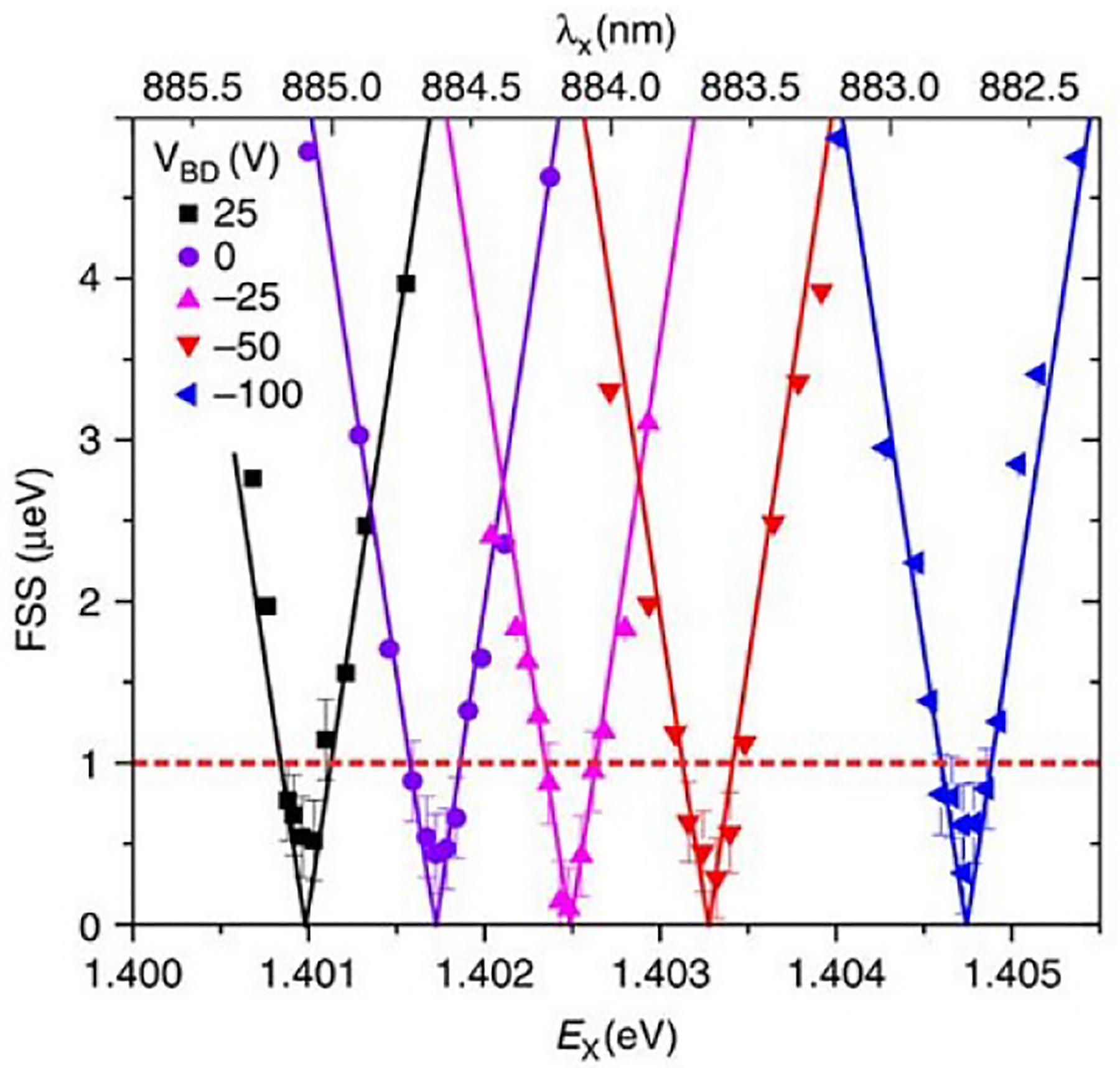
Sketch of FSS is plotted as a function of the exciton wavelength (energy), at different values of biased voltage VBD. The solid lines are theoretical fits. Exciton energy at which FSS ~0 is tuned by 3.7 meV. Reproduced with permission.[170] Copyright 2016, Springer Nature.
Strain engineering provides a dynamic way to modify the electronic and optical materials’ properties and has to date been explored to modify the optical properties of QDs. As the micro-piezo film tuning technique is naturally applicable to any thin-film quantum materials, application in a wide range of contexts is envisioned. For example, nanocavities deterministically fabricated around quantum emitters including atomic defects in solids offer a platform for the investigation of their interactions,[60, 172] especially when integrated with ‘the strain engineering knob’ to tune the coupling strength. Another example is the bandgap opening of graphene.[173] In summary, strain engineering with dynamic amplitude and direction control at cryogenic temperatures is a highly valuable technique to explore strain-dependent physics.
3.3. Quantum frequency conversion
Quantum frequency conversion (QFC), as its name suggests, is a technique developed to convert the frequency or wavelength of the quantum state of light while preserving its quantum properties.[174–176] When interfacing quantum sources such as QD single-photon emitters, QFC could serve as a versatile tool for many important applications. For example, one way to remove the spectral distinguishability among different QDs is to apply QFC, which brings the desired photons to the same wavelength without direct modification of the underlying QD sources.[175] As a result, the output photons may become indistinguishable, a prerequisite for a variety of quantum experiments. Moreover, QFC can translate the spectrum of QDs across disparate wavelength bands with high efficiency, allowing QDs to be interfaced other quantum nodes such as quantum memories, quantum channels as well as detectors at the wavelengths where the performance of such devices is optimized.[175]
Two key metrics of a quantum frequency converter are the conversion efficiency and the added noise. While the importance of high conversion efficiency is self-evident, the noise aspect is really what distinguishes the quantum frequency converters from their classical counterparts. This is because, in a classical frequency converter, the input signal is expected to be much stronger than processes which result in spontaneous photon (noise) generation. On the other hand, noise on the single-photon level is already comparable to the signal of the quantum frequency converter and must be minimized. For this reason, many classical frequency conversion techniques cannot be readily applied to quantum applications. Below, we will describe the major existing QFC technologies and discuss a few experiments relevant to the QD light sources.
Fundamentally, changing the frequency of a photon and hence its energy necessitates certain mechanism for energy exchange, as dictated by the law of conservation of energy. This typically involves the interaction of the signal photon with other entities such as photon(s), phonon(s), etc.[176, 177] One primary approach of QFC is based on nonlinear optics, where photons effectively interact with each other through the aid of a nonlinear medium.[176] Depending on the number of photons involved in the nonlinear interaction, these processes are ranked as second-order (three photons), third-order (four photons), and so on. Take the second-order nonlinear process for an example, the signal photon can mix with the pump photon to produce a third photon, whose frequency is either the sum or the difference of that of the signal and the pump. Normally, such nonlinear processes are quite weak unless the corresponding phase matching condition is satisfied. The role of phase matching in QFC is similar to momentum conservation in classical physics, which is to maintain a stable phase for the designated nonlinear term throughout the interaction process. In addition, to attain high conversion efficiencies, a relatively strong pump power well above the single-photon level is typically required. As such, the pump is almost exclusively treated as classical light.
One of the most common second-order nonlinear materials is lithium niobate. Because periodically poled lithium niobate (PPLN) waveguides offer a convenient platform for quasi phase matching (QPM), they have been a popular choice for QFC.[175] The periodic change of refractive index from poling results in an index grating and QPM is achieved by choosing a proper poling period to compensate the phase mismatch of the underlying process (see Figure 8(a)). Notably, the internal conversion efficiency of PPLN waveguides can be high (close to 100%), albeit at the cost of relatively strong pump power (on the order of a few hundred mW) and relatively large size (waveguide length on the order of cm). While in principle there is no intrinsic noise associated with the second-order process, whether it is sum or difference frequency generation, oftentimes there are background noise sources such as Raman noise induced by the strong pump. These noise sources typically exhibit a bandwidth much larger than that of the signal and can be suppressed by aggressive spectral filtering, provided that there is enough frequency separation between the signal and the pump.[175–178]
Figure 8.

(a) Illustration of the sum frequency generation in periodically poled lithium niobate (PPLN) waveguides. Quasi phase matching (QPM) is achieved by choosing the proper poling period to compensate the phase mismatch of the nonlinear process. Reproduced with permission.[175] Copyright 2012, American Institute of Physics. (b) Detection scheme based on quantum frequency conversion: single photons in the telecom band are upconverted to the visible range through efficient sum frequency generation and subsequently detected using silicon single-photon avalanche diode (SPAD). (c) Comparison of the two detection schemes for the telecom-band single photons: Direct detection using InGaAs single-photon detectors (left), and QFC-based detection scheme using SPAD (right). The detection dynamic range has been improved by a factor of 25. Reproduced with permission.[179] Copyright 2010, Springer Nature.
In the work by Rakher et al.,[179] single photons from an InAs/GaAs QD with an emission wavelength at 1300 nm were upconverted to 710 nm using a 1550 nm pump by implementing the sum-frequency generation in a PPLN waveguide. The frequency transduction from the telecom band to the visible spectrum enables the use of commercially available low-noise silicon detectors for efficient single-photon detection. Compared to the InGaAs/InP single-photon detectors typically used in the telecom band, silicon single-photon avalanche diode (SPAD) outperform them in terms of dark counts, dead time, and manufacturing cost. With an internal frequency conversion efficiency around 75% and quantum efficiency of SPAD around 70%, a total detection efficiency of 21% was realized at 710 nm after accounting for additional coupling losses.[179] Even though the overall detection efficiency is comparable to that of InGaAs/InP detectors for a direct detection of single photons at 1300 nm, the authors showed that the signal to noise ratio had been improved by a factor of 25 (see Figure 8(b)), demonstrating the superior performance of such QFC-based detection schemes.
Following the work by Rakher et al., Ates et al. adopted a similar approach to upconvert InAs/GaAs QD transitions in 980 nm to the 600 nm range using a 1550 nm pump laser.[180] Because of the wide spectral separation between the signal and the pump (> 600 nm in wavelength), the signal-to-background noise ratio exceeds 100:1, allowing the preservation of the single-photon characteristic in the converted photons. In addition, two spectrally separate QD transitions are converted to the same wavelength at 600 nm using a single PPLN waveguide (with energy difference compensated by two different 1550 nm pumps). As a result, the two single photons that were initially nondegenerate in the 980 nm band became degenerate in the 600 nm band, and nonclassical two-photon interference was observed.[180] Recently, a similar experiment was carried out for two InAs/GaAs QDs in the 900 nm band; but instead of upconversion, they were downconverted to the same wavelength in telecom band (1550 nm) using a 2157 nm pump.[181] This is particularly meaningful for long-distance quantum communication, since fibers have the lowest transmission loss in the telecom band and a vast body of infrastructures exists in this spectral window.[182, 183]
In addition to the second-order nonlinear processes, the third-order nonlinearity can also be employed for QFC. Suitable are, for example, centrosymmetric materials. However, the commonly used four-wave mixing process for classical frequency conversion, which relies upon parametric gain introduced by the pump, also amplifies the vacuum fluctuation noise and renders itself unfit for QFC.[184] On the other hand, there is another form of four-wave mixing, i.e., four-wave mixing Bragg scattering (FWM-BS), that is intrinsically noise-free.[184] As illustrated in Figure 9(a), the FWM-BS process requires two nondegenerate pumps, which effectively beat with each other and result in an active grating. The signal photon is then ‘scattered’ to two sidebands (in the frequency domain), one at a higher frequency and the other at a lower frequency, with the frequency shift determined by the frequency difference of the two pump lasers.
Figure 9.

(a) Scanning electron micrograph of a 40-μm-radius silicon nitride microresonator (left) and the schematic of the four-wave mixing Bragg scattering process implemented (right): the two pumps are in the 1550 nm band, while the signal and the frequency converted idlers are all in the 930 nm band. Reproduced with permission.[187] Copyright 2016, Springer Nature. The frequency translation is an integer number of the free spectral range of the microresonator. (b) The upper figure shows the signal transmission based on a swept tunable laser for several different pump powers, going from over coupling in the linear case (green line) to critical coupling (blue line) and finally under coupling (red dotted line) as the pump powers increase. The lower figure plots the output spectrum of the frequency converter with a 1 FSR separation between the two pump lasers (frequency translation ≈ 572 GHz) for a total pump power of 20 mW on-chip (10 mW each). The power in the 930 nm band is normalized by the input signal power, corresponding to the on-chip conversion efficiency for a narrowband input signal. Reproduced with permission.[188] Copyright 2019, American Physical Society.
While the first QFC experiment based on FWM-BS was realized in optical fibers, the frequency conversion process often suffers from strong Raman noise in silica unless cooled to very low temperatures (a few Kelvin).[185, 186] Furthermore, the size of such devices is typically on the order of meters due to the relatively weak nonlinearity of silica. Recently, silicon nanophotonics has emerged as a promising platform for the scalable implementation of a wealth of quantum technologies. Especially, FWM-BS designed to interface InAs/GaAs single photons sources has been successfully demonstrated in compact silicon nitride microresonators (diameter < 0.1 mm).[187] In this configuration, the two pumps reside in the 1550 nm band, while the signal and the two converted idlers are in the 930 nm band (Figure 9(a)). Such a large spectral separation between the signal and pumps minimizes the impact of background noises induced by the two pumps. As a result, the signal to background noise ratio can be on the order of 100:1 or higher.[187] One limitation of such resonator-based devices is that high conversion efficiencies can only be achieved when the signal bandwidth is sufficiently smaller than the conversion bandwidth, which is typically on the order of a few GHz. For example, a recent experimental study shows that the on-chip conversion efficiency for a narrowband signal comprised of attenuated laser light is more than 30% with a total on-chip pump power of 20 mW (See Figure 9(b)).[188] When replaced by single photons from QDs under p-shell excitation, however, the conversion efficiency drops to approximately 12%. This is because the QD emission has a bandwidth of around 2.9 GHz, which is larger than the 1.65 GHz bandwidth offered by the frequency converter.[188]
To summarize, we have discussed the major QFC technologies that are suitable for QD single-photon sources, including the second-order and third-order nonlinear processes. While material platforms such as PPLN and nonlinear fibers are quite mature and have been the mainstream choice for QFC, they face their own challenges such as the requirement of relatively strong pump power and relatively large device size, both of which make scaling an issue in future. On the other hand, the emerging silicon nanophotonics platform has shown some promises in implementing QFC in a scalable fashion and the possibility to integrate with other quantum nodes coherently. Being in the preliminary stage, however, further developments are needed to improve the conversion efficiency and to address the limitations imposed by the employment of microresonators.
4. Advanced QD Excitation Methods
In the previous sections, we have extensively discussed techniques used to engineer the spatial and spectral properties of QDs. To reliably achieve the desirable, indistinguishable single-photon emission from QDs, new optical excitation schemes are being developed to efficiently reduce the decoherence associated with phonon scattering processes and charge noises result in a fluctuating electric field in the solid.[189]
Figure 10 illustrates the energy configurations for optical excitation schemes commonly used for producing QD single-photon emission and the corresponding emission spectra.[190] On-demand single-photon generation from single QDs relies on pulsed laser pumping under such schemes, such that, ideally, a single photon created from a single QD exciton is produced at each excitation pulse.
Figure 10.

(a) (b) (c) Above-band resonant, quasi-resonant and resonant optical excitation schemes. (d) The spectrum of photons from above-band excitation. (e) The spectrum of photons from quasi-resonant excitation. (f) The Mollow-triplet spectrum of photons from resonant excitation. Reproduced with permission.[190] Copyright 2013, Science China Press.
The most straightforward method to populate QDs with excitons is through above-band optical excitation, or illumination with a laser at an energy higher than the bandgap of the QD-hosting semiconductor. In such a process (Figure 10(a)), carriers produced in the host conduction and valence bands relax via interactions with phonons, become trapped in the QD confinement potential, and form QD excited states. Such a process inevitably introduces significant decoherence and timing jitter in the single-photon emission from QD excitons,[189] evidenced by broad spectral linewidths as in Figure 10(d). Most bright energy levels of individual QD can be visualized via the PL spectra obtained through above-band excitation scheme at a high pumping power.[191]
Instead of pumping carriers directly across the semiconductor bandgap, the excited states of QDs can be selectively populated via quasi-resonant excitation, i.e., the excitation laser is resonant with high energy, p-shell excited states, as illustrated in Figure 10(b).[192, 193] Compared with above-band optical excitation, this technique effectively reduces the interaction between the carriers and phonons, thus reducing decoherence-causing processes, leading to narrower linewidths for emitted photons, as shown in Figure 10(e).[194, 195] In addition, each QD has a unique p-shell energy associated with its physical size/shape and material composition due to the randomness of the self-assembly growth process.[196] As such, p-shell excitation was widely used in early QD cavity QED experiments to selectively address targeted QDs in high-density samples, in which multiple dots could exist within the spot of the excitation laser.
While quasi-resonant pumping leads to significantly narrow emission linewidths, utmost coherent emission can be achieved through resonant excitation in the s-shell.[197] By tuning the excitation laser to the emission energy of a QD exciton transition (Figure 10(c)), the exciton state can be directly and coherently populated, without phonon processes and strong charge fluctuations that may introduce further decoherence. Generation of highly-coherent single-photons on demand through resonant excitation has been implemented in solid-state systems through QDs.[65, 198] Rabi oscillations[199] in the time-domain and the characteristic Mollow triplet in the spectral domain (Figure 10(f)) have been demonstrated.[200, 201] The main challenge to implementing resonant excitation lies in effectively distinguishing resonance fluorescence signals and backscattered excitation laser, which is usually achieved by separating the collection and pump paths into either two orthogonal spatial directions[64, 202] or polarizations.[203, 204] For example, in the former scheme, a QD-containing micro-pillar or planar cavity can be illuminated from side, while the QD resonance fluorescence that is vertically emitted into free-space is collected above such structures. Here, a 5% resonant pump suppression can be achieved by exciting the micro-pillar or the planar cavity from the side and detecting resonance fluorescence from the top.[205] Alternatively, a signal-to-noise ratio of up to 300 for resonance fluorescence over the excitation laser is routinely achievable by preparing the excitation laser in one linear polarization and collecting emission at the orthogonal linear polarization. Figure 11 illustrates the schematics of different setups used for non-resonant and resonant excitation. An important issue with resonant excitation is that the efficiency of populating the QD exciton state is very sensitive to variations of both the pump pulse area and the dipole moment of the QDs. To overcome this challenge, adiabatic rapid passage (ARP) with frequency-chirped pulses was developed by Wei et al. to stably generate single-photons with indistinguishability up to 0.995, with insensitivity to laser power variations.[206] The power and time-dependent resonance fluorescence count rates are shown in Figure 12.[206]
Figure 11.

(a) Setup of the confocal microscopy without polarization suppression.[204] Copyright 2019, American Chemical Society. (b) The confocal microscopy setup with polarization suppression for resonant excitation.[204] Copyright 2019, American Chemical Society. (c) Schematic for orthogonal excitation and detection.[202] Copyright 2007, American Physical Society.
Figure 12.
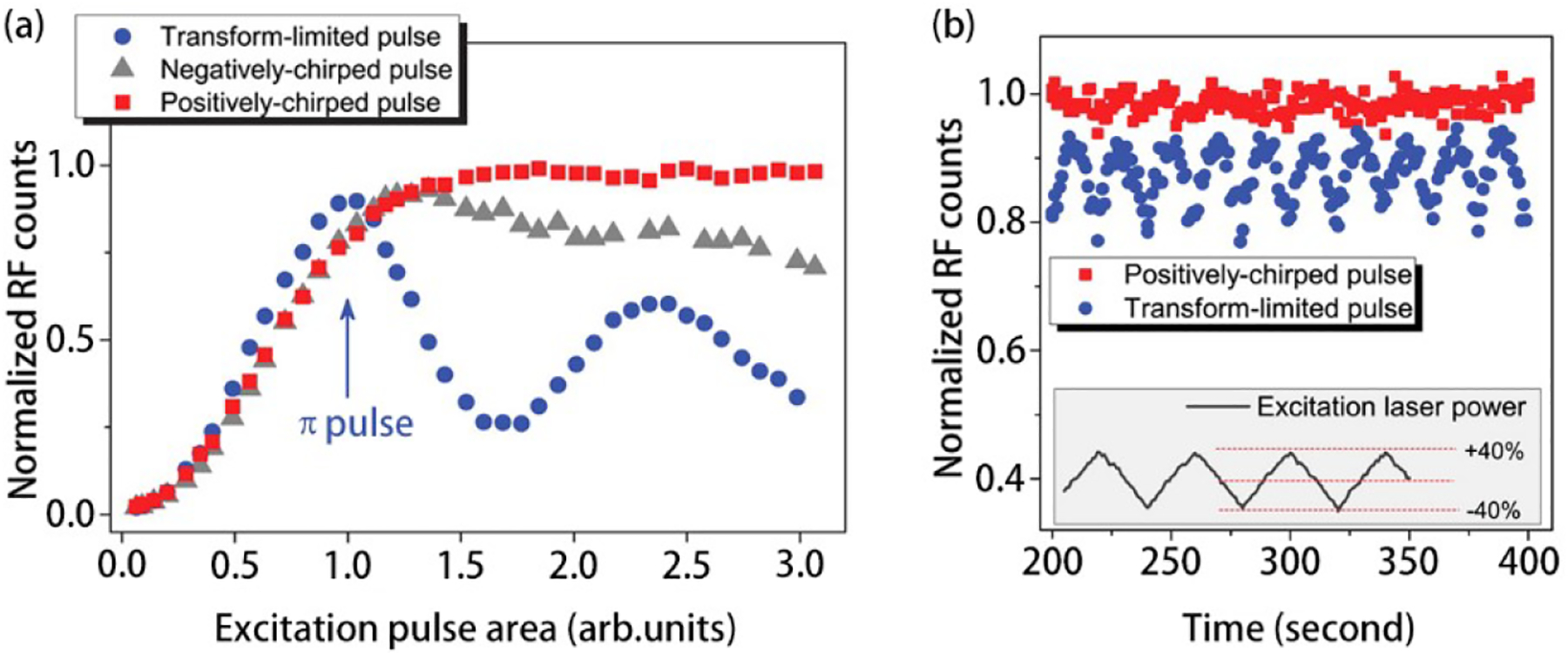
(a) Power-dependent resonance fluorescence count rate for three different excitation methods. (b) Time-dependent resonance fluorescence count rates under external modulation of laser power as indicated by the dark line in the inset. Reproduced with permission.[206] Copyright 2014, American Chemical Society.
Generation of entangled photon pairs can be achieved through cascaded emission from the biexciton (XX) and neutral exciton (X) states, following high-fidelity preparation of the QD into the XX state.[207, 208] Here, rather than preparing the QD in the X state by absorption of one photon from the excitation laser, the XX state can be prepared very effectively via a resonant two-photon excitation (TPE) process, in which the pump laser is tuned to half of the biexciton energy.[132, 209] Thanks to the Coulomb interaction between the QD-confined charges, the X energy is typically separated from the XX energy by a few meV. The pump laser energy is thus not resonant with either line and can be effectively suppressed with sharp notch filters.[72, 103] Recent studies have shown that the X and XX can be coherently populated with near-equal efficiencies, showing entanglement fidelities comparable to that of SPDC sources.[210] Similarly to ARP, the pulse shape of the TPE can be carefully engineered to improve the robustness of the XX preparation against laser power and frequency fluctuations, see Figure 13.[210] Very recently, phonon-assisted TPE was also demonstrated to be a very robust technique to prepare XX for generating entangled photon pairs, and was used to demonstrate interference of single-photons from separate QDs.[211]
Figure 13.

(a) Spectrum of a GaAs QD under phonon-assisted two-photon excitation for optical detuning of the laser energy and pulse length. Reproduced with permission.[211] Copyright 2017, American Chemical Society. (b) Power dependent studies of the resonant TPE. The results of the phonon-assisted excitation scheme are shown as green circles. Reproduced with permission.[211] Copyright 2017, American Chemical Society. (c) The ratio of the experiment data: 2X/X. Reproduced with permission.[210] Copyright 2017, American Physical Society.
Moving forward, it would be highly desirable to replace optical pumping with the electrical injection to address targeted transitions of the QD states, especially when large scale device integration is needed. Controlling the energy of electrically injected carriers is highly challenging, and so far direct coherent preparation of QD excitons through electrical injection has not been demonstrated. On the other hand, fabricating electrically injected nanolasers on-chip is becoming feasible through both dielectric and plasmonic structures[212–215]. Therefore, a compromise approach towards electrical resonant excitation is to electrically drive an on-chip nanolaser device that is resonant with the targeted QD energy level. Due to the low excitation power required for optically exciting single QDs, an electrically injected nanolaser could be powerful enough for on-chip excitation. Such a possibility has been realized with an elegant proof of concept experiment in which an electrically injected QD-based micropillar laser was used to resonantly excite the single QDs embedded in an adjacent micropillar.[216] Nonetheless, despite the great technological challenges realizing efficient electrical resonant excitation can still be envisioned in the future QD quantum photonic experiment through advanced device design and fabrication processes.[217, 218]
5. Heterogeneous integration for quantum photonics
The development of integrated quantum or classical photonic devices can greatly benefit from the ability to incorporate different types of materials with complementary, superior optical or electrical properties on a single chip.[54] Heterogeneous photonic integration, or the combination and processing of different materials on the same photonic chip, enables the creation of highly functional integrated photonic devices, with highly optimized performance. Such a capability is crucial for a wealth of quantum photonic applications (quantum networks,[219] quantum simulation,[220] and quantum sensing and metrology[21]), which require high on-chip single-photon generation rates, minimal losses in photon propagation, routing, and interferometry, highly efficient single-photon detection and fast and low-loss photonic switching.
In particular, self-assembled III-V QDs are currently the most all-around mature single-photon single solid-state emitters,[221] having been centrally employed in close-to-optimal triggered single-photon sources,[64, 65] spin-qubit interfaces,[222] and cavity quantum electrodynamics (cQED) systems.[223–225] The ability to implement such capabilities within an integrated quantum photonic circuit chip can be widely enabling towards quantum photonic applications. It would allow, for instance, large fluxes of indistinguishable single-photons to be launched with minimal losses into an on-chip waveguide-based interferometric network, as depicted in Figure 14(a),[226] which is essential for the boson sampling type quantum simulation.[227] Considerable effort has been made towards the creation of photonic integrated circuits that incorporate both self-assembled dots and passive waveguiding structures in purely III-V materials recently reviewed by Dietrich et al.;[26] The work by Schwartz et al. provides an outstanding example, where single-photon detectors are monolithically integrated, such an approach imposes a challenging trade-off between the achievable on-chip light-matter interaction and photonic losses.[228] The former factor regards the ability to couple quantum dot emission into manageable optical modes (e.g., a single on-chip waveguide or cavity mode), and can be substantially enhanced in carefully designed III-V semiconductor geometries; the latter regards the ability to transport and interfere emitted photons on-chip with minimum photon losses (e.g., in a large interferometric network that implements a unitary transformation), and is in general difficult to be minimized in etched III-V geometries. Such trade-off, discussed in more depth by Davanco et al., can be significantly relaxed by introducing an alternative material onto the chip, with which lower propagation losses can more easily be achieved.[226] For instance, while the lowest reported propagation losses in QDs-free GaAs waveguides have to date remained in the several dB/cm range,[26] and cavities with quality factors exceeding 106 have only recently been demonstrated, albeit at telecom wavelengths,[229] weakly-guiding Si3N4 waveguides demonstrated propagation losses of < 0.1 dB/m,[230, 231] and cavities with quality factors > 107.[232] Indeed, most quantum photonic chips of significant complexity demonstrated to date have been produced in single material systems with which reliably low propagation losses could be achieved - e.g., silica,[233] high-index dopes silica,[234] Si3N4,[235] silicon-on-insulator-,[236] but which did not offer deterministic light-generation capabilities. It is worth noting that, while heralded single-photon generation via spontaneous four-wave-mixing is possible in many such platforms, such probabilistic process offers limited single-photon generated rates due to a fundamental trade-off with multi-photon generation probabilities.[65] Also worth noting is the fact that Si3N4 offers additional desirable properties, complementarily to GaAs, which can create new device functionality - for instance, relatively pronounced Kerr nonlinearities and absence of two-photon absorption may allow quantum frequency conversion in on-chip nanophotonic cavities.[187]
Figure 14.

(a) Conceptual quantum photonic circuit composed of a waveguide interferometric network with a directly integrated GaAs nanophotonic device containing a single InAs quantum dot. The zoomed-in image of the GaAs device region (inside the dashed boundary box) shows details of the geometry and operation principle. The light-matter interaction section of the device promotes efficient coupling between the InAs quantum dot and a confined optical mode (here, a wave confined in a GaAs waveguide). Adiabatic mode transformers allow light from the QD in the light-matter interaction region to be efficiently transferred to a Si3N4 waveguide. (b) Fabrication process in the wafer-bonding approach. The bonded GaAs / Si3N4 wafer is shown inside the dotted line, schematically at the top, and imaged in a cross-sectional scanning electron micrograph. After wafer bonding, two subsequent electron-beam lithography and etch steps (first the GaAs layer, then the Si3N4) are used to define the geometry in (a). (c) GaAs microring resonator coupled to a GaAs bus waveguide terminated into mode transformers fabricated through the process in (b). (d) Photoluminescence spectrum for the microring in (c), showing single quantum dot transition coupled to a whispering-gallery mode. Inset: second-order correlation showing antibunching characteristic of single-photon emission. Reproduced with permission.[226] Copyright 2017, Springer Nature.
The first report of hybrid integration of quantum dot-based singe single-photon sources on the low-loss silicon-based photonic circuit was by Murray et al.[237]. Here, a bare strip of a GaAs wafer containing InAs QDs was orthogonally bonded to the cleaved facet of a Silicon Oxynitride (SiON) waveguide-based Mach-Zehnder interferometer (MZI). Coupling of quantum dot single-photons into one of the MZI input waveguides relied on the chance spatial alignment of an individual dot to the former; without shaping of the GaAs to help funnel quantum dot emission into the input waveguide, a theoretical maximum collection efficiency of about 3% was predicted. Following this initial demonstration, incorporation onto silicon-based photonic circuits of III-V nanophotonic geometries designed for enhanced collection efficiency has so far been explored primarily through two different approaches - one based on wafer-bonding,[226] and one based on pick-and-place techniques.[238–242]
5.1. Wafer bonding approach
This approach involves an initial step in which two wafers of different materials are brought together, so that device fabrication can subsequently follow a single high-throughput process flow with top-down fabrication techniques. Such an approach has indeed been employed highly successfully in the creation of heterogeneous integrated photonic circuits for classical photonics applications, most notably the creation of silicon photonic devices such as lasers and transceivers with optical gain provided by III-V materials.[243] One of the main advantages of such an approach is in scalability – it allows wafer-scale device production by leveraging the massive parallelism enabled by mature, top-down semiconductor fabrication methods. As discussed below, though, scalability meets a challenging bottleneck in integrated photonic devices with single QDs.
Whereas quantum dot lasers produced on silicon substrates through a direct wafer fusion bonding process were demonstrated by Tanabe et al.,[244] Davanco et al.[226] showed that direct wafer bonding could be leveraged to produce Si3N4 waveguide-based photonic circuits incorporating single QDs as single-photon sources. Here, a heterogeneous GaAs/Si3N4 stack was produced with a low temperature, oxygen plasma-activated wafer bonding procedure that had been previously shown to produce silicon photonic lasers with InP-based quantum well gain media.[245] The stack, shown in Figure 14(b), consisted of a silicon substrate covered by 3 μm of thermal SiO2, 550 nm of stoichiometric Si3N4 produced through low-pressure chemical vapor deposition (LPCVD), and a ≈ 200 nm thick layer of GaAs containing InAs QDs at half thickness. We note that thick LPCVD Si3N4 is known to provide high quality, low loss and dispersive propagation suitable for on-chip nonlinear optics.[187] After wafer bonding, fabrication proceeded through two subsequent, aligned electron-beam lithography and etching steps, as seen in Figure 14(b). This method affords nearly independent, flexible, and high-resolution tailoring of both active (GaAs) and passive (Si3N4) photonic waveguide elements with precise and repeatable, sub-100 nm alignment defined lithographically.
Such a capability maximizes the potential for implementation of high photonic performance through highly optimized geometries in both material layers. GaAs geometries such as nanowaveguides, waveguide-coupled microring or microdisk resonators, or 1D photonic crystals have all been implemented.[226] All of these structures can be used to enhance the coupling between GaAs-confined photonic modes (e.g., waveguide or resonant cavity modes) and embedded InAs QDs. Such coupling is quantified through the β-factor parameter or the percentage of the total emitted power that is carried by a desirable photonic mode. Importantly, the refractive index contrast between GaAs and Si3N4 is sufficiently high to allow optical modes that are highly confined in the GaAs layer, despite the presence of the Si3N4 substrate, allowing high (> 90%) β-factors comparable to those achieved in equivalent suspended GaAs structures.[246, 247] At the same time, light extraction from such nanostructures into the underlying Si3N4 waveguides can be efficiently (> 95%) done through adiabatic mode transformer geometries, implemented through carefully tailored tapered-profile coupled waveguides in both GaAs and Si3Ns layers. Nanometer-scale geometry control is crucial in both cases.
Figure 14(d) shows one of such geometries, a GaAs microring resonator of diameter 20 μm, formed by 300 nm wide GaAs waveguide containing InAs QDs, evanescently coupled to a GaAs bus waveguide. The latter is terminated into tapered adiabatic couplers, which efficiently transfers light between the GaAs and Si3N4 waveguides. A Purcell radiative rate enhancement of about 4 (from a theoretical 6) was demonstrated for a quantum dot coupled to a microring whispering-gallery mode with a large mode volume of ≈76 cubic wavelengths, and quality factor Q ≈ 6×10³.
A foremost issue with the wafer bonding approach is that considerable effort is required for bringing two materials together before device fabrication can even be considered. A further issue, after the two materials are bonded, is that sub-optimal device performance may arise due to process incompatibility. Increasing the complexity to more than two types of materials on one chip is furthermore challenging. Finally, although the wafer bonding approach allows high-throughput wafer-scale device production, a challenging bottleneck exists on the path towards single quantum dot devices. Self-assembled epitaxial QDs, currently the most mature class of single-photon emitters, are produced in the Stranski-Krastanow growth mode, which offers limited ability to control the spatial location and dipole moment orientation, emission wavelength and excited state coherence of individual dots within a single wafer.[221] As a result, highly optimized single-photon sources based on single QDs can only be produced after extensive search and characterization of individual dots across the wafer, as well as precise device placement around selected emitters. Various techniques, e.g., in situ EBL approach, have been developed to position and characterize individual QDs on a wafer surface, and then produce nanophotonic geometries that contain and are deterministically positioned to selected dots.[58, 248–255] Although under the wafer-bonding approach devices produced in this fashion would end up randomly distributed across the wafer, according to the random positions of the selected dots - which would require ad-hoc design of the Si3N4 waveguide network-, high-throughput QD positioning is a viable workaround towards scalable fabrication of single-dot device networks.
5.2. Pick-and-place approach
In the pick-and-place approach, different components of a device, composed of different materials, are produced separately and in parallel through well-developed fabrication techniques, and then brought together through a lower-throughput mechanical transfer process. Here, greater scalability is sacrificed in favor of processing flexibility and fast turn-around. Individual device performance can be better optimized within the respective, parallel runs. In addition, high-performing devices within a large population produced by low-yield methods can be selected and transferred to a final chip.[256] While the technique is particularly attractive for rapid device prototyping and proof-of-principle demonstrations, agile automation can potentially lead to significant gains in device scalability. Importantly, the lack of deterministic control over self-assembled quantum dot growth location is, likewise to the wafer bonding approach, a challenging scalability bottleneck for pick-and-place based device fabrication.
In the work by Zadeh et al., pick-and-place was used to produce hybrid devices as shown in Figure 15(a), composed of InP nanowires, containing single InAsP QDs, which were embedded in SiN waveguides.[239] The high index contrast between the InP and SiN helped promote high collection efficiency for quantum dot-emitted photons into a confined InP waveguide mode, and a slight tapering of the NW tip, with geometry controllable through growth parameters, allows efficient launch of dot emitted photons into the SiN waveguide, with a theoretical maximum of 36%. The III-V nanowire and QD were grown by a selective-area and vapor-liquid-solid epitaxy process,[129] which produced microns-long, roughly 100 nm-wide upright standing wurtzite nanocrystals. These nanocrystals were plucked from the growth substrate using a tungsten tip mounted on a 3-axis movable stage, and through imaging with an optical microscope transferred to a silicon chip with <500 nm position and <2 degrees rotation precision. The receiving chip consisted of a Si wafer covered by a 2.4 μm SiO2 film, which served as a low-index substrate layer, and featured prefabricated markers used to align the photonic circuits with respect to the NWs. The sample was covered in SiN grown by plasma-enhanced chemical deposition (PECVD), and lithography and etching of the SiN were used to define the photonic circuits. The experimental source efficiency was of about 24%. The nature of the NW growth is such that QDs are naturally aligned to such nanophotonic structure, which saves considerable overhead in the production for wire sources with maximized performance. On the other hand, reduced freedom in choosing the III-V nanophotonic geometry, as opposed to that achievable through lithography and etching, creates challenges towards achieving further desirable features, such as maximized unidirectional emission and Purcell radiative rate enhancement. Filtering of quantum dot emission by on-chip SiN microring resonator filters under this platform was demonstrated by Elshaari et al.[241]
Figure 15.

Schematics of hybrid photonic circuit platforms produced through pick-and-place techniques, including passive waveguides and quantum dot-based nanophotonic single-photon sources. (a) InP NW containing InAsP QD, encapsulated in a SiN waveguide and capped with a layer of polymethyl acrylate (PMMA). The nanowires were produced through a selective-area and vapor-liquid-solid epitaxy process.[129] Reproduced with permission.[239] Copyright 2016, American Chemical Society. (b) InP nanobeam with embedded InAs QDs, placed above a Si waveguide on a SiO2 waveguide. Reproduced with permission.[240] Copyright 2017, American Chemical Society. (c) GaAs photonic crystal cavity containing InAs QDs, placed over a GaAs waveguide on a SiO2 substrate, spaced from it by distance d, by way of a planarized spin-on-glass (SOG) layer. Reproduced with permission.[242] Copyright 2018, Optical Society of America. (d) Schematic of quantum memories based on diamond nanobeams with NV centers, coupled to SiN waveguides. Reproduced with permission.[238] Copyright 2014, American Physical Society. (e) Right panel: illustration of NbN superconducting nanowire single-photon detector on a SiN membrane being transferred onto a silicon-on-insulator photonic waveguide. Right panel: Schematic of a photonic chip with four waveguide-integrated detectors (A1, A2, B1 and B2). Reproduced with permission.[256] Copyright 2015, Springer Nature.
In the work by Kim et al.[240], pick-and-place was carried out in a focused ion beam (FIB) system to produce hybrid devices as depicted in Figure 15(b), consisting of an InP nanobeam containing InAs QDs (for emission in the 1300 nm telecom band), on top of a Silicon-on-insulator (SOI) photonic waveguide splitter. Both III-V and SOI samples were produced in separate runs, and a microprobe manipulator within the FIB was used to separate the nanobeam devices from the III-V substrate, then transfer them to the silicon chip. In contrast with the nanowire-based platform of Zadeh et al. and Elshaari et al.[239, 241] quantum dot-containing nanobeam geometries were produced through lithography and etching steps, and QDs were not deterministically positioned to the nanobeam geometry. An outcoupling efficiency of 32% was theoretically predicted into the Si waveguide, for an ideally positioned quantum dot (β=71% of quantum dot emission into the nanobeam’s fundamental TE guided mode, and coupling efficiency of 45% from such guided mode to the silicon waveguide, through an adiabatic mode transformer).
In the work by Katsumi et al.[242], InAs quantum dot-containing GaAs nanobeam photonic crystal cavities evanescently coupled to underlying GaAs waveguides were produced through a transfer-printing process.[257] Here, a Polydimethylsiloxane (PDMS) stamp was used to lift suspended GaAs nanobeams from a processed GaAs wafer. As shown in Figure 15(c), the destination substrate consisted of GaAs-on-SiO2 wafer onto which GaAs ridge waveguides were etched, covered by a spin-on-glass (SOG) top cladding. The SOG planarity and thickness was sufficient to, respectively, allow a clean transfer of the nanobeams from the PDMS stamp, and fine control of the coupling regime between the cavity and the underlying GaAs waveguide. Because PDMS is a transparent elastomer, high magnification microscopy imaging of both the lifted nanobeam and the waveguide on the final substrate was possible during the transfer process, which allowed positioning to within 100 nm. The small mode volume (≈ 0.5 cubic wavelengths) of the designed nanobeam photonic crystal cavity’s fundamental mode allows β-factors of ≈ 99% to be achieved, primarily through Purcell radiative rate enhancement, even for loaded quality factors Q in the few thousands. Importantly, Q is dictated by the coupling rate between the cavity and the waveguide, which is determined by the vertical distance d between the two. Although the coupling efficiency into the waveguide can be limited by parasitic losses to radiative modes as the distance d between guide and cavity goes below a certain point, efficiencies in excess of 99% are still achievable theoretically. Experimentally, the estimated emitter–cavity coupling efficiency was β ≈ 87%, the cavity-waveguide coupling efficiency was η ≈ 72%, for a total single-photon launch efficiency of ≈ 63% into the GaAs waveguide. Similar performance was also predicted for Si3N4 and Si waveguides.
Importantly, because in the pick-and-place approach the different material components of a finalized heterogeneous photonic chip are processed in separate runs, fewer issues with process compatibility can be expected, in comparison with a wafer bonding approach. This endows the technique with a great degree of flexibility, offering a low barrier towards the incorporation of different types of materials together. As an example, in the work by Mouradian et al.,[238] integration of quantum memories based on nitrogen-vacancy center defects in diamond nanobeam waveguides onto SiN waveguides (Figure 15(d)) was demonstrated using a similar pick-and-place process, employing micro-manipulation of tungsten tips, as for the InP nanowires with embedded InAsP QDs of Zadeh et al.[236] and Elshaari et al.,[237] described above. Similarly, Najafi et al.[256] also demonstrated the integration of niobium niobate superconducting nanowire single-photon detectors (SNSPDs), produced on SiN membranes, over an SOI-based photonic circuit (Figure 15(e)). Pick-and-place techniques also present a lower barrier for creating maximally performing devices based on components fabricated with low-yield processes, by allowing pre-screening and selection of the best performers within a population. Such capability was indeed leveraged in the diamond NV center quantum memories of Mouradian et al.[238], given that consistent, desired spectral and spin properties of fabricated nanobeams that contain inhomogeneous populations of NV centers are difficult to achieve. Similarly, Najafi et al.[256] produced an integrated photonic circuit chip for photon correlation measurements, containing 10 low-jitter SNSPD detectors with consistent timing jitter below 60 ps and detection efficiency between ≈14% and ≈52%.
Outlook
As discussed in the previous Sections, considerable progress has been made towards control and utilization of individual QDs in integrated photonic devices. Most current studies, however, regard only individual or small numbers of QDs, generally featuring those with exceptional characteristics. If the full potential for scalability offered by QDs as emitters in quantum photonic systems is to be realized, methods to produce or identify large numbers of high-quality QDs must be developed. It is arguable that further development of growth techniques may yield highly homogeneous populations of high-performance QDs; however, given the fact that even small variations in a variety of QD parameters - size, shape, strain, composition - can lead to significant variations in spectral and other relevant optical properties, it is likely that methods to deal with such variation post-growth will still be necessary. Further, even before post-growth techniques for spatial and spectral quantum dot control are applied, the search and identification, within a large as-grown population, of individual QDs that offer desirable characteristics will likely remain a crucial aspect of quantum dot device fabrication. Whereas single QD search and identification is already carried out in the various types of quantum dot positioning setups developed for deterministic single QD device fabrication,[258] achieving scalability in QD device fabrication will likely require not only automation, but also high-throughput spectral and quantum optical (i.e., single-photon purity, indistinguishability, level of entanglement, etc.) characterization of large numbers of individual dots within a grown ensemble. The latter capability may in addition be used to extract statistical information about a grown quantum dot population, which may provide valuable information for better growth process controls.
Beyond growth and QD characterization and selection, the inclusion of single QDs in appropriately designed photonic structures is crucial for the efficient utilization of emitted photons. Such structures can be effectively leveraged to funnel emission into selected, desirable spatial modes of a quantum photonic system, and therefore play an important role in system efficiency and, ultimately, scalability. Careful consideration must be paid to design and fabrication of the photonic structure, so that the geometry and the necessary fabrication process minimally affects the as-grown quantum dot optical properties. In particular, the close proximity of QDs to etched surfaces has been shown to induce significant linewidth broadening, and therefore coherence degradation, of QD transitions.[258, 259] In view of the necessity to adjust QD spectral properties, photonic design must accommodate QD tuning and stabilization methods, such as though mechanical strain and the DC Stark tuning; or, conversely, special consideration must be taken when implementing such tuning techniques against devices produced on a chip, so that photonic performance is minimally affected. Importantly, integration of quantum dot-containing devices onto heterogeneous photonic circuits is desirable as such type of integration leverages advantages of diverse types of materials to create devices with highly optimized performance. Such an approach may prove necessary in the development of chip-based quantum photonic quantum systems, given the demanding levels of efficiency that must be achieved in the generation, manipulation, and detection of quantum light. In particular, frequency conversion of single photons emitted by on-chip QD sources directly integrated onto χ(3) nonlinear nanophotonic devices such as discussed in Section 3.4, could be envisaged under this approach.
The careful photonic design will also likely be necessary for the on-chip implementation of the advanced optical pumping schemes described in Section 4, which aim at the production of perfectly indistinguishable photons. For instance, resonant pumping, via a free-space beam, of a QD embedded in a photonic circuit may lead to considerable scatter of the resonant pump light into the same waveguide into which resonance fluorescence photons are produced.[258] Alternative geometrical configurations for pumping and pump filtering[216] will likely have to be considered, alongside the abovementioned QD control features.
In summary, as may be gathered from this outlook discussion, the development of scalable photonic devices that fully leverage the advantages of multiple, individually operated quantum dots is a complex engineering problem, featuring multiple challenges regarding diverse aspects that must be met simultaneously. Importantly, many such challenges will exist in the development of quantum photonic device technologies that rely on any kind of solid-state quantum emitter. In this respect, quantum dots are advantageous due to their technological maturity.[221] This is evidenced by the various advanced techniques we have discussed in this review, which have been developed over many years of focused research, and which will likely feature in future QD based photonic devices.
Acknowledgements
The authors gratefully acknowledge financial support from National Key R&D Program of China (2018YFA0306100), the National Natural Science Foundations of China (11874437,11704424), the Natural Science Foundation of Guang-dong Province (2018B030311027, 2017A030310004, 2016A030310216) and Guangzhou Science and Technology project (201805010004).
Biographies

Jin Liu is a professor of physics in Sun Yat-Sen University. He obtained his PhD degree in 2012 from Technical University of Denmark in department of photonic engineering. Before moving back to China, he worked with Dr. Kartik Srinivasan at National Institute of Standards and Technology (NIST) to develop integrated quantum photonic circuits. His current research activities cover integrated quantum photonics and nanophotonics by utilizing molecular beam epitaxy, semiconductor nanofabrication and cryogenic optical characterizations.

Marcelo Davanco is a Scientist at the National Institute of Standards and Technology. He has B.S. and M.S. degrees in Electrical Engineering from the State University of Campinas, Brazil, a Ph.D. in Electrical and Computer Engineering from the University of California, Santa Barbara. Marcelo was a postdoctoral fellow at the University of Michigan and then at NIST. His current research interests are in heterogeneous integrated photonics with single quantum emitters.

Ying Yu received her PhD degree in Condensed Matter Physics from the Institute of Semiconductors, Chinese Academy of Sciences, China, in 2014. She is currently an associate professor in School of Electronics and Information Technology at Sun Yat-sen University, Guangzhou, China. Her research is mainly focused on the self-assembled III-Vquantum dots, nanocavities (nanowire, micropillar) and their applications in laser and quantum light sources.
Appendix. The Pikus-Bir Hamiltonian in semiconductor
In this appendix, we give a brief introduction of the theory of the strain-induced Hamiltonian known as the Pikus-Bir Hamiltonian to describe strain effects on the semiconductor band structure.[153, 154]
The strain is a dimensionless tensor, consisting of a set of coefficients ϵij with symmetric property, i.e. ϵij = ϵji where i, j are the coordinate indices
The strained crystal deforms according to a deformed lattice vector. Suppose the deformation is uniform. The relationship between the final (primed) and initial (unprimed) lattice vectors is expressed as
The relative crystal volume change is obtained by
In a III-V semiconductor, the conduction band is non-degenerate and only reacts to hydrostatic strain.[260] The deformation potential is defined as
where Ec is the conduction band energy. The conduction band energy shift is, therefore,
Similarly, we can obtain the valence band energy shift, caused by the hydrostatic
It is worth noting that the uppermost valence bands are two-fold degenerate. One is the heavy hole (HH) band , where jh represents the total angular momentum; jh,z is the projection on z axis. The other one is called the light hole (LH) band . Besides, there exists a third valence band with , caused by spin-orbit interaction. This band plays a minor role as it is usually hundreds of meV lower than the HH and LH bands. The effect of strain on these three valence bands is complex.
The Hamiltonian of a semiconductor is usually calculated by the k · p method. For an unstrained semiconductor, the Hamiltonian for the valence bands given in the basis of () reads as follows:
where γi (i = 1,2,3) are the Luttinger parameters, which describe the valence band curvatures. Δ is the energy splitting due to the spin-orbit interaction. ħ is max-planck constant. m0 is the mass of the hole and ki(i = x, y, z) is the wavevector. The strain-induced Hamiltonian known as the Pikus-Bir Hamiltonian can be obtained by using the coordinate transform method, as discussed at the beginning of the Section. At the Brillouin zone center, the strain Hamiltonian is given by:
where b and d are the Pikus-Bir shear deformation potentials for the valence band edge. For simplicity, we investigate the special case for biaxial strain where ϵxx = ϵyy and ϵxy = ϵyz = ϵxz = 0. The parameters Rϵ and Sϵ vanish. The Pikus-Bir Hamiltonian matrix becomes diagonal. The energy shifts of each valence band are given by the following eigenvalues:
It can be seen that the strain-induced energy shifts on LH and HH are different. Due to the built-in strain during the self-assembled process of QDs, the heavy- and light-hole states are split in energy by at least several tens of meV, with the HH states being the upper most states. However, the situation can be reversed by strain engineering as is demonstrated in Reference [261], where the LH states become the ground states.
References
- [1].O’Brien JL, Furusawa A, Vučkovič J, Nat. Photonics 2009, 3, 687. [Google Scholar]
- [2].Knill E, Laflamme R, Milburn GJ, Nature 2001, 409, 46. [DOI] [PubMed] [Google Scholar]
- [3].O’Brien JL, Science 2007, 318, 1567. [DOI] [PubMed] [Google Scholar]
- [4].Gisin N, Thew R, Nat. Photonics 2007, 1, 165. [Google Scholar]
- [5].Schmitt-Manderbach T, Weier H, Fürst M, Ursin R, Tiefenbacher F, Scheidl T, Perdigues J, Sodnik Z, Kurtsiefer C, Rarity JG, Zeilinger A, Weinfurter H, Phys. Rev. Lett 2007, 98, 010504. [DOI] [PubMed] [Google Scholar]
- [6].Ursin R, Tiefenbacher F, Schmitt-Manderbach T, Weier H, Scheidl T, Lindenthal M, Blauensteiner B, Jennewein T, Perdigues J, Trojek P, Ömer B, Fürst M, Meyenburg M, Rarity J, Sodnik Z, Barbieri C, Weinfurter H, Zeilinger A, Nat. Phys 2007, 3, 481. [Google Scholar]
- [7].Yin J, Ren J-G, Lu H, Cao Y, Yong H-L, Wu Y-P, Liu C, Liao S-K, Zhou F, Jiang Y, Cai X-D, Xu P, Pan G-S, Jia J-J, Huang Y-M, Yin H, Wang J-Y, Chen Y-A, Peng C-Z, Pan J-W, Nature 2012, 488, 185. [DOI] [PubMed] [Google Scholar]
- [8].Yin J, Cao Y, Li Y-H, Ren J-G, Liao S-K, Zhang L, Cai W-Q, Liu W-Y, Li B, Dai H, Li M, Huang Y-M, Deng L, Li L, Zhang Q, Liu N-L, Chen Y-A, Lu C-Y, Shu R, Peng C-Z, Wang J-Y, Pan J-W, Phys. Rev. Lett 2017, 119, 200501. [DOI] [PubMed] [Google Scholar]
- [9].Yin J, Cao Y, Li Y-H, Liao S-K, Zhang L, Ren J-G, Cai W-Q, Liu W-Y, Li B, Dai H, Li G-B, Lu Q-M, Gong Y-H, Xu Y, Li S-L, Li F-Z, Yin Y-Y, Jiang Z-Q, Li M, Jia J-J, Ren G, He D, Zhou Y-L, Zhang X-X, Wang N, Chang X, Zhu Z-C, Liu N-L, Chen Y-A, Lu C-Y, Shu R, Peng C-Z, Wang J-Y, Pan J-W, Science 2017, 356, 1140. [DOI] [PubMed] [Google Scholar]
- [10].Lv D, An S, Liu Z, Zhang J-N, Pedernales JS, Lamata L, Solano E, Kim K, Phys. Rev. X 2018, 8, 021027. [Google Scholar]
- [11].Georgescu IM, Ashhab S, Nori F, Rev. Mod. Phys 2014, 86, 153. [Google Scholar]
- [12].Lanyon BP, Hempel C, Nigg D, Müller M, Gerritsma R, Zähringer F, Schindler P, Barreiro JT, Rambach M, Kirchmair G, Hennrich M, Zoller P, Blatt R, Roos CF, Science 2011, 334, 57. [DOI] [PubMed] [Google Scholar]
- [13].Monz T, Nigg D, Martinez EA, Brandl MF, Schindler P, Rines R, Wang SX, Chuang IL, Blatt R, Science 2016, 351, 1068. [DOI] [PubMed] [Google Scholar]
- [14].Debnath S, Linke NM, Figgatt C, Landsman KA, Wright K, Monroe C, Nature 2016, 536, 63. [DOI] [PubMed] [Google Scholar]
- [15].Nielsen MA, Chuang IL, Quantum Computation and Quantum Information: 10th Anniversary Edition, Cambridge University Press, 2011. 708. [Google Scholar]
- [16].Degen CL, Reinhard F, Cappellaro P, Rev. Mod. Phys 2017, 89, 035002. [Google Scholar]
- [17].Budker D, Romalis M, Nat. Phys 2007, 3, 227. [Google Scholar]
- [18].Taylor JM, Cappellaro P, Childress L, Jiang L, Budker D, Hemmer PR, Yacoby A, Walsworth R, Lukin MD, Nat. Phys 2008, 4, 810. [Google Scholar]
- [19].Giovannetti V, Lloyd S, Maccone L, Science 2004, 306, 1330. [DOI] [PubMed] [Google Scholar]
- [20].Giovannetti V, Lloyd S, Maccone L, Phys. Rev. Lett 2006, 96, 010401. [DOI] [PubMed] [Google Scholar]
- [21].Giovannetti V, Lloyd S, Maccone L, Nat. Photonics 2011, 5, 222. [Google Scholar]
- [22].Müller M, Vural H, Schneider C, Rastelli A, Schmidt OG, Höfling S, Michler P, Phys. Rev. Lett 2017, 118, 257402. [DOI] [PubMed] [Google Scholar]
- [23].Kok P, Munro WJ, Nemoto K, Ralph TC, Dowling JP, Milburn GJ, Rev. Mod. Phys 2007, 79, 135. [Google Scholar]
- [24].Eisaman MD, Fan J, Migdall A, Polyakov SV, Rev. Sci. Instrum 2011, 82, 071101. [DOI] [PubMed] [Google Scholar]
- [25].Dowling JP, Contemp. Phys 2008, 49, 125. [Google Scholar]
- [26].Dietrich CP, Fiore A, Thompson MG, Kamp M, Höfling S, Laser Photonics Rev. 2016, 10, 870. [Google Scholar]
- [27].Bouwmeester D, Pan J-W, Mattle K, Eibl M, Weinfurter H, Zeilinger A, Nature 1997, 390, 575. [Google Scholar]
- [28].Wang X-L, Chen L-K, Li W, Huang HL, Liu C, Chen C, Luo YH, Su ZE, Wu D, Li ZD, Lu H, Hu Y, Jiang X, Peng CZ, Li L, Liu NL, Chen Y-A, Lu C-Y, Pan J-W, Phys. Rev. Lett 2016, 117, 210502. [DOI] [PubMed] [Google Scholar]
- [29].Yao X-C, Wang T-X, Xu P, Lu H, Pan G-S, Bao X-H, Peng C-Z, Lu C-Y, Chen Y-A, Pan J-W, Nat. Photonics 2012, 6, 225. [Google Scholar]
- [30].Lu C-Y, Zhou X-Q, Gühne O, Gao W-B, Zhang J, Yuan Z-S, Goebel A, Yang T, Pan J-W, Nat. Phys 2007, 3, 91. [Google Scholar]
- [31].Balić V, Braje DA, Kolchin P, Yin GY, Harris SE, Phys. Rev. Lett 2005, 94, 183601. [DOI] [PubMed] [Google Scholar]
- [32].Kolchin P, Du S, Belthangady C, Yin GY, Harris SE, Phys. Rev. Lett 2006, 97, 113602. [DOI] [PubMed] [Google Scholar]
- [33].Cho Y-W, Park K-K, Lee J-C, Kim Y-H, Phys. Rev. Lett 2014, 113, 063602. [DOI] [PubMed] [Google Scholar]
- [34].Smith BJ, Mahou P, Cohen O, Lundeen JS, Walmsley IA, Opt. Express 2009, 17, 23589. [DOI] [PubMed] [Google Scholar]
- [35].Fang B, Cohen O, Lorenz VO, J. Opt. Soc. Am. B 2014, 31, 277. [Google Scholar]
- [36].Freedman SJ, Clauser JF, Phys. Rev. Lett 1972, 28, 938. [Google Scholar]
- [37].Giustina M, Mech A, Ramelow S, Wittmann B, Kofler J, Beyer J, Lita A, Calkins B, Gerrits T, Nam SW, Ursin R, Zeilinger A, Nature 2013, 497, 227. [DOI] [PubMed] [Google Scholar]
- [38].Christensen BG, McCusker KT, Altepeter JB, Calkins B, Gerrits T, Lita AE, Miller A, Shalm LK, Zhang Y, Nam SW, Brunner N, Lim CCW, Gisin N, Kwiat PG, Phys. Rev. Lett 2013, 111, 130406. [DOI] [PubMed] [Google Scholar]
- [39].Brunner N, Cavalcanti D, Pironio S, Scarani V, Wehner S, Rev. Mod. Phys 2014, 86, 419. [Google Scholar]
- [40].Arakawa Y, Sakaki H, Appl. Phys. Lett 1982, 40, 939. [Google Scholar]
- [41].Huffaker DL, Park G, Zou Z, Shchekin OB, Deppe DG, Appl. Phys. Lett 1998, 73, 2564. [Google Scholar]
- [42].Huang X, Stintz A, Li H, Lester LF, Cheng J, Malloy KJ, Appl. Phys. Lett 2001, 78, 2825. [Google Scholar]
- [43].Shchekin OB, Deppe DG, Appl. Phys. Lett 2002, 80, 3277. [Google Scholar]
- [44].Chae W-S, Yun J, Nam S-H, Lee S-G, Yang W-G, Yoon H, Park M, Jeon S, ACS Appl. Mater. Interfaces 2018, 10, 14079. [DOI] [PubMed] [Google Scholar]
- [45].Bansal P, Khan Y, Nim GK, Kar P, Chem. Commun 2018, 54, 3508. [DOI] [PubMed] [Google Scholar]
- [46].Villa B, Bennett AJ, Ellis DJP, Lee JP, Skiba-Szymanska J, Mitchell TA, Griffiths JP, Farrer I, Ritchie DA, Ford CJB, Shields AJ, Appl. Phys. Lett 2017, 111, 011103. [Google Scholar]
- [47].Zavvari M, J. Opt. Soc. Am. B 2015, 32, 737. [Google Scholar]
- [48].Wong CH, Vavilov MG, Phys. Rev. A 2017, 95, 012325. [Google Scholar]
- [49].Yifat Y, Ackerman M, Guyot-Sionnest P, Appl. Phys. Lett 2017, 110, 041106. [Google Scholar]
- [50].Stevenson RM, Young RJ, Atkinson P, Cooper K, Ritchie DA, Shields AJ, Nature 2006, 439, 179. [DOI] [PubMed] [Google Scholar]
- [51].Schwartz I, Cogan D, Schmidgall ER, Don Y, Gantz L, Kenneth O, Lindner NH, Gershoni D, Science 2016, 354, 434. [DOI] [PubMed] [Google Scholar]
- [52].Schulte CHH, Hansom J, Jones AE, Matthiesen C, Le Gall C, Atatüre M, Nature 2015, 525, 222. [DOI] [PubMed] [Google Scholar]
- [53].Strauß M, Carmele A, Schleibner J, Hohn M, Schneider C, Höfling S, Wolters J, Reitzenstein S, Phys. Rev. Lett 2019, 122, 107401. [DOI] [PubMed] [Google Scholar]
- [54].Heidel ND, Usechak NG, Dohrman CL, Conway JA, IEEE J. Sel. Top. Quantum Electron 2016, 22, 482. [Google Scholar]
- [55].Heitz R, Ramachandran TR, Kalburge A, Xie Q, Mukhametzhanov I, Chen P, Madhukar A, Phys. Rev. Lett 1997, 78, 4071. [Google Scholar]
- [56].Löffler A, Reithmaier JP, Sęk G, Hofmann C, Reitzenstein S, Kamp M, Forchel A, Appl. Phys. Lett 2005, 86, 111105. [Google Scholar]
- [57].Bhattacharya P, Kamath K, Phillips J, Klotzkin D, Bull. Mater. Sci 1999, 22, 519. [Google Scholar]
- [58].Schnauber P, Schall J, Bounouar S, Höhne T, Park S-I, Ryu G-H, Heindel T, Burger S, Song J-D, Rodt S, Reitzenstein S, Nano Lett. 2018, 18, 2336. [DOI] [PubMed] [Google Scholar]
- [59].Unsleber S, He Y-M, Gerhardt S, Maier S, Lu C-Y, Pan J-W, Gregersen N, Kamp M, Schneider C, Höfling S, Opt. Express 2016, 24, 8539. [DOI] [PubMed] [Google Scholar]
- [60].Liu J, Su R, Wei Y, Yao B, Silva S. F. C. d., Yu Y, Iles-Smith J, Srinivasan K, Rastelli A, Li J, Wang X, Nat. Nanotechnol 2019, 14, 586. [DOI] [PMC free article] [PubMed] [Google Scholar]
- [61].Henini M, Brounkov PN, Polimeni A, Stoddart ST, Main PC, Eaves L, Kovsh AR, Musikhin YG, Konnikov SG, Superlattices Microstruct. 1999, 25, 105. [Google Scholar]
- [62].Ramachandran TR, Heitz R, Chen P, Madhukar A, Appl. Phys. Lett 1997, 70, 640. [Google Scholar]
- [63].Dieter B, Marius G, Nikolai NL., Quantum Dot Heterostructures, Wiley, New York; Jerusalem; London; Chichester: 1999. [Google Scholar]
- [64].Ding X, He Y, Duan ZC, Gregersen N, Chen MC, Unsleber S, Maier S, Schneider C, Kamp M, Höfling S, Lu C-Y, Pan J-W, Phys. Rev. Lett 2016, 116, 020401. [DOI] [PubMed] [Google Scholar]
- [65].Somaschi N, Giesz V, De Santis L, Loredo JC, Almeida MP, Hornecker G, Portalupi SL, Grange T, Antón C, Demory J, Gómez C, Sagnes I, Lanzillotti-Kimura ND, Lemaítre A, Auffeves A, White AG, Lanco L, Senellart P, Nat. Photonics 2016, 10, 340. [Google Scholar]
- [66].Kuhlmann AV, Prechtel JH, Houel J, Ludwig A, Reuter D, Wieck AD, Warburton RJ, Nat. Commun 2015, 6, 8204. [DOI] [PMC free article] [PubMed] [Google Scholar]
- [67].Wang H, Duan ZC, Li YH, Chen S, Li JP, He YM, Chen MC, He Y, Ding X, Peng C-Z, Schneider C, Kamp M, Höfling S, Lu C-Y, Pan J-W, Phys. Rev. Lett 2016, 116, 213601. [DOI] [PubMed] [Google Scholar]
- [68].Seguin R, Schliwa A, Rodt S, Pötschke K, Pohl UW, Bimberg D, Phys. Rev. Lett 2005, 95, 257402. [DOI] [PubMed] [Google Scholar]
- [69].Singh R, Bester G, Phys. Rev. Lett 2010, 104, 196803. [DOI] [PubMed] [Google Scholar]
- [70].Bester G, Zunger A, Phys. Rev. B 2005, 71, 045318. [Google Scholar]
- [71].Ward MB, Dean MC, Stevenson RM, Bennett AJ, Ellis DJP, Cooper K, Farrer I, Nicoll CA, Ritchie DA, Shields AJ, Nat. Commun 2014, 5, 3316. [DOI] [PubMed] [Google Scholar]
- [72].Juska G, Dimastrodonato V, Mereni LO, Gocalinska A, Pelucchi E, Nat. Photonics 2013, 7, 527. [DOI] [PMC free article] [PubMed] [Google Scholar]
- [73].Toyohiro C, Nobuyuki K, Jpn. J. Appl. Phys 1990, 29, L2093. [Google Scholar]
- [74].Nobuyuki K, Keiko I, Jpn. J. Appl. Phys 1993, 32, 2052. [Google Scholar]
- [75].Reyes K, Smereka P, Nothern D, Millunchick JM, Bietti S, Somaschini C, Sanguinetti S, Frigeri C, Phys. Rev. B 2013, 87, 165406. [Google Scholar]
- [76].Heyn C, Stemmann A, Schramm A, Welsch H, Hansen W, Nemcsics Á, Phys. Rev. B 2007, 76, 075317. [Google Scholar]
- [77].Mano T, Abbarchi M, Kuroda T, Mastrandrea CA, Vinattieri A, Sanguinetti S, Sakoda K, Gurioli M, Nanotechnology 2009, 20, 395601. [DOI] [PubMed] [Google Scholar]
- [78].Rastelli A, Stufler S, Schliwa A, Songmuang R, Manzano C, Costantini G, Kern K, Zrenner A, Bimberg D, Schmidt OG, Phys. Rev. Lett 2004, 92, 166104. [DOI] [PubMed] [Google Scholar]
- [79].Cavigli L, Abbarchi M, Bietti S, Somaschini C, Sanguinetti S, Koguchi N, Vinattieri A, Gurioli M, Appl. Phys. Lett 2011, 98, 103104. [Google Scholar]
- [80].Bietti S, Bocquel J, Adorno S, Mano T, Keizer JG, Koenraad PM, Sanguinetti S, Phys. Rev. B 2015, 92, 075425. [Google Scholar]
- [81].Jiang W, Zhiming MW, J. Phys. D: Appl. Phys 2014, 47, 173001. [Google Scholar]
- [82].Schliwa A, Winkelnkemper M, Lochmann A, Stock E, Bimberg D, Phys. Rev. B 2009, 80, 161307. [Google Scholar]
- [83].Lee J, Wang ZM, Kim E, Kim N, Park S, Salamo GJ, IEEE Trans. Nanotechnol 2011, 10, 395. [Google Scholar]
- [84].Wu J, Wang ZM, Dorogan VG, Li S, Mazur YI, Salamo GJ, Nanoscale 2011, 3, 1485. [DOI] [PubMed] [Google Scholar]
- [85].Mano T, Kuroda T, Mitsuishi K, Noda T, Sakoda K, J. Cryst. Growth 2009, 311, 1828. [Google Scholar]
- [86].Liang BL, Zh MW, Yu IM, Strelchuck VV, Holmes K, Lee JH, Salamo GJ, Nanotechnology 2006, 17, 2736. [Google Scholar]
- [87].Liu X, Ha N, Nakajima H, Mano T, Kuroda T, Urbaszek B, Kumano H, Suemune I, Sakuma Y, Sakoda K, Phys. Rev. B 2014, 90, 081301. [Google Scholar]
- [88].Kuroda T, Mano T, Ha N, Nakajima H, Kumano H, Urbaszek B, Jo M, Abbarchi M, Sakuma Y, Sakoda K, Suemune I, Marie X, Amand T, Phys. Rev. B 2013, 88, 041306. [Google Scholar]
- [89].Basso Basset F, Bietti S, Reindl M, Esposito L, Fedorov A, Huber D, Rastelli A, Bonera E, Trotta R, Sanguinetti S, Nano Lett. 2018, 18, 505. [DOI] [PubMed] [Google Scholar]
- [90].Müller T, Skiba-Szymanska J, Krysa AB, Huwer J, Felle M, Anderson M, Stevenson RM, Heffernan J, Ritchie DA, Shields AJ, Nat. Commun 2018, 9, 862. [DOI] [PMC free article] [PubMed] [Google Scholar]
- [91].Skiba-Szymanska J, Stevenson RM, Varnava C, Felle M, Huwer J, Müller T, Bennett AJ, Lee JP, Farrer I, Krysa AB, Spencer P, Goff LE, Ritchie DA, Heffernan J, Shields AJ, Phys. Rev. Appl 2017, 8, 014013. [Google Scholar]
- [92].Wang ZM, Liang BL, Sablon KA, Salamo GJ, Appl. Phys. Lett 2007, 90, 113120. [Google Scholar]
- [93].Li AZ, Wang ZM, Wu J, Salamo GJ, Nano Res. 2010, 3, 490. [Google Scholar]
- [94].Wang ZM, Holmes K, Shultz JL, Salamo GJ, Phys. Status Solidi A 2005, 202, R85. [Google Scholar]
- [95].Heyn C, Stemmann A, Hansen W, J. Cryst. Growth 2009, 311, 1839. [Google Scholar]
- [96].Heyn C, Stemmann A, Eiselt R, Hansen W, J. Appl. Phys 2009, 105, 054316. [Google Scholar]
- [97].Stemmann A, Heyn C, Köppen T, Kipp T, Hansen W, Appl. Phys. Lett 2008, 93, 123108. [Google Scholar]
- [98].Liang BL, Wang ZM, Lee JH, Sablon K, Mazur YI, Salamo GJ, Appl. Phys. Lett 2006, 89, 043113. [Google Scholar]
- [99].Alonso-González P, Fuster D, González L, Martín-Sánchez J, González Y, Appl. Phys. Lett 2008, 93, 183106. [Google Scholar]
- [100].Heyn C, Stemmann A, Köppen T, Strelow C, Kipp T, Grave M, Mendach S, Hansen W, Appl. Phys. Lett 2009, 94, 183113. [DOI] [PMC free article] [PubMed] [Google Scholar]
- [101].Huo YH, Rastelli A, Schmidt OG, Appl. Phys. Lett 2013, 102, 152105. [Google Scholar]
- [102].Keil R, Zopf M, Chen Y, Höfer B, Zhang J, Ding F, Schmidt OG, Nat. Commun 2017, 8, 15501. [DOI] [PMC free article] [PubMed] [Google Scholar]
- [103].Huber D, Reindl M, Huo Y, Huang H, Wildmann JS, Schmidt OG, Rastelli A, Trotta R, Nat. Commun 2017, 8, 15506. [DOI] [PMC free article] [PubMed] [Google Scholar]
- [104].Kiravittaya S, Rastelli A, Schmidt OG, Rep. Prog. Phys 2009, 72, 046502. [Google Scholar]
- [105].Kiravittaya S, Rastelli A, Schmidt OG, Appl. Phys. Lett 2005, 87, 243112. [Google Scholar]
- [106].Helfrich M, Hu DZ, Hendrickson J, Gehl M, Rülke D, Gröger R, Litvinov D, Linden S, Wegener M, Gerthsen D, Schimmel T, Hetterich M, Kalt H, Khitrova G, Gibbs HM, Schaadt DM, J. Cryst. Growth 2011, 323, 187. [Google Scholar]
- [107].Schramm A, Tommila J, Strelow C, Hakkarainen TV, Tukiainen A, Dumitrescu M, Mews A, Kipp T, Guina M, Nanotechnology 2012, 23, 175701. [DOI] [PubMed] [Google Scholar]
- [108].Zhang H, Ross IM, Walther T, J. Phys.: Conf. Ser 2013, 471, 012047. [Google Scholar]
- [109].Ribeiro-Andrade R, Malachias A, Miquita DR, Vasconcelos TL, Kawabata R, Pires MP, Souza PL, Rodrigues WN, Phys. E 2017, 87, 59. [Google Scholar]
- [110].Herranz J, González L, Wewior L, Alén B, Fuster D, González Y, Cryst. Growth Des 2015, 15, 666. [Google Scholar]
- [111].Song HZ, Usuki T, Ohshima T, Sakuma Y, Kawabe M, Okada Y, Takemoto K, Miyazawa T, Hirose S, Nakata Y, Takatsu M, Yokoyama N, Nanoscale Res. Lett 2006, 1, 160. [Google Scholar]
- [112].Jesús H, Lukasz W, Benito A, David F, Luisa G, Yolanda G, Nanotechnology 2015, 26, 195301.25895541 [Google Scholar]
- [113].Schneider C, Heindel T, Huggenberger A, Weinmann P, Kistner C, Kamp M, Reitzenstein S, Höfling S, Forchel A, Appl. Phys. Lett 2009, 94, 111111. [DOI] [PubMed] [Google Scholar]
- [114].Albert F, Stobbe S, Schneider C, Heindel T, Reitzenstein S, Höfling S, Lodahl P, Worschech L, Forchel A, Appl. Phys. Lett 2010, 96, 151102. [Google Scholar]
- [115].Kaganskiy A, Gericke F, Heuser T, Heindel T, Porte X, Reitzenstein S, Appl. Phys. Lett 2018, 112, 071101. [Google Scholar]
- [116].Strauß M, Kaganskiy A, Voigt R, Schnauber P, Schulze J-H, Rodt S, Strittmatter A, Reitzenstein S, Appl. Phys. Lett 2017, 110, 111101. [Google Scholar]
- [117].Rigal B, Dwir B, Rudra A, Kulkova I, Lyasota A, Kapon E, Appl. Phys. Lett 2018, 112, 051105. [Google Scholar]
- [118].Lodahl P, Mahmoodian S, Stobbe S, Rauschenbeutel A, Schneeweiss P, Volz J, Pichler H, Zoller P, Nature 2017, 541, 473. [DOI] [PubMed] [Google Scholar]
- [119].Söllner I, Mahmoodian S, Hansen SL, Midolo L, Javadi A, Kiršanskė G, Pregnolato T, El-Ella H, Lee EH, Song JD, Stobbe S, Lodahl P, Nat. Nanotechnol 2015, 10, 775. [DOI] [PubMed] [Google Scholar]
- [120].Atkinson P, Kiravittaya S, Benyoucef M, Rastelli A, Schmidt OG, Appl. Phys. Lett 2008, 93, 101908. [Google Scholar]
- [121].Singh R, Bester G, Phys. Rev. Lett 2009, 103, 063601. [DOI] [PubMed] [Google Scholar]
- [122].Dalacu D, Mnaymneh K, Wu X, Lapointe J, Aers GC, Poole PJ, Williams RL, Appl. Phys. Lett 2011, 98, 251101. [Google Scholar]
- [123].Claudon J, Bleuse J, Malik NS, Bazin M, Jaffrennou P, Gregersen N, Sauvan C, Lalanne P, Gérard J-M, Nat. Photonics 2010, 4, 174. [Google Scholar]
- [124].Bleuse J, Claudon J, Creasey M, Malik NS, Gérard J-M, Maksymov I, Hugonin J-P, Lalanne P, Phys. Rev. Lett 2011, 106, 103601. [DOI] [PubMed] [Google Scholar]
- [125].Friedler I, Sauvan C, Hugonin JP, Lalanne P, Claudon J, Gérard JM, Opt. Express 2009, 17, 2095. [DOI] [PubMed] [Google Scholar]
- [126].Bulgarini G, Reimer ME, Bouwes Bavinck M, Jöns KD, Dalacu D, Poole PJ, Bakkers EPAM, Zwiller V, Nano Lett. 2014, 14, 4102. [DOI] [PubMed] [Google Scholar]
- [127].Dick KA, Kodambaka S, Reuter MC, Deppert K, Samuelson L, Seifert W, Wallenberg LR, Ross FM, Nano Lett. 2007, 7, 1817. [DOI] [PubMed] [Google Scholar]
- [128].Reimer ME, Bulgarini G, Akopian N, Hocevar M, Bavinck MB, Verheijen MA, Bakkers EPAM, Kouwenhoven LP, Zwiller V, Nat. Commun 2012, 3, 737. [DOI] [PMC free article] [PubMed] [Google Scholar]
- [129].Dalacu D, Mnaymneh K, Lapointe J, Wu X, Poole PJ, Bulgarini G, Zwiller V, Reimer ME, Nano Lett. 2012, 12, 5919. [DOI] [PubMed] [Google Scholar]
- [130].Haffouz S, Zeuner KD, Dalacu D, Poole PJ, Lapointe J, Poitras D, Mnaymneh K, Wu X, Couillard M, Korkusinski M, Schöll E, Jöns KD, Zwiller V, Williams RL, Nano Lett. 2018, 18, 3047. [DOI] [PubMed] [Google Scholar]
- [131].Versteegh MAM, Reimer ME, Jöns KD, Dalacu D, Poole PJ, Gulinatti A, Giudice A, Zwiller V, Nat. Commun 2014, 5, 5298. [DOI] [PMC free article] [PubMed] [Google Scholar]
- [132].Jöns KD, Schweickert L, Versteegh MAM, Dalacu D, Poole PJ, Gulinatti A, Giudice A, Zwiller V, Reimer ME, Sci. Rep 2017, 7, 1700. [DOI] [PMC free article] [PubMed] [Google Scholar]
- [133].Huber T, Predojević A, Khoshnegar M, Dalacu D, Poole PJ, Majedi H, Weihs G, Nano Lett. 2014, 14, 7107. [DOI] [PubMed] [Google Scholar]
- [134].Holmes MJ, Choi K, Kako S, Arita M, Arakawa Y, Nano Lett. 2014, 14, 982. [DOI] [PubMed] [Google Scholar]
- [135].Reimer ME, Bulgarini G, Fognini A, Heeres RW, Witek BJ, Versteegh MAM, Rubino A, Braun T, Kamp M, Höfling S, Dalacu D, Lapointe J, Poole PJ, Zwiller V, Phys. Rev. B 2016, 93, 195316. [Google Scholar]
- [136].Reimer ME, van Kouwen MP, Hidma AW, van Weert MHM, Bakkers EPAM, Kouwenhoven LP, Zwiller V, Nano Lett. 2011, 11, 645. [DOI] [PubMed] [Google Scholar]
- [137].Gregersen N, Nielsen TR, Mørk J, Claudon J, Gérard J-M, Opt. Express 2010, 18, 21204. [DOI] [PubMed] [Google Scholar]
- [138].Michael Zopf RK, Chen Yan, Yang Jingzhong, Chen Disheng, Ding Fei, Schmidt Oliver G., arXiv 2019, 1901.07833. [Google Scholar]
- [139].Francesco Basso Basset MBR, Schimpf Christian, Tedeschi Davide, Zeuner Katharina D., Covre da Silva Saimon F., Reindl Marcus, Zwiller Val, Jöns Klaus D., Rastelli Armando, Trotta Rinaldo, arXiv 2019, 1901.06646. [DOI] [PubMed] [Google Scholar]
- [140].Hong CK, Ou ZY, Mandel L, Phys. Rev. Lett 1987, 59, 2044. [DOI] [PubMed] [Google Scholar]
- [141].Heller W, Bockelmann U, Abstreiter G, Phys. Rev. B 1998, 57, 6270. [Google Scholar]
- [142].Bennett AJ, Pooley MA, Stevenson RM, Ward MB, Patel RB, de la Giroday AB, Sköld N, Farrer I, Nicoll CA, Ritchie DA, Shields AJ, Nat. Phys 2010, 6, 947. [Google Scholar]
- [143].Stevenson RM, Young RJ, See P, Gevaux DG, Cooper K, Atkinson P, Farrer I, Ritchie DA, Shields AJ, Phys. Rev. B 2006, 73, 033306. [Google Scholar]
- [144].Bayer M, Ortner G, Stern O, Kuther A, Gorbunov AA, Forchel A, Hawrylak P, Fafard S, Hinzer K, Reinecke TL, Walck SN, Reithmaier JP, Klopf F, Schäfer F, Phys. Rev. B 2002, 65, 195315. [Google Scholar]
- [145].Ellis DJP, Stevenson RM, Young RJ, Shields AJ, Atkinson P, Ritchie DA, Appl. Phys. Lett 2007, 90, 011907. [Google Scholar]
- [146].Friedrich S, Semicond. Sci. Technol 1997, 12, 1515. [Google Scholar]
- [147].Hung CY, Schlesinger TE, Reed ML, Appl. Phys. Lett 1991, 59, 3598. [Google Scholar]
- [148].Ding F, Singh R, Plumhof JD, Zander T, Křápek V, Chen YH, Benyoucef M, Zwiller V, Dörr K, Bester G, Rastelli A, Schmidt OG, Phys. Rev. Lett 2010, 104, 067405. [DOI] [PubMed] [Google Scholar]
- [149].Rastelli A, Ding F, Plumhof JD, Kumar S, Trotta R, Deneke C, Malachias A, Atkinson P, Zallo E, Zander T, Herklotz A, Singh R, Křápek V, Schröter JR, Kiravittaya S, Benyoucef M, Hafenbrak R, Jöns KD, Thurmer DJ, Grimm D, Bester G, Dörr K, Michler P, Schmidt OG, phys. status solidi (b) 2012, 249, 687. [Google Scholar]
- [150].Elshaari AW, Büyüközer E, Zadeh IE, Lettner T, Zhao P, Schöll E, Gyger S, Reimer ME, Dalacu D, Poole PJ, Jöns KD, Zwiller V, Nano Lett. 2018, 18, 7969. [DOI] [PMC free article] [PubMed] [Google Scholar]
- [151].Orieux A, Versteegh MAM, Jöns KD, Ducci S, Rep. Prog. Phys 2017, 80, 076001. [DOI] [PubMed] [Google Scholar]
- [152].Fischbach M. v. H. S., Schmidt M, Kaganskiy A, Schmidt R, Schliwa A, Heindel T, Rodt S, Reitzenstein S, arXiv 2018, 1805.10623. [Google Scholar]
- [153].Chuang SL, Chang CS, Phys. Rev. B 1996, 54, 2491. [DOI] [PubMed] [Google Scholar]
- [154].Bir GL, Pikus GE, Shelnitz P, Louvish D, Symmetry and strain-induced effects in semiconductors, Wiley, New York; Jerusalem; London; Chichester: 1976. [Google Scholar]
- [155].Cheng S-J, Liao Y-H, Lin P-Y, Phys. Rev. B 2015, 91, 115310. [Google Scholar]
- [156].Plumhof JD, Trotta R, Rastelli A, Schmidt OG, Nanoscale Res. Lett 2012, 7, 336. [DOI] [PMC free article] [PubMed] [Google Scholar]
- [157].Musiał A, Gold P, Andrzejewski J, Löffler A, Misiewicz J, Höfling S, Forchel A, Kamp M, Sęk G, Reitzenstein S, Phys. Rev. B 2014, 90, 045430. [Google Scholar]
- [158].Seidl S, Kroner M, Högele A, Karrai K, Warburton RJ, Badolato A, Petroff PM, Appl. Phys. Lett 2006, 88, 203113. [Google Scholar]
- [159].Thiele C, Dörr K, Bilani O, Rödel J, Schultz L, Phys. Rev. B 2007, 75, 054408. [Google Scholar]
- [160].Herklotz A, Plumhof JD, Rastelli A, Schmidt OG, Schultz L, Dörr K, J. Appl. Phys 2010, 108, 094101. [Google Scholar]
- [161].Chen Y, Zhang Y, Keil R, Zopf M, Ding F, Schmidt OG, Nano Lett. 2017, 17, 7864. [DOI] [PubMed] [Google Scholar]
- [162].Zander T, Herklotz A, Kiravittaya S, Benyoucef M, Ding F, Atkinson P, Kumar S, Plumhof JD, Dörr K, Rastelli A, Schmidt OG, Opt. Express 2009, 17, 22452. [DOI] [PubMed] [Google Scholar]
- [163].Gong M, Zhang W, Guo G-C, He L, Phys. Rev. Lett 2011, 106, 227401. [DOI] [PubMed] [Google Scholar]
- [164].Trotta R, Wildmann JS, Zallo E, Schmidt OG, Rastelli A, Nano Lett. 2014, 14, 3439. [DOI] [PubMed] [Google Scholar]
- [165].Zhang J, Wildmann JS, Ding F, Trotta R, Huo Y, Zallo E, Huber D, Rastelli A, Schmidt OG, Nat. Commun 2015, 6, 10067. [DOI] [PMC free article] [PubMed] [Google Scholar]
- [166].Kumar S, Zallo E, Liao YH, Lin PY, Trotta R, Atkinson P, Plumhof JD, Ding F, Gerardot BD, Cheng SJ, Rastelli A, Schmidt OG, Phys. Rev. B 2014, 89, 115309. [Google Scholar]
- [167].Trotta R, Martín-Sánchez J, Daruka I, Ortix C, Rastelli A, Phys. Rev. Lett 2015, 114, 150502. [DOI] [PubMed] [Google Scholar]
- [168].Wang J, Gong M, Guo GC, He L, Phys. Rev. Lett 2015, 115, 067401. [DOI] [PubMed] [Google Scholar]
- [169].Trotta R, Martín-Sánchez J, Wildmann JS, Piredda G, Reindl M, Schimpf C, Zallo E, Stroj S, Edlinger J, Rastelli A, Nat. Commun 2016, 7, 10375. [DOI] [PMC free article] [PubMed] [Google Scholar]
- [170].Chen Y, Zhang J, Zopf M, Jung K, Zhang Y, Keil R, Ding F, Schmidt OG, Nat. Commun 2016, 7, 10387. [DOI] [PMC free article] [PubMed] [Google Scholar]
- [171].Zhang J, Zallo E, Höfer B, Chen Y, Keil R, Zopf M, Böttner S, Ding F, Schmidt OG, Nano Lett. 2017, 17, 501. [DOI] [PubMed] [Google Scholar]
- [172].Wang H, Hu H, Chung TH, Qin J, Yang X, Li JP, Liu RZ, Zhong HS, He YM, Ding X, Deng YH, Dai Q, Huo YH, Höfling S, Lu C-Y, Pan J-W, Phys. Rev. Lett 2019, 122, 113602. [DOI] [PubMed] [Google Scholar]
- [173].Ding F, Ji H, Chen Y, Herklotz A, Dörr K, Mei Y, Rastelli A, Schmidt OG, Nano Lett. 2010, 10, 3453. [DOI] [PubMed] [Google Scholar]
- [174].Kumar P, Opt. Lett 1990, 15, 1476. [DOI] [PubMed] [Google Scholar]
- [175].Raymer MG, Srinivasan K, Phys. Today 2012, 65, 32. [Google Scholar]
- [176].Fejer MM, Phys. Today 1994, 47, 25. [Google Scholar]
- [177].Fan L, Zou C-L, Poot M, Cheng R, Guo X, Han X, Tang HX, Nat. Photonics 2016, 10, 766. [Google Scholar]
- [178].Pelc JS, Ma L, Phillips CR, Zhang Q, Langrock C, Slattery O, Tang X, Fejer MM, Opt. Express 2011, 19, 21445. [DOI] [PubMed] [Google Scholar]
- [179].Rakher MT, Ma L, Slattery O, Tang X, Srinivasan K, Nat. Photonics 2010, 4, 786. [Google Scholar]
- [180].Ates S, Agha I, Gulinatti A, Rech I, Rakher MT, Badolato A, Srinivasan K, Phys. Rev. Lett 2012, 109, 147405. [DOI] [PubMed] [Google Scholar]
- [181].Weber JH, Kambs B, Kettler J, Kern S, Maisch J, Vural H, Jetter M, Portalupi SL, Becher C, Michler P, Nat. Nanotechnol 2018, 14, 23. [DOI] [PubMed] [Google Scholar]
- [182].Zaske S, Lenhard A, Keßler CA, Kettler J, Hepp C, Arend C, Albrecht R, Schulz W-M, Jetter M, Michler P, Becher C, Phys. Rev. Lett 2012, 109, 147404. [DOI] [PubMed] [Google Scholar]
- [183].Ikuta R, Kusaka Y, Kitano T, Kato H, Yamamoto T, Koashi M, Imoto N, Nat. Commun 2011, 2, 537. [DOI] [PubMed] [Google Scholar]
- [184].McKinstrie CJ, Yu M, Raymer MG, Radic S, Opt. Express 2005, 13, 4986. [DOI] [PubMed] [Google Scholar]
- [185].McGuinness HJ, Raymer MG, McKinstrie CJ, Radic S, Phys. Rev. Lett 2010, 105, 093604. [DOI] [PubMed] [Google Scholar]
- [186].Clemmen S, Farsi A, Ramelow S, Gaeta AL, Phys. Rev. Lett 2016, 117, 223601. [DOI] [PubMed] [Google Scholar]
- [187].Li Q, Davanço M, Srinivasan K, Nat. Photonics 2016, 10, 406. [DOI] [PMC free article] [PubMed] [Google Scholar]
- [188].Singh A, Li Q, Liu S, Yu Y, Lu X, Schneider C, Höfling S, Lawall J, Verma V, Mirin R, Nam SW, Liu J, Srinivasan K, Optica 2019, 6, 563. [DOI] [PMC free article] [PubMed] [Google Scholar]
- [189].Kuhlmann AV, Houel J, Ludwig A, Greuter L, Reuter D, Wieck AD, Poggio M, Warburton RJ, Nat. Phys 2013, 9, 570. [Google Scholar]
- [190].He YM, Wei YJ, He Y, Xiong FL, Chen K, Zhao Y, Lu CY, Sci. China Inf. Sci 2014, 44, 394. [Google Scholar]
- [191].Charles S, David F, Jelena V, Glenn SS, Yoshihisa Y, New J. Phys 2004, 6, 89. [Google Scholar]
- [192].Santori C, Fattal D, Vučković J, Solomon GS, Yamamoto Y, Nature 2002, 419, 594. [DOI] [PubMed] [Google Scholar]
- [193].Ates S, Ulrich SM, Ulhaq A, Reitzenstein S, Löffler A, Höfling S, Forchel A, Michler P, Nat. Photonics 2009, 3, 724. [Google Scholar]
- [194].Ulrich SM, Benyoucef M, Michler P, Baer N, Gartner P, Jahnke F, Schwab M, Kurtze H, Bayer M, Fafard S, Wasilewski Z, Forchel A, Phys. Rev. B 2005, 71, 235328. [Google Scholar]
- [195].Gazzano O, Michaelis de Vasconcellos S, Arnold C, Nowak A, Galopin E, Sagnes I, Lanco L, Lemaître A, Senellart P, Nat. Commun 2013, 4, 1425. [DOI] [PubMed] [Google Scholar]
- [196].Holtkemper M, Reiter DE, Kuhn T, Phys. Rev. B 2018, 97, 075308. [Google Scholar]
- [197].Tobias H, Ana P, Daniel F, Glenn S, Gregor W, New J. Phys 2015, 17, 123025. [Google Scholar]
- [198].Flagg EB, Muller A, Robertson JW, Founta S, Deppe DG, Xiao M, Ma W, Salamo GJ, Shih CK, Nat. Phys 2009, 5, 203. [Google Scholar]
- [199].Melet R, Voliotis V, Enderlin A, Roditchev D, Wang XL, Guillet T, Grousson R, Phys. Rev. B 2008, 78, 073301. [Google Scholar]
- [200].Nick Vamivakas A, Zhao Y, Lu C-Y, Atatüre M, Nat. Phys 2009, 5, 198. [Google Scholar]
- [201].Ulrich SM, Ates S, Reitzenstein S, Löffler A, Forchel A, Michler P, Phys. Rev. Lett 2011, 106, 247402. [DOI] [PubMed] [Google Scholar]
- [202].Muller A, Flagg EB, Bianucci P, Wang XY, Deppe DG, Ma W, Zhang J, Salamo GJ, Xiao M, Shih CK, Phys. Rev. Lett 2007, 99, 187402. [DOI] [PubMed] [Google Scholar]
- [203].He Y-M, He Y, Wei Y-J, Wu D, Atatüre M, Schneider C, Höfling S, Kamp M, Lu C-Y, Pan J-W, Nat. Nanotechnol 2013, 8, 213. [DOI] [PubMed] [Google Scholar]
- [204].Schöll E, Hanschke L, Schweickert L, Zeuner KD, Reindl M, Covre da Silva SF, Lettner T, Trotta R, Finley JJ, Müller K, Rastelli A, Zwiller V, Jöns KD, Nano Lett. 2019, 19, 2404. [DOI] [PMC free article] [PubMed] [Google Scholar]
- [205].Ates S, Ulrich SM, Reitzenstein S, Löffler A, Forchel A, Michler P, Phys. Rev. Lett 2009, 103, 167402. [DOI] [PubMed] [Google Scholar]
- [206].Wei Y-J, He Y-M, Chen M-C, Hu Y-N, He Y, Wu D, Schneider C, Kamp M, Höfling S, Lu C-Y, Pan J-W, Nano Lett. 2014, 14, 6515. [DOI] [PubMed] [Google Scholar]
- [207].Adeline O, Marijn AMV, Klaus DJ, Sara D, Rep. Prog. Phys 2017, 80, 076001.28346219 [Google Scholar]
- [208].Daniel H, Marcus R, Johannes A, Armando R, Rinaldo T, J. Opt 2018, 20, 073002. [Google Scholar]
- [209].Fognini AAA, Zeeshan M, Fokkens JT, Gibson SJ, Sherlekar N, Daley SJ, Dalacu D, Poole PJ, Jöns KD, Zwiller V, Reimer ME, arXiv 2017, 1710.10815 v1. [Google Scholar]
- [210].Kaldewey T, Lüker S, Kuhlmann AV, Valentin SR, Ludwig A, Wieck AD, Reiter DE, Kuhn T, Warburton RJ, Phys. Rev. B 2017, 95, 161302. [Google Scholar]
- [211].Reindl M, Jöns KD, Huber D, Schimpf C, Huo Y, Zwiller V, Rastelli A, Trotta R, Nano Lett. 2017, 17, 4090. [DOI] [PMC free article] [PubMed] [Google Scholar]
- [212].Hill MT, Oei Y-S, Smalbrugge B, Zhu Y, de Vries T, van Veldhoven PJ, van Otten FWM, Eijkemans TJ, Turkiewicz JP, de Waardt H, Geluk EJ, Kwon S-H, Lee Y-H, Nötzel R, Smit MK, Nat. Photonics 2007, 1, 589. [Google Scholar]
- [213].Hill MT, Marell M, Leong ESP, Smalbrugge B, Zhu Y, Sun M, van Veldhoven PJ, Geluk EJ, Karouta F, Oei Y-S, Nötzel R, Ning C-Z, Smit MK, Opt. Express 2009, 17, 11107. [DOI] [PubMed] [Google Scholar]
- [214].Ding K, Hill MT, Liu ZC, Yin LJ, van Veldhoven PJ, Ning CZ, Opt. Express 2013, 21, 4728. [DOI] [PubMed] [Google Scholar]
- [215].Ma R-M, Oulton RF, Nat. Nanotechnol 2019, 14, 12. [DOI] [PubMed] [Google Scholar]
- [216].Kreinberg S, Grbešić T, Strauß M, Carmele A, Emmerling M, Schneider C, Höfling S, Porte X, Reitzenstein S, Light: Sci. Appl 2018, 7, 41. [DOI] [PMC free article] [PubMed] [Google Scholar]
- [217].Munnelly P, Heindel T, Thoma A, Kamp M, Höfling S, Schneider C, Reitzenstein S, ACS Photonics 2017, 4, 790. [Google Scholar]
- [218].Stock E, Albert F, Hopfmann C, Lermer M, Schneider C, Höfling S, Forchel A, Kamp M, Reitzenstein S, Adv. Mater 2013, 25, 707. [DOI] [PubMed] [Google Scholar]
- [219].Sangouard N, Zbinden H, J. Mod. Opt 2012, 59, 1458. [Google Scholar]
- [220].Aspuru-Guzik A, Walther P, Nat. Phys 2012, 8, 285. [Google Scholar]
- [221].Aharonovich I, Englund D, Toth M, Nat. Photonics 2016, 10, 631. [Google Scholar]
- [222].Warburton RJ, Nat. Mater 2013, 12, 483. [DOI] [PubMed] [Google Scholar]
- [223].Sun S, Kim H, Solomon GS, Waks E, Nat. Nanotechnol 2016, 11, 539. [DOI] [PubMed] [Google Scholar]
- [224].Bennett AJ, Lee JP, Ellis DJP, Farrer I, Ritchie DA, Shields AJ, Nat. Nanotechnol 2016, 11, 857. [DOI] [PubMed] [Google Scholar]
- [225].Srinivasan K, Painter O, Nature 2007, 450, 862. [DOI] [PubMed] [Google Scholar]
- [226].Davanco M, Liu J, Sapienza L, Zhang C-Z, De Miranda Cardoso JV, Verma V, Mirin R, Nam SW, Liu L, Srinivasan K, Nat. Commun 2017, 8, 889. [DOI] [PMC free article] [PubMed] [Google Scholar]
- [227].Wang H, He Y, Li Y-H, Su Z-E, Li B, Huang H-L, Ding X, Chen M-C, Liu C, Qin J, Li J-P, He Y-M, Schneider C, Kamp M, Peng C-Z, Höfling S, Lu C-Y, Pan J-W, Nat. Photonics 2017, 11, 361. [Google Scholar]
- [228].Schwartz M, Schmidt E, Rengstl U, Hornung F, Hepp S, Portalupi SL, llin K, Jetter M, Siegel M, Michler P, Nano Lett. 2018, 18, 6892. [DOI] [PubMed] [Google Scholar]
- [229].Guha B, Marsault F, Cadiz F, Morgenroth L, Ulin V, Berkovitz V, Lemaître A, Gomez C, Amo A, Combrié S, Gérard B, Leo G, Favero I, Optica 2017, 4, 218. [Google Scholar]
- [230].Bauters JF, Heck MJR, John DD, Barton JS, Bruinink CM, Leinse A, Heideman RG, Blumenthal DJ, Bowers JE, Opt. Express 2011, 19, 24090. [DOI] [PubMed] [Google Scholar]
- [231].Bauters JF, Heck MJR, John D, Dai D, Tien M-C, Barton JS, Leinse A, Heideman RG, Blumenthal DJ, Bowers JE, Opt. Express 2011, 19, 3163. [DOI] [PubMed] [Google Scholar]
- [232].Ji X, Barbosa FAS, Roberts SP, Dutt A, Cardenas J, Okawachi Y, Bryant A, Gaeta AL, Lipson M, Optica 2017, 4, 619. [Google Scholar]
- [233].Sansoni L, Sciarrino F, Vallone G, Mataloni P, Crespi A, Ramponi R, Osellame R, Phys. Rev. Lett 2010, 105, 200503. [DOI] [PubMed] [Google Scholar]
- [234].Reimer C, Kues M, Roztocki P, Wetzel B, Grazioso F, Little BE, Chu ST, Johnston T, Bromberg Y, Caspani L, Moss DJ, Morandotti R, Science 2016, 351, 1176. [DOI] [PubMed] [Google Scholar]
- [235].Xiong C, Zhang X, Mahendra A, He J, Choi DY, Chae CJ, Marpaung D, Leinse A, Heideman RG, Hoekman M, Roeloffzen CGH, Oldenbeuving RM, van Dijk PWL, Taddei C, Leong PHW, Eggleton BJ, Optica 2015, 2, 724. [Google Scholar]
- [236].Carolan J, Harrold C, Sparrow C, Martín-López E, Russell NJ, Silverstone JW, Shadbolt PJ, Matsuda N, Oguma M, Itoh M, Marshall GD, Thompson MG, Matthews JCF, Hashimoto T, O’Brien JL, Laing A, Science 2015, 349, 711. [DOI] [PubMed] [Google Scholar]
- [237].Murray E, Ellis DJP, Meany T, Floether FF, Lee JP, Griffiths JP, Jones GAC, Farrer I, Ritchie DA, Bennett AJ, Shields AJ, Appl. Phys. Lett 2015, 107, 171108. [Google Scholar]
- [238].Mouradian SL, Schröder T, Poitras CB, Li L, Goldstein J, Chen EH, Walsh M, Cardenas J, Markham ML, Twitchen DJ, Lipson M, Englund D, Phys. Rev. X 2015, 5, 031009. [Google Scholar]
- [239].Zadeh IE, Elshaari AW, Jöns KD, Fognini A, Dalacu D, Poole PJ, Reimer ME, Zwiller V, Nano Lett. 2016, 16, 2289. [DOI] [PubMed] [Google Scholar]
- [240].Kim J-H, Aghaeimeibodi S, Richardson CJK, Leavitt RP, Englund D, Waks E, Nano Lett. 2017, 17, 7394. [DOI] [PubMed] [Google Scholar]
- [241].Elshaari AW, Zadeh IE, Fognini A, Reimer ME, Dalacu D, Poole PJ, Zwiller V, Jöns KD, Nat. Commun 2017, 8, 379. [DOI] [PMC free article] [PubMed] [Google Scholar]
- [242].Katsumi R, Ota Y, Kakuda M, Iwamoto S, Arakawa Y, Optica 2018, 5, 691. [Google Scholar]
- [243].Bowers JE, Komljenovic T, Davenport M, Hulme J, Liu AY, Santis CT, Spott A, Srinivasan S, Stanton EJ, Zhang C, SPIE OPTO 2016, 9774, 18. [Google Scholar]
- [244].Tanabe K, Watanabe K, Arakawa Y, Sci. Rep 2012, 2, 349. [DOI] [PMC free article] [PubMed] [Google Scholar]
- [245].Fang AW, Park H, Cohen O, Jones R, Paniccia MJ, Bowers JE, Opt. Express 2006, 14, 9203. [DOI] [PubMed] [Google Scholar]
- [246].Lodahl P, Mahmoodian S, Stobbe S, Rev. Mod. Phys 2015, 87, 347. [Google Scholar]
- [247].Coles RJ, Price DM, Dixon JE, Royall B, Clarke E, Kok P, Skolnick MS, Fox AM, Makhonin MN, Nat. Commun 2016, 7, 11183. [DOI] [PMC free article] [PubMed] [Google Scholar]
- [248].Badolato A, Hennessy K, Atatüre M, Dreiser J, Hu E, Petroff PM, Imamoğlu A, Science 2005, 308, 1158. [DOI] [PubMed] [Google Scholar]
- [249].Gschrey M, Thoma A, Schnauber P, Seifried M, Schmidt R, Wohlfeil B, Krüger L, Schulze JH, Heindel T, Burger S, Schmidt F, Strittmatter A, Rodt S, Reitzenstein S, Nat. Commun 2015, 6, 7662. [DOI] [PMC free article] [PubMed] [Google Scholar]
- [250].Sapienza L, Davanço M, Badolato A, Srinivasan K, Nat. Commun 2015, 6, 7833. [DOI] [PMC free article] [PubMed] [Google Scholar]
- [251].Hennessy K, Badolato A, Winger M, Gerace D, Atatüre M, Gulde S, Fält S, Hu EL, Imamoğlu A, Nature 2007, 445, 896. [DOI] [PubMed] [Google Scholar]
- [252].Lee KH, Green AM, Taylor RA, Sharp DN, Scrimgeour J, Roche OM, Na JH, Jarjour AF, Turberfield AJ, Brossard FSF, Williams DA, Briggs GAD, Appl. Phys. Lett 2006, 88, 193106. [Google Scholar]
- [253].Thon SM, Rakher MT, Kim H, Gudat J, Irvine WTM, Petroff PM, Bouwmeester D, Appl. Phys. Lett 2009, 94, 111115. [Google Scholar]
- [254].Kuruma K, Ota Y, Kakuda M, Takamiya D, Iwamoto S, Arakawa Y, Appl. Phys. Lett 2016, 109, 071110. [Google Scholar]
- [255].Kojima T, Kojima K, Asano T, Noda S, Appl. Phys. Lett 2013, 102, 011110. [Google Scholar]
- [256].Najafi F, Mower J, Harris NC, Bellei F, Dane A, Lee C, Hu X, Kharel P, Marsili F, Assefa S, Berggren KK, Englund D, Nat. Commun 2015, 6, 5873. [DOI] [PMC free article] [PubMed] [Google Scholar]
- [257].Justice J, Bower C, Meitl M, Mooney MB, Gubbins MA, Corbett B, Nat. Photonics 2012, 6, 610. [Google Scholar]
- [258].Peter Schnauber AS, Schall Johannes, Park Suk In, Song Jin Dong, Rodt Sven, Srinivasan Kartik, Reitzenstein Stephan, Davanco Marcelo, arXiv 2019, 1905.12030. [DOI] [PMC free article] [PubMed] [Google Scholar]
- [259].Liu J, Konthasinghe K, Davanço M, Lawall J, Anant V, Verma V, Mirin R, Nam SW, Song JD, Ma B, Chen ZS, Ni HQ, Niu ZC, Srinivasan K, Phys. Rev. Appl 2018, 9, 064019. [DOI] [PMC free article] [PubMed] [Google Scholar]
- [260].Yu PY, Cardona M, Fundamentals of semiconductors : physics and materials properties, Springer, Berlin: 1999. [Google Scholar]
- [261].Huo YH, Witek BJ, Kumar S, Cardenas JR, Zhang JX, Akopian N, Singh R, Zallo E, Grifone R, Kriegner D, Trotta R, Ding F, Stangl J, Zwiller V, Bester G, Rastelli A, Schmidt OG, Nat. Phys 2013, 10, 46. [Google Scholar]