Abstract
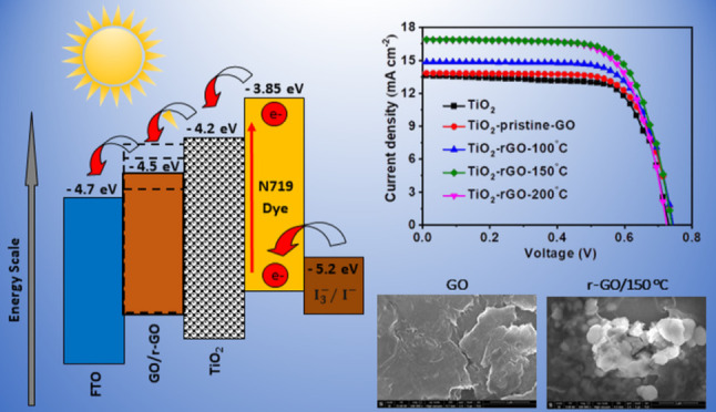
Graphene oxide (GO) nano-powder is synthesized by the modified Hummer’s method, and further thin films are deposited by using the water solution of GO through spin-coating. These films are thermally reduced along with the synthesized GO nano-powder at 50 to 200 °C in a high vacuum. Microstructural, electrical, and optical properties are expectedly controlled by thermal reduction. The electronic properties of GO are investigated by X-ray photoelectron spectroscopy and near-edge X-ray absorption fine structure. The reduction is confirmed by Raman spectroscopy. The work function and band gap of GO are tuned with the thermal reduction. The changes in properties of GO are not linear, and anomalous changes are observed for the reduction around 150 °C. Pristine and reduced GO nano-powder is incorporated into TiO2 paste to be the photoanode for dye-sensitized solar cells (DSSCs). It is observed that the performance of the fabricated cells is significantly enhanced for the GO reduced at 150 °C, and the cell exhibited a significant increment of ∼23% for the power conversion efficiency in comparison to DSSC based on an unmodified TiO2 photoanode.
1. Introduction
Solar energy is one of the favorite kinds of renewable energy, but its popularity is limited due to some extent by the high cost of conventional solar cells. Among different photovoltaics, dye-sensitized solar cells (DSSCs) have gained significant interest due to their light weight, remarkably high power conversion efficiency (PCE), overall low cost, and eco-friendly fabrication.1 The DSSCs consist of a transparent conducting oxide (TCO) layer; a wide band gap semiconductor as an electron acceptor, which is treated with an organic dye to harvest sunlight; a hole conductor medium, which is often iodide/tri-iodide electrolyte; and a platinum (Pt)-deposited counter electrode (CE).2 The sensitizer dye molecules absorb sunlight and get into an excited state. The excited dye molecule injects the electrons into the conduction band (CB) of the electron acceptor semiconductor material. It leads to the dye molecule being oxidized. The electrons are collected at the TCO layer and flow through the external circuit to the cathode CE side. These electrons combine with triiodide ions in the electrolyte, which help the oxidized dye molecules to return to the ground state by accepting electrons from iodide ions.3 Metal oxide wide band gap semiconductors such as ZnO and TiO2 are widely used for photogenerated electron acceptor layers because these can prevent shunting and leakage currents under reverse bias.1 The film of nanoparticles of mesoporous TiO2 has been identified as an excellent photoanode material due to its superior electrical and optical properties. It serves a dual purpose of providing a high surface area for the photovoltaic sensitizer as well as being a conductor of photogenerated electrons from the sensitizer.4 Although a mesoporous nanostructure provides a larger surface area for dye, the linkage between these nanoparticles must be improved so the photogenerated electrons can be collected at the cell anode instead of recombining with the oxidized dye molecules present in the TiO2 matrix.5 Furthermore, nanostructures of TiO2 also contain charge-trapping sites and larger grain boundaries, causing retardation in the charge transport.5 The incorporation of carbon nanostructures in the TiO2 matrix provides a solution that has been widely investigated recently to overcome the reasons for the inefficiency of DSSCs. These carbanion nanostructures improve the linkage between the TiO2 matrix, leading to faster electron transport, and/or reduce the recombination at the nanoparticle–electrolyte as well as nanoparticle–oxidized dye molecule interface.6 Graphene has been significantly explored for its applications in solar cells, such as transparent electrodes and CE in DSSCs. In addition to the transparent electrode and the CE, graphene also has been demonstrated as the electron acceptor and charge transfer medium to improve the efficiency of solar devices.7−9 Yang et al.9 added graphene as a 2D bridge into the nanocrystalline electrodes of DSSCs and found that the short-circuit current density (JSC) improved without losing the open-circuit voltage (VOC). The nanocrystalline TiO2 could anchor on the graphene flake trimly to form graphene bridges across several intermolecular forces, such as physisorption and electrostatic binding. Additionally, due to its excellent electrical conduction, the bridged graphene behaves as an electron transfer medium to quickly improve the electron transport from the CB of TiO2 at the anchor position, leading to the suppression of the recombination of photogenerated electrons.
The GO is a solution-processable hydrophilic allotrope of graphene. The GO is less conducting but offers several advantages over pristine graphene as being amenable to solution-based processes, making it easy to deposit as a thin film, with low-cost synthesis, ease of material processing, mechanical flexibility, adhesion compatibility with several substrates, and so forth. Furthermore, the high work function of GO creates a large energy level offset at the interface, leading to efficient charge separation.10 The typical structure of the fabricated DSSCs with a charge flow scheme is shown in Figure S1 (Supporting Information). In the DSSC structure, the mixing of GO flakes with TiO2 paste provides a better Brunauer–Emmet–Teller (BET) area and further improves charge transportation.11 The detailed photovoltaic parameters of the DSSC with GO, synthesized using different techniques as reported in the literature, are provided in Table S1 in the Supporting Information.
The reduction of GO led to be change in the CB energy level, and hence by controlling the reduction of GO, the electronic and optical properties of GO can be tuned in the desired way. Thermal annealing in the vacuum provides better control over reduction in comparison to chemical reduction processes.12−14
This paper reports on the studies of GO synthesized by the Hummers method and the nanostructures of reduced GO (rGO) achieved by thermal annealing of GO in the vacuum of ∼10–6 mbar at 50, 100, 150, and 200 °C. The GO is used in DSSCs to prove the enhancement in the device’s performance.
2. Experimental Section
2.1. Synthesis of GO Nano-Powder
The GO was prepared via the modified Hummers method.11,15 Fine mesh 2 g graphite powder (∼6 nm) was stirred with 2 g NaNO3 in 98% concentrated sulfuric acid (92 mL) for 1 h at 0 °C. Further, 12 g KMnO4 was gradually mixed in intervals, keeping the temperature below 10 °C, and the mixture was then stirred at 60 °C for 90 min. The final solution was diluted with 50 ml of water, which caused the heating of the solution to 90 °C. The reaction was terminated by adding 150 mL de-ionized (DI) water and 30% H2O2 solution (10 mL). This solution was filtered and washed using a 5% HCl aqueous solution. Finally, it was washed three times with DI water. The resulting GO powder was dried in a dark and cool place. The powder was slowly crushed into fine particles with the help of a mortar and pestle. Thus, the obtained powder was equally divided into five parts, and keeping the pristine one untouched, the other parts were reduced to 50, 100, 150, and 200 °C in high vacuum. All these powders were ready for further use to prepare the DSSC photoanode.
2.2. Deposition of GO and rGO Thin Films
The pristine GO powder was mixed ultra-sonically in the DI water for use for film deposition. Multi-layered films were deposited on the corning glass and fluorene-doped tin oxide (FTO) substrates by a spin coater at 2000 rpm. The deposited films were divided into equal pieces for further thermal reduction in high vacuum (∼10–6 mbar) at four different temperatures: 50, 100, 150, and 200 °C. All the thin films were characterized in detail to investigate the properties of GO and rGO and to establish the correlation with the DSSC performance.
2.3. Preparation of Photoanode
The photoanode was prepared by adding 5 wt % GO and rGO in TiO2 paste (18NR-T, Dyesol) by grinding method and then doctor blading for the desired thickness on FTO glass substrates (7 Ω/□). Fabrication of the DSSCs using N719 dye and iodine electrolyte has been reported in our earlier publication.16 TiO2 photoanodes were dipped in a 0.5 mM N719 dye (Dyesol) solution for ∼20 h at room temperature in the dark. Afterward, the photoanodes were washed with ethanol. Platinum CE was prepared using H2PtCl6 in ethanol.17 Subsequently, photoanode and platinum CE were sealed using 25 μm Surlyn. The iodine electrolyte was filled via predrilled holes in CE using the vacuum pump. The active area of the device was 0.25 cm2. Details of the characterization techniques are available in the Supporting Information.
2.4. Characterization Techniques
The GO and rGO samples are characterized via X-ray diffraction (XRD), Raman, X-ray photoelectron, near-edge X-ray absorption fine structure (NEXAFS), and UV–vis spectroscopy. Topography and morphology were investigated by scanning Kelvin probe microscopy (SKPM) and field emission scanning electron microscopy (FESEM). The detail of these characterization instruments is provided in the Supporting Information.
3. Results and Discussion
3.1. Reduction Tuning of Graphene Oxide
Figure 1 shows the XRD pattern of rGO films along with that of pristine GO films.
Figure 1.
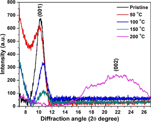
XRD pattern of pristine and rGO thin films.
The deposited films are in (001) orientation. A sharp and intense peak at 2θ = 10.211° with the (001) plane was observed with full width at half maxima (fwhm) 1.318° for the pristine sample; meanwhile, this peak was observed at 10.148, 10.631, and 10.742° with fwhm 1.327, 1.345, and 1.401° for the films reduced at 50, 100, and 150 °C, respectively. This peak was slightly shifted toward higher angles with the reduction temperature, which may decrease the interlayer spacing. Interlayer spacing in GO was possibly reduced due to the evaporation of oxygen links between the basal planes.18 However, it is observed that with the increment of reduction degrees, the peak gets weak and broad, and it indicates a change from a bigger flake structure to a micro-granular carbon matrix. However, the film reduced at 200 °C shows a broad peak around 22° (2θ) corresponding to (002) planes of the graphite framework.18,19 At such a higher degree of reduction, the deterioration of (001) meanwhile arising of the (002) illustrates the domination of graphite structure over graphene oxide (GO).
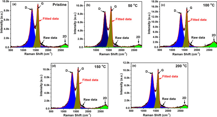
Figure 2 shows the Raman spectra of deposited GO and rGO thin films. Raman spectroscopy is a powerful tool to extract the identification of the GO samples, including the structural disorder defects, crystallization, and amount of carbon present during oxidation and reduction. The two major peaks at 1314 and 1591 cm–1, corresponding to the D-band and G-band, are observed clearly. Raman spectra of carbon-based materials are due to (i) the D-band being related to the disorder and defects in the hexagonal lattice and (ii) vibration mode for sp2 carbons atoms (G-band), which occurs owing to C–C stretching.20 The integrated intensity ID/IG ratio (calculated by dividing the area covered by the peaks, obtained from the origin peak fitting) slightly initially decreased from 1.89, calculated for the pristine sample, to 1.81, 1.78, and 1.75, with increase of the reduction temperature as 50, 100, and 150 °C, respectively. It indicates the removal of oxygen functionalities due to vacuum annealing and lesser defects on the surface of rGO.20 The ID/IG ratio significantly increased to 2.22 for the sample reduced at 200 °C. The increase in the ID/IG ratio is ascribed to an increase in the number and/or the size of sp2 clusters,21 and it may be due to the domination of the graphite matrix. A less-intense band was also observed in the Raman spectra at ∼2700 cm–1. This 2D band is the assertion of graphene structure and may provide information about the number of layers in GO sheets.21
Figure 2.
Raman spectra of GO thin films (a) pristine, and reduced at (b) 50, (c) 100 (d) 150, (e) 200 °C.
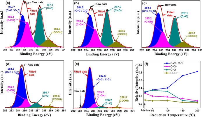
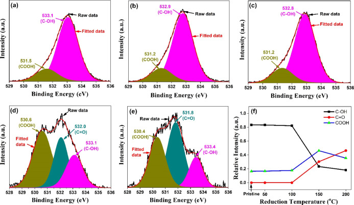
The atomic concentration and evolution of surface functionalization were determined by XPS. The full scan XPS survey analysis was carried out for atomic concentration, and high-resolution spectra of C1s and O1s were carried out for quantitative analysis of surface functionalities. The deconvolution of C1s and O1s spectra was performed using Casa XPS software with Shirley background correction. Figure 3 shows high-resolution C1s spectra. The deconvoluted peaks of the C1s spectrum of GO consist of four broad components. The component at 284.7 eV is attributed to the sp2 component (C=C/C–C). The component at 285.4 eV is attributed to hydroxyl configuration (C–OH). The components at 287.3 and 288.6 eV are assigned to carbonyl (>C=O) and carboxyl groups (COOH or OH–C=O). The high-resolution O1s are shown in Figure 4. The deconvoluted peaks of the O1s spectrum with binding energies (BE) 531.5, 532.0, and 533.1 eV represent −COOH (HO–C=O), >C=O, and C–OH, groups, respectively. The relative intensity of peak C–OH exhibits an initial increase at 50 °C (Table 1), which is most possibly due to the internal conversion of OH–C=O to C–OH.22 The shift of sp2 peak-maxima back to lower BE with increasing temperature signifies the transformation of electrically insulated GO to the conducting nature of graphite.
Figure 3.
Deconvoluted high-resolution C1s spectra for (a) pristine and the samples reduced at (b) 50, (c) 100 (d) 150, and (e) 200 °C; (f) reduction dependence of the relative contribution of C1s peak components.
Figure 4.
Deconvoluted high-resolution O1s spectra for (a) pristine and the samples reduced at (b) 50, (c) 100 (d) 150, (e) 200 °C; (f) reduction dependence of the relative contribution of O1s peak components.
Table 1. Reduction Dependence of the Relative Percentage Contribution of Different Functional Groups and the Relative Percentage Elemental Composition Estimated by Full Scan Spectra.
| group | pristine | 50 °C | 100 °C | 150 °C | 200 °C | |
|---|---|---|---|---|---|---|
| elemental composition (%) | C | 75.43 | 75.62 | 76.24 | 83.86 | 89.83 |
| O | 24.57 | 24.38 | 23.76 | 16.14 | 10.17 | |
| C=C/C–C | 30.05 | 36.43 | 40.72 | 71.53 | 83.16 | |
| C1S deconvolution | C–OH | 27.15 | 20.14 | 18.88 | 14.86 | 8.20 |
| >C=O | 35.33 | 32.74 | 31.65 | 9.32 | 5.11 | |
| –COOH | 10.05 | 8.75 | 8.09 | 4.29 | 3.54 | |
| O1S deconvolution | –COOH | 16.53 | 16.72 | 17.72 | 46.25 | 35.45 |
| >C=O | 30.38 | 46.39 | ||||
| C–OH | 83.47 | 83.28 | 82.28 | 23.36 | 18.16 |
The relative intensity of the sp2 component (C=C/C–C) increases as the reduction temperature increases, and an associated decrease of the oxygen groups (Table 1) confirms the reduction of GO as shown in Figures 3f and 4f, which agrees with the results demonstrated by Gaashani et al. and Bai et al.22,23
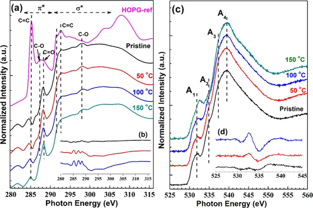
The NEXAFS spectra in the total electron yield (TEY) mode at the K-edge of principal constituents C and O are shown in Figure 5a,c, respectively. Meanwhile, the difference spectra are shown in the inset of these figures. The spectra were recorded at 90° incidence of the linear polarized X-ray beam. The NEXAFS measurement is an effective method for analyzing the unoccupied electronic structure of carbon-related materials. Furthermore, NEXAFS provides information about hetero generations in local structure, chemical bonding configurations, and nearest/next neighbor environment.
Figure 5.
Normalized NEXAFS for GO and rGO films: (a) C K-edge, (b) C K-edge difference spectra, (c) O K-edge, and (d) O K-edge difference spectra.
The resonance peaks for 1s−π* and 1s−σ* are located for the carbon K-edge NEXAFS observed around ∼285 and ∼293 eV, respectively. The spectral features for the carbon K-edge in the TEY mode are displayed in Table 2. The recorded spectra at the carbon K-edge are compared with standard spectra for highly ordered pyrolytic graphite (HOPG). The strong 2D geometry in the ideal structure of the graphite matrix is supposed to have strong directionality of the orbitals: hence, r-orbitals lie within the basal plane, and p-orbitals are directed perpendicular to the basal plane. For the sp2 hybridized carbon structure, the sigma bond lies in the plane of the structure, and the pi-bond exists out of the plane (in the perpendicular basal plane), so the E- vector of X-rays must be parallel for perpendicular incidence to the highly ordered graphene structure. As a result, the intensity of the 1s−π* transition should be extremely poor compared to 1s−σ*. However, the observed intensity of π* in recorded spectra compared to HOPG suggests that the synthesized GO and rGO do not possess a perfectly plane structure. It may be due to the coexistence of different micro-domains and disordered stacking of GO and rGO planes contrasted to HOPG and the disorder induced by the oxidation processes. Moreover, the hydroxyl and epoxy groups dispersed randomly on the top and bottom of the basal plane of each graphene coating would draw the bonded carbon atoms up and down concerning the basal plane. The 1s−σ* transition observed with a broad peak compared to HOPG also implies a defective sp2 geometry.
Table 2. Spectral Features for the Carbon K-Edge in the TEY Mode.
| photon energy (eV) | NEXAFS spectral feature |
|---|---|
| 285.2 | excitation of carbon in the sp2 network into the π* bond |
| 286.5 | π* excitation for carbon that is single bonded to oxygen either in hydroxyl or in epoxy configuration/functional groups |
| 288.7 | C=O, a π* resonance in carboxyl groups |
| 291.6 | σ resonance is broader, and absence of core excitation defects, the sp2 network |
| 292.6 | σ* resonance for un-interruptedsp2 network |
| 297.5 | σ* resonance attribute to single-bonded oxygen |
| 330 | strong functionalization and interference with many states, C=O sigma features from carboxyl expected cannot be resolved (usually not shown in spectra) |
The transition observed at 288.7 eV related to π* resonance in the carboxyl group (>C=O, shown by the arrow in Figure 5a), is intensified with reduction temperature; this relative change can be observed from the difference spectra shown in the inset of Figure 5b and result in the gradual reduction of GO. A shoulder peak of ∼292 eV of rGO should be an excitonic state; the presence of this excitonic state implies that rGO consists of too many sp2 hybridized carbon atoms, as this peak is commonly observed for pristine graphite.24
The XAS spectra for the K edge of O1S are recorded with two clear resonance peaks at ∼532 and ∼540 eV (Figure 5c). The peak around 532 eV could be assigned to π* resonances, and the peak around 540 eV is possible from σ* resonances of the carbonyl group (−C=O).24,25 Spectral features of the O–K edge (A1, A2, A3, and A4) are shown in Table 3. The intensities of both transitions are notably affected by the reduction temperature, as can be seen clearly from the difference spectra (Figure 5d), and it leads to the tunable defunctionalization of GO. NEXAFS spectra suggested relatively higher degrees of recoveries of π-conjugation upon reduction.
Table 3. Spectral Features for the Oxygen K-Edge in the TEY Mode.
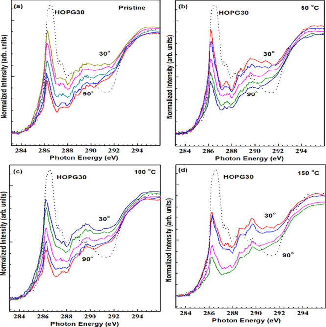
The angle dependence NEXFAS spectra recorded in the PEF mode are shown in Figure 6. It can be observed from the spectra that synthesized samples are isotropic.
Figure 6.
Angle dependence of the GO samples in the PEY mode (a) pristine, and reduced at (b) 50, (c) 100, and (d) 150 °C.
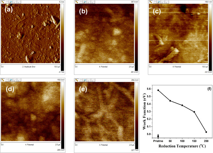
Figure 7a–e shows the Kelvin probe microscope spectra of pristine GO and rGO thin films thermally reduced at 50, 100, 150, and 200 °C, respectively. SKPM is a modified version of atomic force microscopy, which provides non-destructive and non-contact topography of the sample, including the contact potential difference between a sample and the tip. The SKPM is employed to determine the work function of these films. For this purpose, one set of films was deposited on FTO-coated glass substrates and annealed along with other samples. It provides desired measurement results without introducing extra effects due to Schottky barrier formation.29,30 It is well known that the work function depends on the carrier concentrations. Hence, tuning GO from semiconductor to metallic work function will have an expected response. Scanning probe methods such as SKPM provide spatial resolution and allow the detection of local surface potentials.30 In general, Vkelvin is the voltage needed to compensate for the non-biased setup (Vbias = 0), and Vkelvin is equal to the contact potential difference between the tip and the sample.31
where Φtip and Φsample are the work functions of the tip and sample, respectively, and e is the elementary charge. This method is implied to investigate the surface potential of GO thin films on FTO-coated glass substrates.
Figure 7.
SKPM images of GO and rGO thin films (a) pristine, (b) 50, (c) 100, (d) 150, (e) 200 °C, and (f) work function calculated from Kelvin probe microscope spectra.
During the measurements of surface potential scans, Gaussian distribution is considered due to typical disorder in a polycrystalline carbonaceous semiconductor thin film.32 The work function is measured at around 5.58 eV for the pristine GO; meanwhile, it is decreased with a reduction grade of GO (shown in Figure 7f), with the values 5.44, 5.38, 5.29, and 5.03 eV for the samples reduced at 50, 100, 150, and 200 °C, respectively. The reduction in the work function may be a possible reason to enhance the charge transport property of GO.
The UV–vis absorption spectrum of aqueous GO dispersion
is shown in Figure S2 (Supporting Information). The pristine GO shows two kinds of characteristic features: a
major peak is observed at ∼235 nm due to π–π*
transitions of aromatic ring electrons related to C=C and C–C
bonds. Another characteristic shoulder peak at ∼307 nm corresponds
to the n−π* transitions of the carbonyl group (C=O)
electrons.33 The band gap is evaluated
by employing Tauc plots (shown in the inset of Figure S2) for the spectra to fit the data, assuming  relationship corresponding to the indirect
transitions, where “α” is the absorption coefficient
and “hν” is photon energy.34 The sharp adsorption edges were not observed
in the Tauc plots due to the domination of the less-arranged carbon
matrix and non-uniform oxidation levels in GO itself. The band gap
is measured at around 2.76 eV for the pristine one, which is inconsistent
with the reported indirect band gap for GO.34,35 Meanwhile, the band gap shrinkage is significant with values of
2.35, 2.12, 1.24, and 0.79 eV for the samples reduced at 50, 100,
150, and 200 °C, respectively.
The surface morphology of pristine GO and rGO films (thermally reduced at 50, 100, 150, and 200 °C) analyzed by FESEM is shown in Figure S3a–e (Supporting Information). The reduction process can reduce as well as exfoliate the pristine GO into fluffy and wrinkled rGO, which can be observed. The deformation of rGO observed in FESEM images is mostly due to the elimination of oxygen-containing groups from the carbon planes during the reduction. The wrinkled structure offers a maximum accessible surface area of rGO to occupy the charge carriers from TiO2. The samples were reduced at 150 °C, and higher temperatures were noticed with tiny-granular morphology instead of flakes as was observed in the pristine one. The granular microstructure enhances the surface-to-volume ratio and further assists in improving the charge transfer. The absence of charging during SEM imaging suggests the relative electrically conductive behavior of rGO, which is related to the electron charge transport property of rGO.36
3.2. Photovoltaic Performance
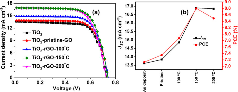
The current density–voltage (J–V) curve of DSSCs using GO and rGO are shown in Figure 8a, with Table 4 giving detailed parameters. The JSC of DSSCs using TiO2 photoanode is 13.6 mA cm–2, with a PCE of 7.13%. After the addition of pristine GO into the TiO2 photoanode, there is a slight enhancement in JSC, with a PCE of 7.35%. rGO-based TiO2 photoanodes yield further enhancement in JSC and PCE, with the values being dependent on reduction treatment temperature as explained below.
Figure 8.
(a) J–V curve of DSSCs using GO/rGO photoanodes and (b) JSC and PCE of DSSC with reduction temperature.
Table 4. Photovoltaic Parameters of DSSCs.
| DSSC | JSC (mA cm–2) | VOC (mV) | FF (%) | PCE (%) |
|---|---|---|---|---|
| TiO2 | 13.61 | 731 | 71.7 | 7.13 ± 0.09 |
| TiO2-pristine GO | 13.84 | 743 | 71.5 | 7.35 ± 0.10 |
| TiO2-rGO-100 °C | 14.85 | 743 | 71.4 | 7.87 ± 0.09 |
| TiO2-rGO-150 °C | 16.90 | 739 | 70.5 | 8.80 ± 0.08 |
| TiO2-rGO-200 °C | 16.85 | 725 | 69.5 | 8.49 ± 0.10 |
The DSSCs with TiO2-rGO-150 °C exhibited the highest JSC of 16.90 mA cm–2 and the highest PCE of 8.80% compared to as-deposited DSSC. The addition of GO/r-GO into the TiO2 photoanode improves the charge transport and acts as a pathway for charge transfer.21,37 The reduction of GO at the appropriate level as here for 150 °C may be the key reason to adjust the energy level of GO CB energy that implies a higher driven force to push the electron from TiO2 to improve the charge transfer. DSSCs with the composite photoanode (TiO2-rGO-150 °C) also effectively suppress the charge recombination and the back reaction of the photoelectron, which diminishes the diffuse barrier to photoelectron transfer and improves the overall improved performance of the DSSC. The optimum level of oxygen, optical properties, and microstructure seems to occur for improving the performance of DSSCs with rGO-150 °C. The performance of DSSCs with rGO-200 °C decreases due to changes in the phase formation of rGO taking place. There is a slight change in the VOC of rGO-150 °C and rGO-200 °C, and it is due to the change in the work function. Figure 8b shows the change in JSC and PCE with respect to the reduction temperature of GO. JSC of DSSCs increases to 150 °C reduction temperature compared to as-deposited DSSCs. JSC starts decreasing at 200 °C due to changes in the microstructure and graphite-like phase formation (as discussed in the earlier section).
4. Conclusions
Modified Hummers method was employed for the synthesis of GO. Thin films coated on corning glass substrates as well as synthesized GO powder were gradually reduced by the vacuum annealing process at four different temperatures (50, 100, 150, and 200 °C). It is observed that the pristine structure turned from a semiconductor to a graphite matrix with the reduction, and it significantly affects the optical, microstructural, and electronic structure and hence the charge transfer properties of GO. It is found that there are anomalous changes in the properties of GO with a reduction of around 150 °C. At lower degrees of reduction (pristine level), the GO layers with a fluffy microstructure and poor charge transfer. On the other hand, at a very high reduction (200 °C), a graphite-like layer is created. With the selection of an appropriate reduction treatment, the maximum advantages can be granted to the GO properties. The DSSCs fabricated with an optimized photoanode having a mesoporous TiO2 mixed with GO nanostructures reduced at 150 °C show the best performance with a JSC of 16.90 mA cm–2, VOC of 739 mV, and FF of 70.5%, with a PCE of 8.80%. Therefore, the incorporation of rGO reduced at the optimum level can play an essential role in improving the DSSC performance.
Acknowledgments
Dr. Amanpal Singh wants to thank the Indian Institute of Technology, Mandi (Himachal Pradesh, India), for the institution’s post-doctoral fellowship during the partial work, and Dr. Suman K. Pal for his support. The authors are thankful to Prof. J.M. Chen (BL20A1), National Synchrotron Radiation Center (NSRRC), Hsinchu, Taiwan, for supporting NEXAFS measurements and Materials Research Centre, MNIT, Jaipur, for XPS characterization facilities.
Supporting Information Available
The Supporting Information is available free of charge at https://pubs.acs.org/doi/10.1021/acsomega.2c05637.
Various characterization instruments, comparative detail of photovoltaic parameters of DSSCs with GO synthesized using different techniques as reported in the literature, schematic of the charge flow in DSSCs, absorption spectra of aqueous GO dispersion with Tauc plots for the deposited GO and rGO thin films, and FESEM images of GO and rGO films (PDF)
The authors declare no competing financial interest.
Supplementary Material
References
- Wang J. T. W.; Ball J. M.; Barea E. M.; Abate A.; Alexander-Webber J. A.; Huang J.; Saliba M.; Mora-Sero I.; Bisquert J.; Snaith H. J.; Nicholas R. J. Low-Temperature Processed Electron Collection Layers of Graphene/TiO2 Nanocomposites in Thin Film Perovskite Solar Cells. Nano Lett. 2014, 14, 724–730. 10.1021/NL403997A/SUPPL_FILE/NL403997A_SI_001.PDF. [DOI] [PubMed] [Google Scholar]
- Kokkonen M.; Talebi P.; Zhou J.; Asgari S.; Soomro S. A.; Elsehrawy F.; Halme J.; Ahmad S.; Hagfeldt A.; Hashmi S. G. Advanced Research Trends in Dye-Sensitized Solar Cells. J. Mater. Chem. A 2021, 9, 10527–10545. 10.1039/D1TA00690H. [DOI] [PMC free article] [PubMed] [Google Scholar]
- Dong P.; Zhu Y.; Zhang J.; Peng C.; Yan Z.; Li L.; Peng Z.; Ruan G.; Xiao W.; Lin H.; Tour J. M.; Lou J. Graphene on Metal Grids as the Transparent Conductive Material for Dye Sensitized Solar Cell. J. Phys. Chem. C 2014, 118, 25863–25868. 10.1021/JP505735J/SUPPL_FILE/JP505735J_SI_001.PDF. [DOI] [Google Scholar]
- Ziaeifar F.; Alizadeh A.; Shariatinia Z. Dye Sensitized Solar Cells Fabricated Based on Nanocomposite Photoanodes of TiO2 and AlMo0.5O3 Perovskite Nanoparticles. Sol. Energy 2021, 218, 435–444. 10.1016/J.SOLENER.2021.03.024. [DOI] [Google Scholar]
- Wei L.; Chen S.; Yang Y.; Dong Y.; Song W.; Fan R. Reduced Graphene Oxide Modified TiO2 Semiconductor Materials for Dye-Sensitized Solar Cells. RSC Adv. 2016, 6, 100866–100875. 10.1039/C6RA22112B. [DOI] [Google Scholar]
- Bell N. J.; Du A.; Ng Y. H.; Coster H.; Smith S. C.; Amal R. Understanding the Enhancement in Photoelectrochemical Properties of Photocatalytically Prepared TiO2-Reduced Graphene Oxide Composite. J. Phys. Chem. C 2011, 115, 6004–6009. 10.1021/jp1113575. [DOI] [Google Scholar]
- Muchuweni E.; Martincigh B. S.; Nyamori V. O. Recent Advances in Graphene-Based Materials for Dye-Sensitized Solar Cell Fabrication. RSC Adv. 2020, 10, 44453–44469. 10.1039/D0RA08851J. [DOI] [PMC free article] [PubMed] [Google Scholar]
- Roy-Mayhew J. D.; Aksay I. A. Graphene Materials and Their Use in Dye-Sensitized Solar Cells. Chem. Rev. 2014, 114, 6323–6348. 10.1021/cr400412a. [DOI] [PubMed] [Google Scholar]
- Yang N.; Zhai J.; Wang D.; Chen Y.; Jiang L. Two-Dimensional Graphene Bridges Enhanced Photoinduced Charge Transport in Dye-Sensitized Solar Cells. ACS Nano 2010, 4, 887–894. 10.1021/nn901660v. [DOI] [PubMed] [Google Scholar]
- Min S.; Lu G. Dye-Sensitized Reduced Graphene Oxide Photocatalysts for Highly Efficient Visible-Light-Driven Water Reduction. J. Phys. Chem. C 2011, 115, 13938–13945. 10.1021/jp203750z. [DOI] [Google Scholar]
- Jo J.; Lee S.; Gim J.; Song J.; Kim S.; Mathew V.; Alfaruqi M. H.; Kim S.; Lim J.; Kim J. Facile Synthesis of Reduced Graphene Oxide by Modified Hummer’s Method as Anode Material for Li-, Na- and K-Ion Secondary Batteries. R. Soc. Open Sci. 2019, 6, 181978. 10.1098/RSOS.181978. [DOI] [PMC free article] [PubMed] [Google Scholar]
- Toe M. Z.; Pung S. Y.; Yaacob K. A.; Matsuda A.; Tan W. K.; Han S. S. Effect of TiO2 Sol on the Conversion Efficiency of TiO2 Based Dye-Sensitized Solar Cell. J. Sol. Gel Sci. Technol. 2020, 95, 439–446. 10.1007/S10971-020-05325-9. [DOI] [Google Scholar]
- Sengupta I.; Chakraborty S.; Talukdar M.; Pal S. K.; Chakraborty S. Thermal Reduction of Graphene Oxide: How Temperature Influences Purity. J. Mater. Res. 2018, 33, 4113–4122. 10.1557/JMR.2018.338. [DOI] [Google Scholar]
- Emiru T. F.; Ayele D. W. Controlled Synthesis, Characterization and Reduction of Graphene Oxide: A Convenient Method for Large Scale Production. Egypt. J. Basic Appl. Sci. 2017, 4, 74–79. 10.1016/J.EJBAS.2016.11.002. [DOI] [Google Scholar]
- Nathabumroong S.; Poochai C.; Chanlek N.; Eknapakul T.; Sonsupap S.; Tuichai W.; Sriprachuabwong C.; Rujirawat S.; Songsiriritthigul P.; Tuantranont A.; Yimnirun R. Enhanced Surface and Electrochemical Properties of Nitrogen-Doped Reduced Graphene Oxide by Violet Laser Treatment for High Charge Storage and Lower Self-Discharge Supercapacitors. J. Power Sources 2021, 513, 230517. 10.1016/J.JPOWSOUR.2021.230517. [DOI] [Google Scholar]
- Swami S. K.; Chaturvedi N.; Kumar A.; Dutta V. Dye Sensitized Solar Cells Using the Electric Field Assisted Spray Deposited Kesterite (Cu2ZnSnS4) Films as the Counter Electrodes for Improved Performance. Electrochim. Acta 2018, 263, 26–33. 10.1016/J.ELECTACTA.2018.01.030. [DOI] [Google Scholar]
- Swami S. K.; Chaturvedi N.; Kumar A.; Dutta V. Effect of Zinc Precursor on Cu2ZnSnS4 Nanoparticles Synthesized by the Solvothermal Method and Its Application in Dye-Sensitized Solar Cells as the Counter Electrode. Mater. Today Energy 2018, 9, 377–382. 10.1016/J.MTENER.2018.06.008. [DOI] [Google Scholar]
- Jeong H.-K.; Lee Y. P.; Lahaye R. J. W. E.; An K.-H.; Kim I. J.; Yang C. W.; Park C.-Y.; Park M.-H.; Ruoff R. S.; Lee Y. H. Evidence of Graphitic AB Stacking Order of Graphite Oxides. J. Am. Chem. Soc. 2008, 130, 1362–1366. 10.1021/ja076473o. [DOI] [PubMed] [Google Scholar]
- Li Z. Q.; Lu C. J.; Xia Z. P.; Zhou Y.; Luo Z. X-Ray Diffraction Patterns of Graphite and Turbostratic Carbon. Carbon 2007, 45, 1686–1695. 10.1016/J.CARBON.2007.03.038. [DOI] [Google Scholar]
- Mondal J.; Srivastava S. δ-MnO2 Nanoflowers and Their Reduced Graphene Oxide Nanocomposites for Electromagnetic Interference Shielding. ACS Appl. Nano Mater. 2020, 3, 11048–11059. 10.1021/acsanm.0c02247. [DOI] [Google Scholar]
- Cheng G.; Akhtar M. S.; Yang O.-B.; Stadler F. J. Novel Preparation of Anatase TiO2@Reduced Graphene Oxide Hybrids for High-Performance Dye-Sensitized Solar Cells. ACS Appl. Mater. Interfaces 2013, 5, 6635–6642. 10.1021/am4013374. [DOI] [PubMed] [Google Scholar]
- Al-Gaashani R.; Najjar A.; Zakaria Y.; Mansour S.; Atieh M. A. XPS and Structural Studies of High Quality Graphene Oxide and Reduced Graphene Oxide Prepared by Different Chemical Oxidation Methods. Ceram. Int. 2019, 45, 14439–14448. 10.1016/J.CERAMINT.2019.04.165. [DOI] [Google Scholar]
- Bai L.; Xu Y.; Liu A.; Dong L.; Zhang K.; Li W. S.; Zhao F. G. Unusual Graphite Fluoride Hydrolysis toward Unconventional Graphene Oxide for High-Performance Supercapacitors and Li-Ion Batteries. Chem. Eng. J. 2022, 434, 134639. 10.1016/J.CEJ.2022.134639. [DOI] [Google Scholar]
- Yadav A. K.; Padma N.; Ghorai G.; Sahoo P. K.; Rao R.; Banarjee S.; Rajarajan A. K.; Kumar P.; Jha S. N.; Bhattacharyya D. Local Structural Investigations of Graphitic ZnO and Reduced Graphene Oxide Composite. Appl. Surf. Sci. 2021, 565, 150548. 10.1016/J.APSUSC.2021.150548. [DOI] [Google Scholar]
- Lee V.; Dennis R. v.; Jaye C.; Wang X.; Fischer D. A.; Cartwright A. N.; Banerjee S. In Situ Near-Edge x-Ray Absorption Fine Structure Spectroscopy Investigation of the Thermal Defunctionalization of Graphene Oxide. J. Vac. Sci. Technol., B 2012, 30, 061206. 10.1116/1.4766325. [DOI] [Google Scholar]
- Outka D. A.; Stöhr J.; Madix R. J.; Rotermund H. H.; Hermsmeier B.; Solomon J. NEXAFS Studies of Complex Alcohols and Carboxylic Acids on the Si(111)(7×7) Surface. Surf. Sci. 1987, 185, 53–74. 10.1016/S0039-6028(87)80613-1. [DOI] [Google Scholar]
- Gandhiraman R. P.; Javier C.; Koehne J. E.; Chen B.; Nordlund D.; Meyyappan M. X-ray Absorption Study of Graphene Oxide and Transition Metal Oxide Nanocomposites. J. Phys. Chem. C 2014, 118, 18706–18712. 10.1021/jp503941t. [DOI] [PMC free article] [PubMed] [Google Scholar]
- Pacilé D.; Meyer J. C.; Fraile Rodríguez A.; Papagno M.; Gómez-Navarro C.; Sundaram R. S.; Burghard M.; Kern K.; Carbone C.; Kaiser U. Electronic Properties and Atomic Structure of Graphene Oxide Membranes. Carbon 2011, 49, 966–972. 10.1016/J.CARBON.2010.09.063. [DOI] [Google Scholar]
- Ramamoorthy H.; Buapan K.; Chiawchan T.; Thamkrongart K.; Somphonsane R. Exploration of the Temperature-Dependent Correlations Present in the Structural, Morphological and Electrical Properties of Thermally Reduced Free-Standing Graphene Oxide Papers. J. Mater. Sci. 2021, 56, 15134–15150. 10.1007/S10853-021-06262-W/FIGURES/7. [DOI] [Google Scholar]
- Maragliano C.; Lilliu S.; Dahlem M. S.; Chiesa M.; Souier T.; Stefancich M. Quantifying Charge Carrier Concentration in ZnO Thin Films by Scanning Kelvin Probe Microscopy. Sci. Rep. 2014, 4, 1–7. 10.1038/srep04203. [DOI] [PMC free article] [PubMed] [Google Scholar]
- Druga T.; Wenderoth M.; Lüpke F.; Ulbrich R. G. Graphene-Metal Contact Resistivity on Semi-Insulating 6H-SiC(0001) Measured with Kelvin Probe Force Microscopy. Appl. Phys. Lett. 2013, 103, 051601. 10.1063/1.4816955. [DOI] [Google Scholar]
- Bässler H. Charge Transport in Disordered Organic Photoconductors a Monte Carlo Simulation Study. Phys. Status Solidi B 1993, 175, 15–56. 10.1002/PSSB.2221750102. [DOI] [Google Scholar]
- Liu W.; Speranza G. Tuning the Oxygen Content of Reduced Graphene Oxide and Effects on Its Properties. ACS Omega 2021, 6, 6195–6205. 10.1021/acsomega.0c05578. [DOI] [PMC free article] [PubMed] [Google Scholar]
- Méndez-Romero U. A.; Pérez-García S. A.; Xu X.; Wang E.; Licea-Jiménez L. Functionalized Reduced Graphene Oxide with Tunable Band Gap and Good Solubility in Organic Solvents. Carbon 2019, 146, 491–502. 10.1016/J.CARBON.2019.02.023. [DOI] [Google Scholar]
- Hunt A.; Kurmaev E. Z.; Moewes A. Band Gap Engineering of Graphene Oxide by Chemical Modification. Carbon 2014, 75, 366–371. 10.1016/J.CARBON.2014.04.015. [DOI] [Google Scholar]
- Strankowski M.; Piszczyk Ł.; Kosmela P.; Korzeniewski P. Morphology and the Physical and Thermal Properties of Thermoplastic Polyurethane Reinforced with Thermally Reduced Graphene Oxide. Pol. J. Chem. Technol. 2015, 17, 88–94. 10.1515/PJCT-2015-0073. [DOI] [Google Scholar]
- Peiris D. S. U.; Ekanayake P.; Karunaratne B. A.; Petra M. I. Improved Performance of DSSC Photoanodes After the Modification of TiO2 with Reduced Graphene Oxide. J. Electron. Mater. 2021, 50, 1044–1053. 10.1007/S11664-020-08642-5. [DOI] [Google Scholar]
Associated Data
This section collects any data citations, data availability statements, or supplementary materials included in this article.


