Abstract
Antimony (Sb) chalcogenides such as antimony selenide (Sb2Se3) and antimony sulfide (Sb2S3) have distinct properties to be used as absorber semiconductors for harnessing solar energy including high absorption coefficient, tunable bandgap, low toxicity, phase stability. The potentiality of Sb2Se3 and Sb2S3 as absorber material in Al/FTO/Sb2Se3(or Sb2S3)/Au heterojunction solar cells (HJSCs) with 2D tungsten disulfide (WS2) electron transport layer (ETL) layer has been investigated numerically using SCAPS-1D solar simulator. A systematic investigation of the impact of physical properties of each active material of Sb2Se3, Sb2S3, and WS2 on photovoltaic parameters including layer thickness, carrier doping concentration, bulk defect density, interface defect density, carrier generation, and recombination. This study emphasizes the exploration of causes of low performance of actual devices and demonstrates the individual variation in the open-circuit voltage (VOC), short-circuit current density (JSC), fill factor (FF), power conversion efficiency (PCE) and quantum efficiency (QE). Thereby, highly potential heterostructures of Al/FTO/WS2/absorber (Sb2Se3 or Sb2S3)/Au proposed, in which, the PCE over 28.20 and 26.60% obtained with VOC of 850 and 1230 mV, Jsc of 38.0 and 24.0 mA/cm2, and FF of 86.0 and 89.0% for Sb2Se3 and Sb2S3 absorber, respectively. These detailed findings revealed that the Sb-chalcogenide heterostructure with potential WS2 ETL can be used to realize the fabrication of feasible thin film solar cells and thus the design of high-efficiency high-current (HEHC) and high-efficiency high-voltage (HEHV) solar panels.
Keywords: Heterojunction solar cell, Sb2Se3, Sb2S3, WS2 electron transport layer, SCAPS-1D
Graphical abstract
Highlights
-
•
Antimony chalcogenide (Sb2Se3 and Sb2Se3)-based TFSCs with WS2 electron transport layer were studied by SCAPS-1D simulator.
-
•
Systematic investigation on the impacts of thickness, doping, bulk, and interface defect densities on the PV performance.
-
•
PCE of 28.20% (26.60%) was found in a 1280 nm thick n+/n/p junction Sb2Se3 (Sb2S3) solar cell under adjusted condition.
-
•
The simulation was verified with the Shockley–Queisser (SQ) limit including experimental as well as simulation works.
Heterojunction solar cell; Sb2Se3; Sb2S3; WS2 electron transport layer; SCAPS-1D.
1. Introduction
Photovoltaic technologies provide a clean, eco-friendly, cost-effective, and long-term solution to meet rising worldwide energy demand by directly converting solar energy into electricity [[1], [2], [3], [4], [5]]. Different types of solar cells have been technologically advanced to meet increasing energy demands [[6], [7], [8], [9]], including silicon (Si) [[10], [11], [12], [13], [14], [15]], cadmium telluride (CdTe), copper indium gallium selenide (CIGS), copper zinc tin sulfide (CZTS), polymer, inorganic metal chalcogenide, dye-sensitized solar cell (DSSC) [[16], [17], [18]], quantum dot (QD), and perovskite-based solar cells [[19], [20], [21], [22]].
A single-junction solar cell with a bandgap of around 1.14 eV of the absorber layer can provide the highest power conversion efficiency (PCE) of 33.3%, according to the Shockley-Queisser (SQ) model [23]. Thin-film solar cells (TFSCs) based on silicon, CIGS, and CdTe, on the other hand, have attained PCEs of over 20% [6,24,25]. Despite the abundance of Si on earth, the rarity of In, Ga, and Te, as well as the toxicity of Cd, limit their use on a broad scale, which has been one of the key challenges for CIGS and CdTe solar cells [26,27]. As a result, in the last decade, various novel earth-abundant absorber materials, such as Cu2SnS3 [28], Cu2GeS3 [29], Cu2(Sn,Ge)S3 [30], GeSe [31], CuSbS2 [32], CuSbSe2 [33], Cu2ZnSnSe4 [34], FeS2 [35], FeSi2 [36], SnSe [37], Sb2Se3 [38], and Sb2S3 [39], have been suggested as an alternative for the eco-friendly, and golden triangle requirements: low cost, high PCE, and long-term durability of TFSCs [1].
Among them, Sb2Se3 and Sb2S3 have attracted considerably and advanced hurriedly [[39], [40], [41], [42], [43], [44]] due to their excellent photovoltaic properties, such as a suitable bandgap (1.1–1.7 eV) for single-junction solar cells [45], a high absorption coefficient (>105 cm−1 at visible light) [46], a low melting point (550 °C) [47], low-cost constituents [48], and low structural complexity with only one crystallographic phase [49].
To fabricate Sb2Se solar cells, several major approaches [40,48,50] with different buffer layers [40,51,52] have been used. It's worth noting that while Sb2Se has been investigated for more than 40 years, its usage as absorber material in solar cells has only recently become popular, with significant progress occurring since 2009. A comparative study of experimentally fabricated Sb2Se3-and Sb2S3-based heterojunction solar cells (HJSCs) are summarized in Tables S1 and S2 in the supplementary materials. Overall, the first experimental efficiency of the Sb2Se3 and Sb2S3 TFSC in 2009 was 0.66% [53] and 3.7% [54] which improved to 9.2% in 2019 [55] and 6.53% in 2020 [56], respectively. Lin et al. fabricated glass/Mo/Sb2Se3/CdS/ITO/Ag solar cells using the sputtering technique and delivered PCE of 7.43% [57]. In recent times, Tang et al. have achieved PCE 8.64% by sputtering technique with record VOC of 0.52 V [58].
However, using the SCAPS-1D simulator, multiple Sb2Se [[59], [60], [61]] and Sb2Se3 [62] based solar cell architectures with varying electron transport layers (ETLs) [63,64] and hole transport layers (HTLs) [65,66] have recently been explored, with reasonably good photovoltaic (PV) performance. Basak et al. have recently explored the Sb2S3 (or Sb2Se3)/CdS heterojunction solar cell (HJSC) in SCAPS-1D and found PCEs of 9.51% and 12.62%, respectively, for Sb2S3 and Sb2Se3 HJSC [67]. However, according to the review of simulation-based studies on these solar cells, the maximum efficiency is 23.18% [65]. Yet their theoretical PCE is inferior to that of comparable commercial TFSCs [24,68]. Furthermore, while CdS is widely used as a window or buffer layer in PV devices due to its appropriate bandgap [69], the toxicity of Cd [70] leads researchers to continue looking for other environmentally friendly and wide bandgap materials to use as window or buffer layer in antimony (Sb) chalcogenide-based solar cells [70]. In this perspective, tungsten disulfide (WS2) offers relaxed carrier transport by acceptable band alignment with Sb2Se3 and Sb2S3-based solar cells, while also being earth-abundant, economical, adhesive, and non-toxic [70]. Consequently, performing systematic numerical analysis in the SCAPS-1D simulator, we have designed, simulated, and proposed simplified designs for the efficiency enhancement of Sb2Se3 and Sb2S3-based solar cells employing WS2 as ETL. Our proposed devices, with their optimized parameters, provide superior results to the devices proposed earlier [[65], [66], [67]].
2. Modeling and simulation
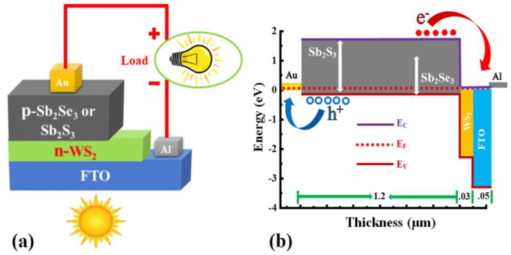
Figure 1 shows the schematic structure and band alignment of proposed Al/FTO/WS2/Sb2Se3 (or Sb2S3)/Au HJSC structure, where FTO, WS2, and Sb2Se3 (or Sb2S3) are used as the n+-type window layer, n-type electron transport, or buffer layer, and the p-type active absorber layer, respectively.
Figure 1.
(a) Proposed Al/FTO/WS2/Sb2Se3(or Sb2S3)/Au HJSC, and (b) corresponding band diagram.
In this work, a one-dimensional solar cell capacitance simulator (SCAPS-1D) of version 3.3.07 [71,72] has been used to conduct the whole investigation. Though the SCAPS simulator allows researchers to explore devices with up to seven layers [69], the current structure of the designed solar cell with only three layers has a substantial impact on PV performance, as will be described in subsequent section 3. Light travels through the FTO-coated glass substrate and WS2 ETL and finally reaches the absorber layer in this approach. FTO is a common material for substrate in HJSCs due to its chemical and mechanical durability, thermal stability, low toxicity, and inexpensive raw material and processing costs [73,74] which is why we used this substrate to achieve a higher value for the design cell's performance to cost ratio. However, considering the practical constraints we assumed 90% transmission (visible absorption of FTO is 0.04) of light incident onto the surface of the FTO layer [69].
Since, Au is a noble metal having two major advantages: (a) chemically inert and (b) high work function metal (5.1–5.3 eV), which is required for hole extraction efficiently at the back interface in p-type absorbers (VBM of 5.36 eV) forming ohmic contact, Au was chosen as back metal contact. J. Zhang et al reported that the forward current in Sb2Se3 solar cells with Al(WF of 4.0–4.2 eV) back contact is very low even under large forward bias (0.2 mA/cm2 at 1 V, owing to a large barrier at the back interface for hole extraction and consequently blocking current across the solar cell significantly [75]. Although they proposed NiOx/Ni as a promising one alike Au as back contact, Au was preferred to investigate the efficacy of the absorber and ETL layer in detail with no use of HTL or any HTL like NiOx as recommended. On the other hand, Al (WF of 4.0–4.2 eV) was used as a front metal electrode with FTO (4.0 eV) considering both the work function for obtaining ohmic contact and its availability. Since, Aluminum is the most abundant metal on Earth, as well as one of the cheapest metals, therefore, Al was chosen as the front metal contact with FTO TCO.
Nevertheless, SCAPS-1D software was developed based on the semiconductor principal equations and is largely used to model semiconductor solar cells [71]. More particularly, the Poisson, hole, and electron continuity equations are employed to determine the numerical assessments of the modeled solar cell structure, as shown in Eqs. (1), (2), and (3), respectively [65,76].
| (1) |
| (2) |
| (3) |
where, Ψ, q, ε, NA (ND), and ρp (ρn) denote electrostatic potential, the charge of an electron, dielectric permeability, hole (electron) concentration, and hole (electron) distribution, respectively. In addition, JP (Jn), GOP, R, and p (n) present current density contributed by hole (electron), optical carrier generation rate, recombination rate, and free acceptor (donor) concentration, respectively.
The drift-diffusion formulas of Eqs. (4) and (5) have been used to calculate the transport properties of the donor and acceptor of semiconducting material [65,76].
| (4) |
| (5) |
where, μP (μn) and EFP (EFn) specify the acceptor (donor) mobility and acceptors’ (donors’) fermi level, respectively.
The designed solar cell has been simulated under global air mass (AM) 1.5 spectrum at a one sun illumination (100 mW/cm2) at a temperature T = 300 K. The thermal velocity of electron and hole was set to 107 cm/s and kept constant throughout the entire simulation. Tables 1 and 2 show all other necessary layer properties of Sb2Se3-and Sb2S3-based HJSCs that are necessary for conducting the whole simulation [[60], [61], [62], [63], [64], [65], [66], [67],69,70,77,78].
Table 1.
| Parameters (unit) | FTO | WS2 | Sb2Se3 | Sb2S3 |
|---|---|---|---|---|
| Thickness (nm) | 50 | 30 | 1200 | 1200 |
| Bandgap (eV) | 3.60 | 2.20 | 1.20 | 1.62 |
| Electron affinity (eV) | 4 | 3.95 | 4.16 | 3.70 |
| Dielectric permittivity | 9 | 13.60 | 14.50 | 7.08 |
| CB effective DOS (cm−3) | 2.2×10¹⁸ | 2.2×10¹⁸ | 2×10¹⁸ | 2×10¹⁹ |
| VB effective DOS (cm−3) | 1.80×10¹⁹ | 1.80×10¹⁹ | 1019 | 1019 |
| Electron mobility (cm2V−1s−1) | 100 | 100 | 16.70 | 9.80 |
| Hole mobility (cm2V−1s−1) | 25 | 100 | 16.70 | 10 |
| Donor density, ND (cm−3) | 5×10¹⁸ | 1017 (Sb2Se3), 1018 (Sb2S3) | 0 | 0 |
| Acceptor density, NA (cm−3) | 0 | 0 | 1013 | 1015 |
| Defect type | acceptor | acceptor | donor | donor |
| Bulk defect density, Nt (cm−3) | 1014 | 1018 | 1012 | 1012 |
| Electron capture cross-section, σe (cm2) | 10–15 | 10–15 | 10–15 | 10–15 |
| Hole capture cross-section, σp (cm2) | 10–15 | 10–15 | 10–15 | 10–15 |
| Defect position above EV (eV) | 0.6 | 0.6 | 0.6 | 0.6 |
Table 2.
Interface parameters used in the ETL/absorber interface of the designed HJSCs.
| Parameters (unit) | WS2/Sb2Se3 Interface | WS2/Sb2S3 Interface |
|---|---|---|
| Defect type | Neutral | Neutral |
| Electron capture cross- section, σe (cm2) | 10–19 | 10–19 |
| Hole capture cross-section, σp (cm2) | 10–19 | 10–19 |
| Defect position above the highest EV (eV) | 0.06 | 0.06 |
| Defect density (cm−2) | 1015 | 1010 |
3. Result and discussions
3.1. Impact of the absorber layer on the PV performance
3.1.1. Thickness effect
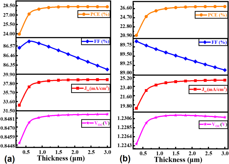
Figure 2 shows the influence of thickness variation on the solar cell performance parameters in the range of 0.3–3.0 μm at constant values of the rest all other parameters as declared in Tables 1 and 2 at 300 K. The cell's PCE increased from 23.9 to 28.5% and 20.9 to 26.6 with the increase of Sb2Se3 and Sb2S3 absorber thickness from 0.3‒ 3.0 μm, respectively. The Jsc increased linearly first in both devices corresponding to the absorber layer thickness of ≤0.75 μm and then it reached a saturated value of 38 and 24 mA/cm2, in contrast, the FF tends to decrease almost linearly for Sb2Se3 and Sb2S3 absorber, respectively. This increment of Jsc is owing to the marked improvement of photon absorption at thicker Sb2Se3 or Sb2S3 absorber layer. This is reasonable because a thicker absorber has a greater number of photons to produce higher electron-hole pairs (EHPs) [69,80].
Figure 2.
Effect of absorber layer thickness (a) Sb2Se3 and (b) Sb2S3 on the PV parameters.
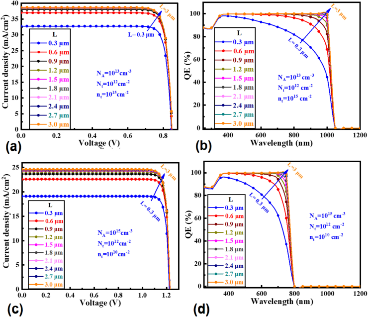
In Figure 3, the quantum efficiency (QE) response of the corresponding solar cells at different absorber thicknesses also reveals similar consequences as observed in Jsc. Further, an increase of cell resistance, as well as diffusion length at thicker absorber layer, causes the decrease of FF [69,81]. In addition, a negligible change in Voc from 0.845‒ 0.848 V and 1.22–1.23 V for Sb2Se3 and Sb2S3 absorbers are observed, respectively. Thus, the highest PCE of 28.5 and 26.6% were observed at a Sb2Se3 and Sb2S3 absorber thickness of 1.2 μm at adjusted photovoltaic parameters values, which is chosen for further investigation.
Figure 3.
Impact of the absorber layer thickness of (a, b) Sb2Se3, and (c, d) Sb2S3 solar cells on the JV and QE, respectively.
3.1.2. Doping concentration effect
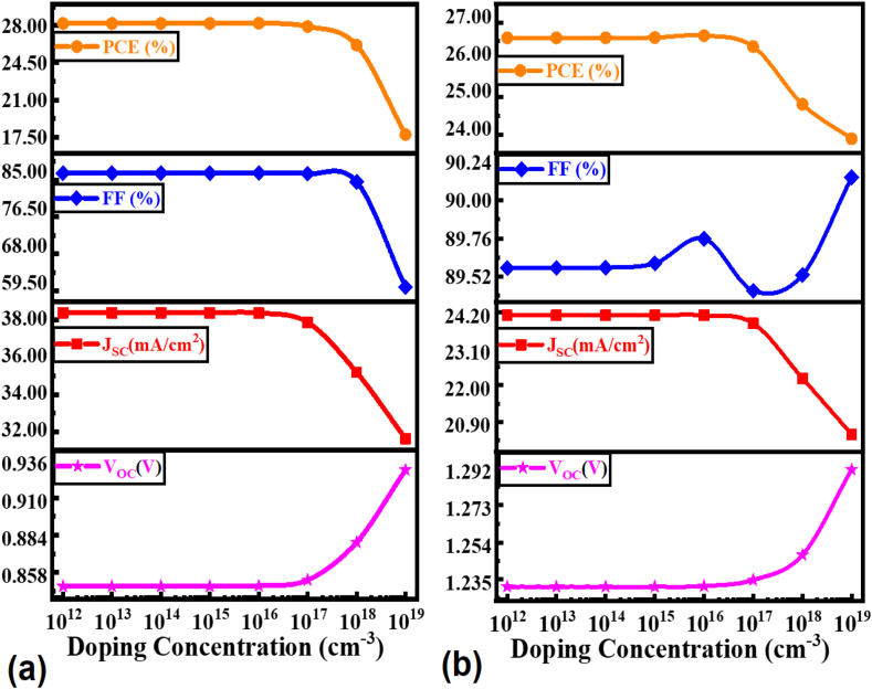
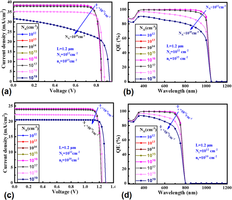
Figure 4 illustrates the impact of doping concentration NA of Sb2Se3 and Sb2S3 absorber layer varied in the range of 1012–1019 cm−3 at 300 K on the solar cell parameters at a constant value of the rest others parameters as summarized in Tables 1 and 2. The change of each output parameter was affected negligibly by varied NA to a value of 1017 cm−3. The Jsc dropped significantly from ∼39.0 to 31.0 mA/cm2 and ∼25.0 to 20.0 mA/cm2 and FF reduced from 85.0 to 59.0% and 85.0 to 59.0%, in contrast, Voc increased from 840 to 930 mV and 1230–1295 mV for Sb2Se3 and Sb2S3 absorber respectively. The decrease of photocurrent at higher acceptor concentration owing to the domination of recombination of photogenerated hole pairs at higher carrier density. The increase of Voc originated from the improved build-in-potential by further lowering fermi-level at higher acceptor concentration and thereby larger band offset compare with lower doping level at the absorber/buffer interface. Therefore, a sharp decrease in JSC and therefore the PCE is observed. By adjusting the PV parameters value, the optimum NA was found at 1013 and 1015 cm−3 for Sb2Se3 and Sb2S3 absorbers, respectively. Thus, the PCE of 28.20 and 26.6%, VOC of 840 and 1230 mV, JSC of 38.40 and 24.11 mA/cm2, FF of 86.55 and 89.6% at an optimum NA value for Sb2Se3 and Sb2S3 absorbers, respectively.
Figure 4.
Effect of the doping concentration of (a) Sb2Se3, and (b) Sb2S3 absorber layer on the solar cell performance parameters.
Figure 5 shows the impact of the doping concentration of Sb2Se3 and Sb2S3 absorber layers on the JV and QE spectra of the corresponding solar cells, respectively. The response of QE reduces markedly in the case of both absorber configurations when the hole doping level exceeds 1017 cm−3 which further reveals the recombination of the photogenerated carrier as expected from an increase in the recombination of free carrier charges within the bulk. The lower energy (longer wavelength) photons are absorbed noticeably in the absorber layer. Consequently, a dramatic impact of the doping concentration on the collected conversion efficiency was observed [82].
Figure 5.
Impact of the absorber layer doping concentration of (a, b) Sb2Se3, and (c, d) Sb2S3 solar cells on the JV and QE, respectively.
3.1.3. Effect of the carrier concentration of the absorber layer on the G-R profile
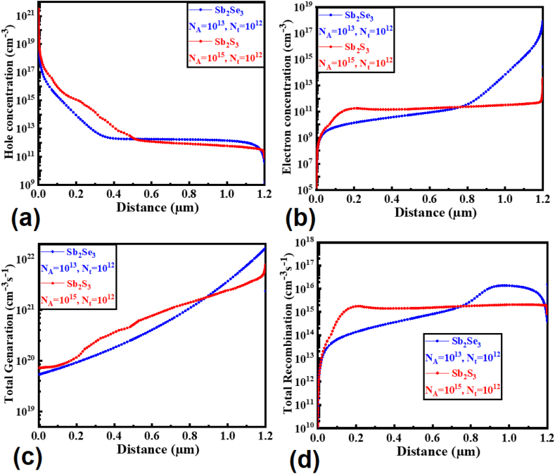
Figure 6 demonstrates the influence of carrier (electron and hole) concentration and total generation-recombination (G-R) profiles as a function of Sb2Se3 and Sb2S3 absorber layer thickness. The effective density of states (DOS) in the valence bands, the hole concentration of Sb2S3 is slightly larger than that of Sb2Se3 owing to the difference in acceptor concentration in the absorbers, and. In contrast, the electron concentration of the Sb2S3 absorber is lower than that of the Sb2Se3 absorber. The carrier generation and recombination profiles obtained by a systematic study revealed the potentiality of each Sb-chalcogenides-based absorber of Sb2S3 and Sb2Se3 compare with reported inorganic, organic, and compound semiconductor materials used as an absorber at a specified and adjusted carrier concentration and defect density [[83], [84], [85], [86], [87]]. Thus, Sb-chalcogenides-based Sb2S3 and Sb2Se3 appear of much more promising and efficient absorber materials, which can be used for the fabrication of high-performance thin film solar cells with lower e-h recombination, in contrast, higher carrier generation.
Figure 6.
Influence of (a) hole and (b) electron carrier concentration, and total (c) generation and (d) recombination concerning the absorber layer thicknesses.
3.2. Impact of WS2 ETL layer on the photovoltaic performance
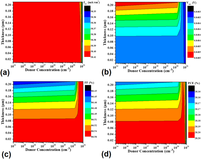
Figure 7 shows the effect of thickness and doping concentration of WS2 ETL on the performance of Sb2Se3-based solar cell devices in the range of 0.01–0.21 μm and 1014–1021 cm−3 respectively, keeping unchanged all other associated parameters as summarized in Tables 1 and 2. The VOC increases from 0.8483 to 0.9293 V, while the JSC decreases from 38.40 to 31.63 mA/cm2 with an increase of donor concentration from 1012 to 1019 cm−3. The increment of VOC originated from the improved electric field with higher resultant Vbi developed at higher donor concentration in WS2 ETL. On the other hand, the availability of a higher density of carriers causes a larger recombination rate of photogenerated carriers, consequently reducing JSC [88,89]. In addition, an insignificant impact of donor concentration on FF was observed. However, fewer photons may reach the absorber layer when the ETL thickness increases, resulting in a reduction in EHP generation due to parasitic absorption by the ETL itself. Consequently, the JSC and the PCE of both the solar cells tend to decrease [36,69,81]. Thus, the highest PCE of ∼29.0% was observed at WS2 ETL thickness of ∼0.03 μm and carrier concentration of ≤ 1017 cm−3.
Figure 7.
Impact of thickness and doping concentration of WS2 ETL on the photovoltaic performance (a) Jsc, (b) Voc, (c) FF, and (d) PCE of Sb2Se3-based solar cell.
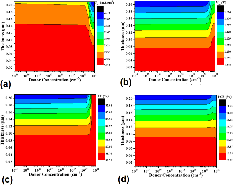
Figure 8 demonstrates the impact of thickness and doping concentration of WS2 ETL on the performance of Sb2S3-based solar cells in the range of 0.01–0.21 μm and 1014–1021 cm−3 respectively, at a constant of all other parameters as summarized in Tables 1 and 2. The VOC increases from 1.21 to 1.23 V, in contrast, the JSC decreases from 24.11 to 20.52 mA/cm2 with the increase of donor concentration from 1012 to 1019 cm−3. The increment of VOC originated by the improved electric field with enhanced resultant Vbi developed at higher donor concentration in WS2 ETL as observed in the case of Sb2S3-based cells. On the other hand, higher carrier density causes increased recombination of photogenerated carriers, consequently, reduced JSC observed. The photons of longer wavelengths are deeply absorbed in the absorber layer at higher doping concentration owing to a smaller mean free path at a higher carrier density state.
Figure 8.
Impact of thickness and doping concentration of WS2 ETL on the photovoltaic performance (a) Jsc, (b) Voc, (c) FF, and (d) PCE of Sb2S3-based solar cell.
Thus, the optimum thickness of WS2 ETL was found of 0.03 μm with a donor concentration of 1017 and 1018 cm−3 for both Sb2Se3 and Sb2S3 absorber-based heterostructures, respectively, considering the tradeoff condition among solar cell parameters.
3.3. Influence of the bulk and interface defect density on the PV performance
Defects are mainly originated from dislocations and grain boundaries (GBs) in the synthesized layers. The defect density reduces the carrier lifetime and mobility markedly, which in turn acts as a carrier trapping center or carrier recombination [90]. Thus, cell performance is significantly affected. A detailed study on the impact of bulk and interface defect density has been performed in this section.
3.3.1. Effect of the absorber's bulk defect density
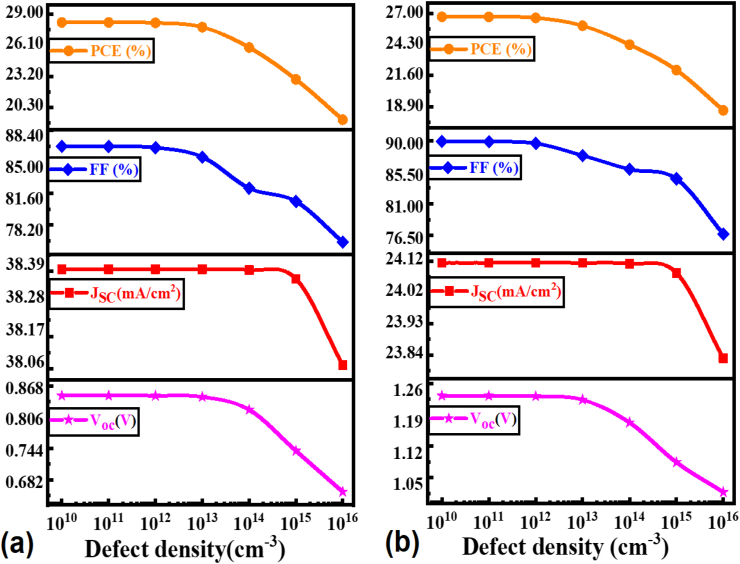
The influence of the bulk defect density of the Sb2Se3 and Sb2S3 absorber layers on the PV parameters was explored in this section, and the findings are presented in Figure 9.
Figure 9.
Impact of the bulk defect density of (a) Sb2Se3, and (b) Sb2S3 absorber layer on the photovoltaic performance.
The carrier recombination rate in the p-type materials can be defined by Eq. (6) [90],
| (6) |
where K3, K2, and K1 are the 1st, 2nd, and 3rd order decay constant. Herein, ki (i = 1,2,3) refers to an interaction between i carriers (electrons/holes/excitons, depending on the species corresponding to the feature). The k3 represents Auger recombination whereby a third carrier absorbs the energy released from a recombination event and so on, k2 represents bimolecular recombination with exciton-exciton annihilation, k1 corresponds either recombination of excitons or recombination between a free carrier and a trapped (localized) carrier [91]. The maximum power loss in the solar cell is due to the non-radiative SRH recombination process [90,92,93] and the defects in the absorber layer mostly cause the SRH recombination, which is generally defined by Eq. (7),
| (7) |
where τ, Et, k, and T represent the charge carrier lifetime, defect energy level within the bandgap, Boltzmann constant, and solar cell operating temperature, respectively. However, carrier lifetime (τ) has been calculated using the following Eq. (8) [76],
| (8) |
where σ, Nt, and Vth represent the capture cross-section area of the charge carrier, defect concentration, and charge carrier thermal velocity, respectively.
In Figure 9, the PCE is almost unchanged with a defect density of 1013 cm−3 and 1012 cm−3 for the Sb2Se3 and Sb2S3-based devices. The FF, VOC, and JSC decreased noticeably, and consequently, the PCE decreased from 28 to 18% and from 27 to 19% in Sb2Se3 and Sb2S3-based solar cells corresponding to defect density of 1010–1016 cm−3. Higher SRH-recombination rate is dominant at a defect density of ≥ 1013 cm−3 which deteriorates the cell performance markedly [67]. Thus, a defect density level of < 1013 cm−3 is required to achieve the highest cell performance.
3.3.2. Effect of the WS2 ETL's bulk defect density
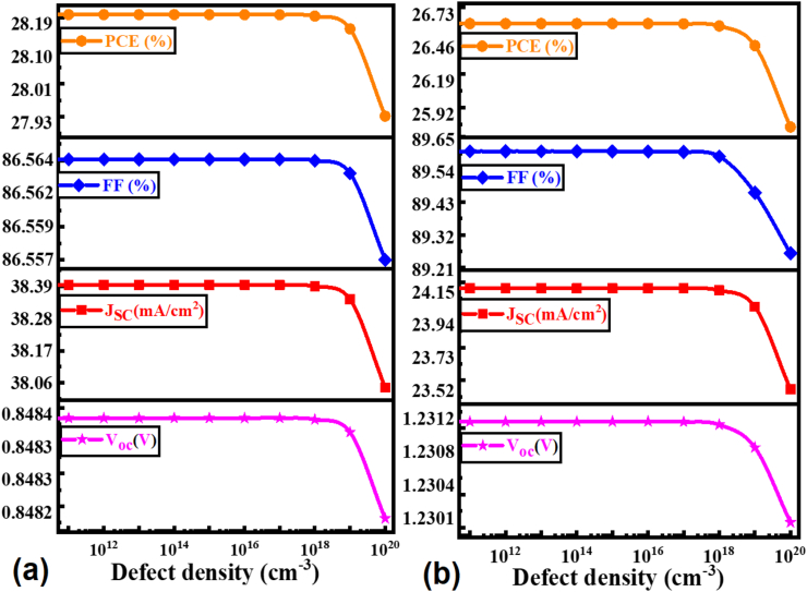
Figure 10 shows the impacts of ETL's bulk defect density on the solar cell's parameters in the range of 1010‒ 1020 cm−3, while all other parameters remained unchanged as summarized in Tables 1 and 2. It's worth noting that the PV performance metrics of both solar cells degrade noticeably with increased ETL defects. Even though the values of the designed two solar cells' cell parameters are different in magnitude, the trend of lowering the cell performance is very similar to an increase in defects level. Although the PCE retains constant at the highest value up to 1018 cm−3, it decreases linearly from ∼28 to ∼18% and from ∼27.0 to ∼19% when the defect increases from 1018 to 1020 cm−3. Thus, the defect density is required to be 1018 cm−3 for achieving the highest cell performance.
Figure 10.
Impact of the WS2 ETL bulk defect density on the photovoltaic performance of (a) Sb2Se3, and (b) Sb2S3 solar cells.
3.3.3. Effect of the ETL/absorber interface defect density
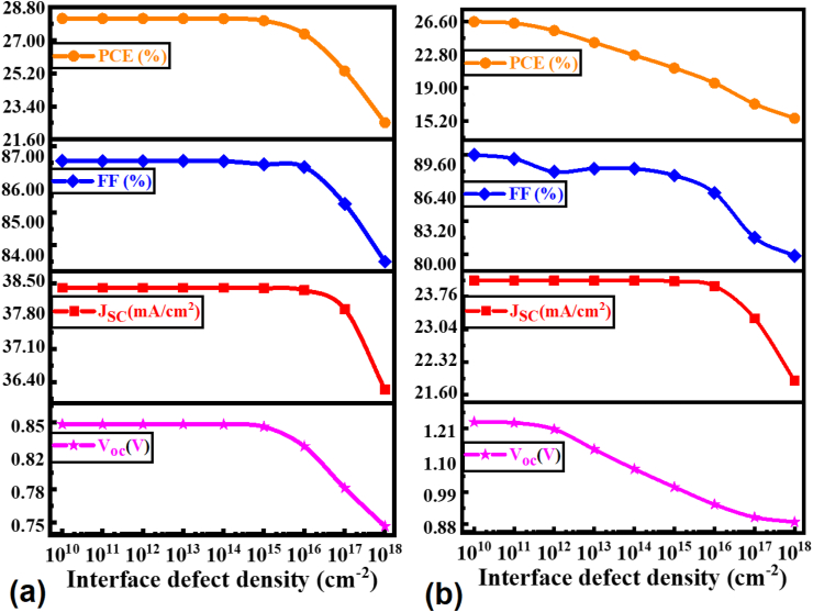
Figure 11 demonstrate the influence of the interface defect density of the ETL/absorber interface on device performance at the defect density of 1010–1018 cm−2 at a WT of 300 K, at an unchanged other parameters value as described in Tables 1 and 2.
Figure 11.
Influence of the ETL/absorber interface defect density on the device performance of (a) Sb2Se3, and (b) Sb2S3 solar cells.
The impact of defect density on cell performance is almost negligible until the interface defect density reaches 1015 cm−2 for the WS2/Sb2Se3 interface and 1011 cm−3 for the WS2/Sb2S3 interface. As perceived from Figure 11, the interface of the Sb2S3 solar cell has a more critical impact on the PV characteristics than the Sb2Se3 solar cell beyond these marginal values in both devices. All of the metrics drop dramatically as their charge carriers recombine notably with the opposing charge carriers before reaching the junction and at a lower rate of creating EHPs [6,81].
In addition, the effect of temperature variation of Sb2Se3 and Sb2S3 based heterojunction solar cell is shown in Figure S1. It has been revealed that at high temperatures, the efficiency of Sb2Se3 and Sb2S3 based heterojunction solar cell reduces, which is consistent with the reported works as well [94].
3.4. The J-V and QE spectra of the optimized solar cells
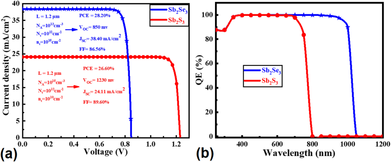
The current density-voltage (J- V) curve and the corresponding QE spectrum as a function of the light wavelength of the optimized HJSCs are shown in Figure 12. In Figure 12(a), the simulation results of voltage (VOC), current (JSC), fill factor (FF) and efficiency (ɳ) of the optimized Sb2Se3 (Sb2S3) proposed solar cells is 850 mV (1230 mV), 38.40 mA/cm2 (26.60 mA/cm2), 86.56% (89.60%) and 28.20% (24.11%), respectively. Figure 12(b) reveals that the QE of the Sb2Se3 (Sb2S3) structure falls to almost 0% at the wavelength of 800 nm (1050 nm), while it is over 97% at a lower value of these wavelength values for Sb2Se3 and Sb2S3 HJSCs. The degree of current improvement depends on the band gap of the absorber material, reversely, the value of Voc enhanced due to the generation of high built-in potential at the absorber interface, therefore, having an almost ideal band gap for absorbing visible spectra significantly, Sb2Se3 and Sb2S3 appeal great attention for the fabrication of high-efficiency HJSCs [59,65,67].
Figure 12.
The (a) J-V characteristics, and (b) QE spectra of the proposed Sb2Se3 and Sb2S3 heterojunction solar cells.
Table 3 compares PV performance to previously report experimental and simulation studies. The simulation may be easily verified because the results are consistent with prior studies and are within the SQ limit for single-junction solar cells. Both solar cells proposed here, however, outperform the devices proposed previously [24,61,[64], [65], [66], [67]].
Table 3.
Optimized PV parameters of the proposed HJSCs with comparison to similar HJSCs in the literature. [Theo. = Theoretical SQ limit, Exp. = Experimental, Sim. = Simulation].
| Absorber material | Types | Junction Formed | JSC (mA/cm2) | VOC (mV) | FF (%) | PCE (%) | Ref. |
|---|---|---|---|---|---|---|---|
| Sb2Se3 | Theo. | Homo | 39.99 | 935 | 87.70 | 32.74 | [95] |
| Exp. | Hetero | 30.80 | 423 | 58.10 | 7.50 | [96] | |
| Exp. | Hetero | 32.58 | 400 | 70.30 | 9.20 | [97] | |
| Exp. | Hetero | 30.86 | 488 | 67.19 | 10.12 | [98] | |
| Sim. | Hetero | 38.15 | 410 | 74.08 | 11.52 | [65] | |
| Sim. | Hetero | 38.40 | 850 | 86.56 | 28.20 | ∗ | |
| Sb2S3 | Theo. | Homo | 25.47 | 1309 | 90.50 | 30.14 | [95] |
| Exp. | Hetero | 14.73 | 645 | 65.69 | 6.27 | [61] | |
| Exp. | Hetero | 15.29 | 748 | 57.07 | 6.53 | [64] | |
| Sim. | Hetero | 23.73 | 970 | 72.32 | 16.65 | [24] | |
| Sim. | Hetero | 24.00 | 1230 | 89.60 | 26.60 | ∗ |
This work.
4. Conclusions
The sb-chalcogenides of Sb2Se3 and Sb2S3-based high-efficiency HJSCs with WS2 ETL were investigated numerically using SCAPS-1D solar cell simulator. While comprehensive optimization research was carried out, their photovoltaic performance was compared to that found in the literature. The highest PCE of 28.20% with VOC of 850 mV, JSC of 38.40 mA/cm2, and FF of 86.56% was obtained from Sb2Se3 absorber-based heterostructure, while the highest PCE of 26.60% with VOC of 1230 mV, JSC of 26.60 mA/cm2, and FF of 89.60% was obtained from Sb2S3 absorber based heterostructure together with WS2 ETL layer. Simulation results indicate that WS2 could be a competitive ETL for fabricating low-toxicity, cost-effective, and highly efficient Sb2Se3 and Sb2S3-based HJSCs for harnessing solar energy. Furthermore, these devices' higher performance compared with previous reports reveals the high potentiality of Sb-chalcogenide as an absorber material that could be efficient one to realize both high-efficiency high-current (HEHC) and high-efficiency high-voltage (HEHV) solar panels.
Declarations
Author contribution statement
Md. Ferdous Rahman: Conceived and designed the experiments; Performed the experiments; contributed reagents, materials, analysis tools or data; analyzed and interpreted the data; wrote the paper.
Md. Mahabub Alam Moon, Md. Hasan Ali, Md. Dulal Haque, Abdul Kuddus, Jaker Hossain and Abu Bakar Md. Ismail: analyzed and interpreted the data; wrote the paper.
M. Khalid Hossain: Conceived and designed the experiments; analyzed and interpreted the data; wrote the paper.
Funding statement
Prof. Dr. Md. Ferdous Rahman was partially supported by an innovation fund from the ICT Division, Govt. of Bangladesh [Grant No. 22IF15426 (2021–2022)].
Data availability statement
Data will be made available on request.
Declaration of interest's statement
The authors declare no conflict of interest.
Additional information
No additional information is available for this paper.
Acknowledgments
The authors are thankful to Marc Burgleman and his colleagues at the University of Electronics and Information Systems (ELIS), Department of Electronics and Information Systems, Belgium, for supplying the SCAPS software package, version 3.3.07.
Contributor Information
Md. Ferdous Rahman, Email: ferdous@brur.ac.bd.
Md. Mahabub Alam Moon, Email: mmamoon9357@gmail.com.
M. Khalid Hossain, Email: khalid.baec@gmail.com, khalid@kyudai.jp.
Appendix A. Supplementary data
The following is the supplementary data related to this article:
References
- 1.Wang X., Tang R., Wu C., Zhu C., Chen T. Development of antimony sulfide–selenide Sb2(S, Se)3-based solar cells. J. Energy Chem. 2018;27:713–721. [Google Scholar]
- 2.Hossain M.K., Raihan G.A., Akbar M.A., Kabir Rubel M.H., Ahmed M.H., Khan M.I., Hossain S., Sen S.K., Jalal M.I.E., El-Denglawey A. Current applications and future potential of rare earth oxides in sustainable nuclear, radiation, and energy devices: a review. ACS Appl. Electron. Mater. 2022;4:3327–3353. [Google Scholar]
- 3.Green M.A. How did solar cells get so cheap? Joule. 2019;3:631–633. [Google Scholar]
- 4.Hossain M.K., Pervez M.F., Tayyaba S., Uddin M.J., Mortuza A.A., Mia M.N.H., Manir M.S., Karim M.R., Khan M.A. Efficiency enhancement of natural dye sensitized solar cell by optimizing electrode fabrication parameters. Mater. Sci. 2017;35:816–823. [Google Scholar]
- 5.Hossain M.K., Pervez M.F., Mia M.N.H., Mortuza A.A., Rahaman M.S., Karim M.R., Islam J.M.M., Ahmed F., Khan M.A. Effect of dye extracting solvents and sensitization time on photovoltaic performance of natural dye sensitized solar cells. Results Phys. 2017;7:1516–1523. [Google Scholar]
- 6.Biplab S.R.I., Ali M.H., Moon M.M.A., Pervez M.F., Rahman M.F., Hossain J. Performance enhancement of CIGS-based solar cells by incorporating an ultrathin BaSi2 BSF layer. J. Comput. Electron. 2020;19:342–352. [Google Scholar]
- 7.Hossain M.K., Mortuza A.A., Sen S.K., Basher M.K., Ashraf M.W., Tayyaba S., Mia M.N.H., Uddin M.J. A comparative study on the influence of pure anatase and Degussa-P25 TiO2 nanomaterials on the structural and optical properties of dye sensitized solar cell (DSSC) photoanode. Optik. 2018;171:507–516. [Google Scholar]
- 8.Hossain M.K., Pervez M.F., Uddin M.J., Tayyaba S., Mia M.N.H., Bashar M.S., Jewel M.K.H., Haque M.A.S., Hakim M.A., Khan M.A. Influence of natural dye adsorption on the structural, morphological and optical properties of TiO2 based photoanode of dye-sensitized solar cell. Mater. Sci. 2017;36:93–101. [Google Scholar]
- 9.Sen S., Ganguly S., Das A., Sen J., Dey S. Renewable energy scenario in India: opportunities and challenges. J. Afr. Earth Sci. 2016;122:25–31. [Google Scholar]
- 10.Qarony W., Hossain M.I., Hossain M.K., Uddin M.J., Haque A., Saad A.R., Tsang Y.H. Efficient amorphous silicon solar cells: characterization, optimization, and optical loss analysis. Results Phys. 2017;7:4287–4293. [Google Scholar]
- 11.Hossain M.I., Qarony W., Hossain M.K., Debnath M.K., Uddin M.J., Tsang Y.H. Effect of back reflectors on photon absorption in thin-film amorphous silicon solar cells. Appl. Nanosci. 2017;7:489–497. [Google Scholar]
- 12.Basher M.K., Mishan R., Biswas S., Hossain M.K., Akand M.A.R., Matin M.A. Study and analysis the Cu nanoparticle assisted texturization forming low reflective silicon surface for solar cell application. AIP Adv. 2019;9 [Google Scholar]
- 13.Basher M.K., Hossain M.K., Uddin M.J., Akand M.A.R., Shorowordi K.M. Effect of pyramidal texturization on the optical surface reflectance of monocrystalline photovoltaic silicon wafers. Optik. 2018;172:801–811. [Google Scholar]
- 14.Biswas S., Basher M.K., Hossain M.K., Akand M.A.R., Rahman M.T., Ahmed M.R., Matin M.A., Huque S. Study and analysis of the morphological, elemental and electrical properties of phosphorus doped monocrystalline silicon solar cell. Mater. Res. Express. 2019;6 [Google Scholar]
- 15.Basher M.K., Uddin M.J., Hossain M.K., Akand M.A.R., Biswas S., Mia M.N.H., Shorowordi K.M. Effect of doping profile on sheet resistance and contact resistance of monocrystalline silicon solar cells. Mater. Res. Express. 2019;6 [Google Scholar]
- 16.Hossain M.K.K., Pervez M.F.F., Mia M.N.H.N.H., Tayyaba S., Uddin M.J.J., Ahamed R., Khan R.A.A., Hoq M., Khan M.A.A., Ahmed F. Annealing temperature effect on structural, morphological and optical parameters of mesoporous TiO2 film photoanode for dye-sensitized solar cell application. Mater. Sci. 2017;35:868–877. [Google Scholar]
- 17.Hossain M.K., Rahman M.T., Basher M.K., Manir M.S., Bashar M.S. Influence of thickness variation of gamma-irradiated DSSC photoanodic TiO2 film on structural, morphological and optical properties. Optik. 2019;178:449–460. [Google Scholar]
- 18.Hossain M.K., Rahman M.T., Basher M.K., Afzal M.J., Bashar M.S. Impact of ionizing radiation doses on nanocrystalline TiO2 layer in DSSC’s photoanode film. Results Phys. 2018;11:1172–1181. [Google Scholar]
- 19.Ganose A.M., Savory C.N., Scanlon D.O. Beyond methylammonium lead iodide: prospects for the emergent field of ns 2 containing solar absorbers. Chem. Commun. 2017;53:20–44. doi: 10.1039/c6cc06475b. [DOI] [PubMed] [Google Scholar]
- 20.Tyagi V.V., Rahim N.A.A., Rahim N.A., Selvaraj J.A./L. Progress in solar PV technology: research and achievement. Renew. Sustain. Energy Rev. 2013;20:443–461. [Google Scholar]
- 21.Hosenuzzaman M., Rahim N.A., Selvaraj J., Hasanuzzaman M., Malek A.B.M.A., Nahar A. Global prospects, progress, policies, and environmental impact of solar photovoltaic power generation. Renew. Sustain. Energy Rev. 2015;41:284–297. [Google Scholar]
- 22.Bencherif H., Meddour F., Elshorbagy M.H., Khalid Hossain M., Cuadrado A., Abdi M.A., Bendib T., Kouda S., Alda J. Performance enhancement of (FAPbI3)1-x(MAPbBr3)x perovskite solar cell with an optimized design. Micro and Nanostructures. 2022;171 [Google Scholar]
- 23.Alharbi F.H., Kais S. Theoretical limits of photovoltaics efficiency and possible improvements by intuitive approaches learned from photosynthesis and quantum coherence. Renew. Sustain. Energy Rev. 2015;43:1073–1089. [Google Scholar]
- 24.Green M.A., Hishikawa Y., Dunlop E.D., Levi D.H., Hohl-Ebinger J., Ho-Baillie A.W.Y. Solar cell efficiency tables (version 51) Prog. Photovoltaics Res. Appl. 2018;26:3–12. [Google Scholar]
- 25.Jackson P., Wuerz R., Hariskos D., Lotter E., Witte W., Powalla M. Effects of heavy alkali elements in Cu(In,Ga)Se2 solar cells with efficiencies up to 22.6. Phys. Status Solidi Rapid Res. Lett. 2016;10:583–586. [Google Scholar]
- 26.Zakutayev A. Brief review of emerging photovoltaic absorbers. Curr. Opin. Green Sustain. Chem. 2017;4:8–15. [Google Scholar]
- 27.Rahman M.F., Habib M.J.A., Ali M.H., Rubel M.H.K., Islam M.R., Ismail A.B.M., Hossain M.K. Design and numerical investigation of cadmium telluride (CdTe) and iron silicide (FeSi2) based double absorber solar cells to enhance power conversion efficiency. AIP Adv. 2022;12 [Google Scholar]
- 28.Chantana J., Uegaki H., Minemoto T. Influence of Na in Cu2SnS3 film on its physical properties and photovoltaic performances. Thin Solid Films. 2017;636:431–437. [Google Scholar]
- 29.Jin X., Zhang L., Jiang G., Liu W., Zhu C. High open-circuit voltage of ternary Cu2GeS3 thin film solar cells from combustion synthesized Cu-Ge alloy. Sol. Energy Mater. Sol. Cells. 2017;160:319–327. [Google Scholar]
- 30.Umehara M., Takeda Y., Motohiro T., Sakai T., Awano H., Maekawa R. Cu2Sn1-xGexS3 (x=0.17) thin-film solar cells with high conversion efficiency of 6.0. APEX. 2013;6 [Google Scholar]
- 31.Xue D.-J., Liu S.-C., Dai C.-M., Chen S., He C., Zhao L., Hu J.-S., Wan L.-J. GeSe thin-film solar cells fabricated by self-regulated rapid thermal sublimation. J. Am. Chem. Soc. 2017;139:958–965. doi: 10.1021/jacs.6b11705. [DOI] [PubMed] [Google Scholar]
- 32.Septina W., Ikeda S., Iga Y., Harada T., Matsumura M. Thin film solar cell based on CuSbS2 absorber fabricated from an electrochemically deposited metal stack. Thin Solid Films. 2014;550:700–704. [Google Scholar]
- 33.Xue D.-J., Yang B., Yuan Z.-K., Wang G., Liu X., Zhou Y., Hu L., Pan D., Chen S., Tang J. CuSbSe2 as a potential photovoltaic absorber material: studies from theory to experiment. Adv. Energy Mater. 2015;5 [Google Scholar]
- 34.Hartnauer S., Körbel S., Marques M.A.L., Botti S., Pistor P., Scheer R. Research update: stable single-phase Zn-rich Cu2ZnSnSe4 through in doping. Apl. Mater. 2016;4 [Google Scholar]
- 35.Luo L., Luan W., Yuan B., Zhang C., Jin L. High efficient and stable solid solar cell: based on FeS2 nanocrystals and P3HT: PCBM. Energy Proc. 2015;75:2181–2186. [Google Scholar]
- 36.Moon M.M.A., Ali M.H., Rahman M.F., Hossain J., Ismail A.B.M. Design and simulation of FeSi2-based novel heterojunction solar cells for harnessing visible and near-infrared light. Phys. Status Solidi. 2020;217 [Google Scholar]
- 37.Razykov T.M., Boltaev G.S., Bosio A., Ergashev B., Kouchkarov K.M., Mamarasulov N.K., Mavlonov A.A., Romeo A., Romeo N., Tursunkulov O.M., Yuldoshov R. Characterisation of SnSe thin films fabricated by chemical molecular beam deposition for use in thin film solar cells. Sol. Energy. 2018;159:834–840. [Google Scholar]
- 38.Tang R., Zheng Z.-H., Su Z.-H., Li X.-J., Wei Y.-D., Zhang X.-H., Fu Y.-Q., Luo J.-T., Fan P., Liang G.-X. Highly efficient and stable planar heterojunction solar cell based on sputtered and post-selenized Sb2Se3 thin film. Nano Energy. 2019;64 [Google Scholar]
- 39.Tang R., Wang X., Jiang C., Li S., Jiang G., Yang S., Zhu C., Chen T. Vacuum assisted solution processing for highly efficient Sb2S3 solar cells. J. Mater. Chem. A. 2018;6:16322–16327. [Google Scholar]
- 40.Lu S., Zhao Y., Chen C., Zhou Y., Li D., Li K., Chen W., Wen X., Wang C., Kondrotas R., Lowe N., Tang J. Sb2Se3 thin-film photovoltaics using aqueous solution sprayed SnO2 as the buffer layer. Adv. Electron. Mater. 2018;4 [Google Scholar]
- 41.Chen S., Liu T., Zheng Z., Ishaq M., Liang G., Fan P., Chen T., Tang J. Recent progress and perspectives on Sb2Se3-based photocathodes for solar hydrogen production via photoelectrochemical water splitting. J. Energy Chem. 2022;67:508–523. [Google Scholar]
- 42.Liang G.-X., Luo Y.-D., Chen S., Tang R., Zheng Z.-H., Li X.-J., Liu X.-S., Liu Y.-K., Li Y.-F., Chen X.-Y., Su Z.-H., Zhang X.-H., Ma H.-L., Fan P. Sputtered and selenized Sb2Se3 thin-film solar cells with open-circuit voltage exceeding 500 mV. Nano Energy. 2020;73 [Google Scholar]
- 43.Luo Y.-D., Tang R., Chen S., Hu J.-G., Liu Y.-K., Li Y.-F., Liu X.-S., Zheng Z.-H., Su Z.-H., Ma X.-F., Fan P., Zhang X.-H., Ma H.-L., Chen Z.-G., Liang G.-X. An effective combination reaction involved with sputtered and selenized Sb precursors for efficient Sb2Se3 thin film solar cells. Chem. Eng. J. 2020;393 [Google Scholar]
- 44.Chen S., Liu T., Chen M., Ishaq M., Tang R., Zheng Z., Su Z., Li X., Qiao X., Fan P., Liang G. Crystal growth promotion and interface optimization enable highly efficient Sb2Se3 photocathodes for solar hydrogen evolution. Nano Energy. 2022;99 [Google Scholar]
- 45.Chen C., Li W., Zhou Y., Chen C., Luo M., Liu X., Zeng K., Yang B., Zhang C., Han J., Tang J. Optical properties of amorphous and polycrystalline Sb2Se3 thin films prepared by thermal evaporation. Appl. Phys. Lett. 2015;107 [Google Scholar]
- 46.Costa M.B., de Souza Lucas F.W., Mascaro L.H. Thermal treatment effects on electrodeposited Sb 2 Se 3 photovoltaic thin films. Chemelectrochem. 2017;4:2507–2514. [Google Scholar]
- 47.Lai Y., Chen Z., Han C., Jiang L., Liu F., Li J., Liu Y. Preparation and characterization of Sb2Se3 thin films by electrodeposition and annealing treatment. Appl. Surf. Sci. 2012;261:510–514. [Google Scholar]
- 48.Zhou Y., Leng M., Xia Z., Zhong J., Song H., Liu X., Yang B., Zhang J., Chen J., Zhou K., Han J., Cheng Y., Tang J. Solution-processed antimony selenide heterojunction solar cells. Adv. Energy Mater. 2014;4 [Google Scholar]
- 49.Madelung O. Springer Berlin Heidelberg; Berlin, Heidelberg: 2004. Semiconductors: Data Handbook. [Google Scholar]
- 50.Liang G.-X., Zheng Z.-H., Fan P., Luo J.-T., Hu J.-G., Zhang X.-H., Ma H.-L., Fan B., Luo Z.-K., Zhang D.-P. Thermally induced structural evolution and performance of Sb2Se3 films and nanorods prepared by an easy sputtering method. Sol. Energy Mater. Sol. Cells. 2018;174:263–270. [Google Scholar]
- 51.Li K., Kondrotas R., Chen C., Lu S., Wen X., Li D., Luo J., Zhao Y., Tang J. Improved efficiency by insertion of Zn1−xMgxO through sol-gel method in ZnO/Sb2Se3 solar cell. Sol. Energy. 2018;167:10–17. [Google Scholar]
- 52.Chen C., Zhao Y., Lu S., Li K., Li Y., Yang B., Chen W., Wang L., Li D., Deng H., Yi F., Tang J. Accelerated optimization of TiO2/Sb2Se3 thin film solar cells by high-throughput combinatorial approach. Adv. Energy Mater. 2017;7 [Google Scholar]
- 53.Messina S., Nair M.T.S., Nair P.K. Antimony selenide absorber thin films in all-chemically deposited solar cells. J. Electrochem. Soc. 2009;156:H327. [Google Scholar]
- 54.Itzhaik Y., Niitsoo O., Page M., Hodes G. Sb2S3-Sensitized nanoporous TiO2 solar cells. J. Phys. Chem. C. 2009;113:4254–4256. [Google Scholar]
- 55.Li Z., Liang X., Li G., Liu H., Zhang H., Guo J., Chen J., Shen K., San X., Yu W., Schropp R.E.I., Mai Y. 9.2%-efficient core-shell structured antimony selenide nanorod array solar cells. Nat. Commun. 2019;10:125. doi: 10.1038/s41467-018-07903-6. [DOI] [PMC free article] [PubMed] [Google Scholar]
- 56.Ning H., Guo H., Zhang J., Wang X., Jia X., Qiu J., Yuan N., Ding J. Enhancing the efficiency of Sb2S3 solar cells using dual-functional potassium doping. Sol. Energy Mater. Sol. Cells. 2021;221 [Google Scholar]
- 57.Lin J., Mahmood A., Chen G., Ahmad N., Chen M., Fan P., Chen S., Tang R., Liang G. Crystallographic orientation control and defect passivation for high-efficient antimony selenide thin-film solar cells, Mater. Today Phys. 2022;27 [Google Scholar]
- 58.Tang R., Chen S., Zheng Z., Su Z., Luo J., Fan P., Zhang X., Tang J., Liang G. Heterojunction annealing enabling record open-circuit voltage in antimony triselenide solar cells. Adv. Mater. 2022;34 doi: 10.1002/adma.202109078. [DOI] [PubMed] [Google Scholar]
- 59.Lin L., Jiang L., Qiu Y., Fan B. Analysis of Sb2Se3/CdS based photovoltaic cell: a numerical simulation approach. J. Phys. Chem. Solid. 2018;122:19–24. [Google Scholar]
- 60.Baig F., Khattak Y.H., Beg S., Soucase B.M. Numerical analysis of a novel CNT/Cu2O/Sb2Se3/In2S3/ITO antimony selenide solar cell. Optik. 2019;197 [Google Scholar]
- 61.Gharibshahian I., Orouji A.A., Sharbati S. Alternative buffer layers in Sb2Se3 thin-film solar cells to reduce open-circuit voltage offset. Sol. Energy. 2020;202:294–303. [Google Scholar]
- 62.Xiao Y., Wang H., Kuang H. Numerical simulation and performance optimization of Sb2S3 solar cell with a hole transport layer. Opt. Mater. 2020;108 [Google Scholar]
- 63.Cao Y., Zhu X., Chen H., Zhang X., Zhouc J., Hu Z., Pang J. Towards high efficiency inverted Sb2Se3 thin film solar cells. Sol. Energy Mater. Sol. Cells. 2019;200 [Google Scholar]
- 64.Gharibshahian I., Orouji A.A., Sharbati S. Towards high efficiency Cd-Free Sb2Se3 solar cells by the band alignment optimization. Sol. Energy Mater. Sol. Cells. 2020;212 [Google Scholar]
- 65.Li Z.-Q., Ni M., Feng X.-D. Simulation of the Sb2Se3 solar cell with a hole transport layer. Mater. Res. Express. 2020;7 [Google Scholar]
- 66.Baig F., Khattak Y.H., Shuja A., Riaz K., Soucase B.M. Performance investigation of Sb2Se3 based solar cell by device optimization, band offset engineering and Hole Transport Layer in SCAPS-1D. Curr. Appl. Phys. 2020;20:973–981. [Google Scholar]
- 67.Basak A., Singh U.P. Numerical modelling and analysis of earth abundant Sb2S3 and Sb2Se3 based solar cells using SCAPS-1D. Sol. Energy Mater. Sol. Cells. 2021;230 [Google Scholar]
- 68.Rahman M.F., Hossain J., Kuddus A., Tabassum S., Rubel M.H.K., Rahman M.M., Moriya Y., Shirai H., Ismail A.B.M. A novel CdTe ink-assisted direct synthesis of CdTe thin films for the solution-processed CdTe solar cells. J. Mater. Sci. 2020;55:7715–7730. [Google Scholar]
- 69.Moon M.M.A., Rahman M.F., Kamruzzaman M., Hossain J., Ismail A.B.M. Unveiling the prospect of a novel chemical route for synthesizing solution-processed CdS/CdTe thin-film solar cells. Energy Rep. 2021;7:1742–1756. [Google Scholar]
- 70.Bin Rafiq M.K.S., Amin N., Alharbi H.F., Luqman M., Ayob A., Alharthi Y.S., Alharthi N.H., Bais B., Akhtaruzzaman M. WS2: a new window layer material for solar cell application. Sci. Rep. 2020;10:771. doi: 10.1038/s41598-020-57596-5. [DOI] [PMC free article] [PubMed] [Google Scholar]
- 71.Burgelman M., Nollet P., Degrave S. Modelling polycrystalline semiconductor solar cells. Thin Solid Films. 2000;361–362:527–532. [Google Scholar]
- 72.Decock K., Zabierowski P., Burgelman M. Modeling metastabilities in chalcopyrite-based thin film solar cells. J. Appl. Phys. 2012;111 [Google Scholar]
- 73.Fortunato E., Ginley D., Hosono H., Paine D.C. Transparent conducting oxides for photovoltaics. MRS Bull. 2007;32:242–247. [Google Scholar]
- 74.Gordon R.G. Criteria for choosing transparent conductors. MRS Bull. 2000;25:52–57. [Google Scholar]
- 75.Zhang J., Kondrotas R., Lu S., Wang C., Chen C., Tang J. Alternative back contacts for Sb2Se3 solar cells. Sol. Energy. 2019;182:96–101. [Google Scholar]
- 76.Burgelman M., Decock K., Niemegeers A., Verschraegen J., Degrave S. Univ. Gent.; 2019. SCAPS Manual; pp. 1–111. [Google Scholar]
- 77.Sobayel K., Akhtaruzzaman M., Rahman K.S., Ferdaous M.T., Al-Mutairi Z.A., Alharbi H.F., Alharthi N.H., Karim M.R., Hasmady S., Amin N. A comprehensive defect study of tungsten disulfide (WS2) as electron transport layer in perovskite solar cells by numerical simulation. Results Phys. 2019;12:1097–1103. [Google Scholar]
- 78.Sobayel K., Rahman K.S., Karim M.R., Aijaz M.O., Dar M.A., Shar M.A., Misran H., Amin N. Numerical modeling on prospective buffer layers for tungsten di-sulfide (WS2) solar cells by scaps-1D. Chalcogenide Lett. 2018;15:307–315. [Google Scholar]
- 79.Bencherif H., Hossain M.K. Design and numerical investigation of efficient (FAPbI3)1−x(CsSnI3)x perovskite solar cell with optimized performances. Sol. Energy. 2022;248:137–148. [Google Scholar]
- 80.Hossain M.K., Rubel M.H.K., Toki G.F.I., Alam I., Rahman M.F., Bencherif H. Effect of various electron and hole transport layers on the performance of CsPbI3-based perovskite solar cells: a numerical investigation in DFT, SCAPS-1D, and wxAMPS frameworks. ACS Omega. 2022;7:43210–43230. doi: 10.1021/acsomega.2c05912. [DOI] [PMC free article] [PubMed] [Google Scholar]
- 81.Moon M.M.A., Ali M.H., Rahman M.F., Kuddus A., Hossain J., Ismail A.B.M. Investigation of thin-film p -BaSi2/n-CdS heterostructure towards semiconducting silicide based high efficiency solar cell. Phys. Scripta. 2020;95 [Google Scholar]
- 82.Zyoud S.H., Zyoud A.H., Ahmed N.M., Prasad A.R., Khan S.N., Abdelkader A.F.I., Shahwan M. Numerical modeling of high conversion efficiency FTO/ZnO/CdS/CZTS/MO thin film-based solar cells: using SCAPS-1D software. Crystals. 2021;11:1468. [Google Scholar]
- 83.Cao Y., Liu C., Jiang J., Zhu X., Zhou J., Ni J., Zhang J., Pang J., Rummeli M.H., Zhou W., Liu H., Cuniberti G. Theoretical insight into high-efficiency triple-junction tandem solar cells via the band engineering of antimony chalcogenides. Sol. RRL. 2021;5 [Google Scholar]
- 84.Delahoy A.E., Cheng Z., Chin K.K. Carrier collection in thin-film CdTe solar cells: theory and experiment, 27th. Eur. Photovolt. Sol. Energy Conf. Exhib. 2012:2837–2842. [Google Scholar]
- 85.Benzetta A.E.H., Abderrezek M., Djeghlal M.E. A comparative study on generation and recombination process of kesterite CZTS based thin film solar cells for different designs. Optik. 2020;219 [Google Scholar]
- 86.Atowar Rahman M. Enhancing the photovoltaic performance of Cd-free Cu2ZnSnS4 heterojunction solar cells using SnS HTL and TiO2 ETL. Sol. Energy. 2021;215:64–76. [Google Scholar]
- 87.El Otmani R., El Manouni A., Al Maggoussi A. Numerical simulation of CZTSe based solar cells using different back surface field layers: improvement and comparison. J. Electron. Mater. 2021;50:2021–2033. [Google Scholar]
- 88.Khattak Y.H., Baig F., Ullah S., Marí B., Beg S., Ullah H. Enhancement of the conversion efficiency of thin film kesterite solar cell. J. Renew. Sustain. Energy. 2018;10 [Google Scholar]
- 89.Zahoo R.K., Saleh A.N. Effect of carrier concentration and thickness of absorber layer on performance CBTS solar cell. Turkish J. Comput. Math. Educ. 2021;12:5056–5064. [Google Scholar]
- 90.Ahmmed S., Aktar A., Tabassum S., Rahman M.H., Rahman M.F., Ismail A.B. Md. CuO based solar cell with V2O5 BSF layer: theoretical validation of experimental data. Superlattice. Microst. 2021;151 [Google Scholar]
- 91.Barrette A.G. North Carolina State University; 2018. Ultrafast Optical Studies of Amplified Spontaneous Emission in Hybrid Organic-Inorganic Perovskites.http://www.lib.ncsu.edu/resolver/1840.20/35772 [Google Scholar]
- 92.Ahmmed S., Aktar A., Rahman M.F., Hossain J., Ismail A.B.M. A numerical simulation of high efficiency CdS/CdTe based solar cell using NiO HTL and ZnO TCO. Optik. 2020;223 [Google Scholar]
- 93.Chen J., Park N. Causes and solutions of recombination in perovskite solar cells. Adv. Mater. 2019;31 doi: 10.1002/adma.201803019. [DOI] [PubMed] [Google Scholar]
- 94.Bouich A., Hartiti B., Ullah S., Ullah H., Touhami M.E., Santos D.M.F., Mari B. Experimental, theoretical, and numerical simulation of the performance of CuInxGa(1-x)S2-based solar cells. Optik. 2019;183:137–147. [Google Scholar]
- 95.Rühle S. Tabulated values of the Shockley–Queisser limit for single junction solar cells. Sol. Energy. 2016;130:139–147. [Google Scholar]
- 96.Chang J.A., Rhee J.H., Im S.H., Lee Y.H., Kim H., Il Seok S., Nazeeruddin M.K., Gratzel M. High-performance nanostructured Inorganic−Organic heterojunction solar cells. Nano Lett. 2010;10:2609–2612. doi: 10.1021/nl101322h. [DOI] [PubMed] [Google Scholar]
- 97.Im S.H., Lim C.-S., Chang J.A., Lee Y.H., Maiti N., Kim H.-J., Nazeeruddin M.K., Grätzel M., Il Seok S. Toward interaction of sensitizer and functional moieties in hole-transporting materials for efficient semiconductor-sensitized solar cells. Nano Lett. 2011;11:4789–4793. doi: 10.1021/nl2026184. [DOI] [PubMed] [Google Scholar]
- 98.Duan Z., Liang X., Feng Y., Ma H., Liang B., Wang Y., Luo S., Wang S., Schropp R.E.I., Mai Y., Li Z. Sb2Se3 thin-film solar cells exceeding 10% power conversion efficiency enabled by injection vapor deposition technology. Adv. Mater. 2022;34 doi: 10.1002/adma.202202969. [DOI] [PubMed] [Google Scholar]
Associated Data
This section collects any data citations, data availability statements, or supplementary materials included in this article.
Supplementary Materials
Data Availability Statement
Data will be made available on request.


