

Abstract
Since the isolation of graphene in 2004, two-dimensional (2D) materials research has rapidly evolved into an entire subdiscipline in the physical sciences with a wide range of emergent applications. The unique 2D structure offers an open canvas to tailor and functionalize 2D materials through layer number, defects, morphology, moiré pattern, strain, and other control knobs. Through this review, we aim to highlight the most recent discoveries in the following topics: theory-guided synthesis for enhanced control of 2D morphologies, quality, yield, as well as insights toward novel 2D materials; defect engineering to control and understand the role of various defects, including in situ and ex situ methods; and properties and applications that are related to moiré engineering, strain engineering, and artificial intelligence. Finally, we also provide our perspective on the challenges and opportunities in this fascinating field.
Keywords: 2D Materials, Defect Engineering, Theory-Guided Synthesis, Moiré Engineering, Strain Engineering, Artificial Intelligence, Magnetic and Topological Properties, Excitonic Properties
Introduction
The past decade has catalyzed the interest of the scientific community to study atomically thin materials (also known as two-dimensional (2D) materials). According to the Web of Science, the number of publications related to 2D materials have increased from ∼1900 in 2004, when graphene was first isolated experimentally,1 to ∼49100 in 2021.2 In that time, interest has expanded far beyond graphene. Other 2D materials, such as transition metal dichalcogenides (TMDs: WS2, MoS2, etc.), topological insulators (TIs: MnBi2Te4), and recently discovered 2D non-noble metals (2D Ga, 2D In, etc.), have gained substantial interest due to their tunable bandgap, surface and edge reactivity, unique electronic and optoelectronic properties, and the realization of multilayer architectures incorporating atomically abrupt interfaces.3−7 Their unique 2D structure offers an open canvas to tailor 2D materials through knobs such as layer number, emerging synthesis approaches, defect engineering, morphology control, moiré engineering, and strain engineering.8,9 As 2D systems become increasingly complicated by controlling these knobs, it is vital to converge interdisciplinary efforts in this field and to enhance interactions of theory and experiment.
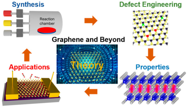
This review reflects the content of the 2021 Graphene and Beyond workshop hosted at the Pennsylvania State University, in which a diverse group of experts discussed recent advances in the field of 2D materials from both theoretical and experimental perspectives. As summarized in Figure 1, we first highlight recent progress in theory-guided synthesis including substrate-directed growth, liquid exfoliation, metal–organic chemical vapor deposition (MOCVD), and confinement heteroepitaxy (CHet) of 2D materials. Subsequently, we review methods for engineering atomic defects in these materials including in situ and ex situ methods. Next, the review focuses on properties including magnetism, topological properties, photonics, and moiré engineering of 2D materials. Finally, we discuss emergent applications discussed during the conference including 2D electronics, sensors, strain engineering, and 2D artificial intelligence (AI).
Figure 1.

Overview of the scope of this paper. Focusing on the recent advancements in the field of 2D materials, we discuss theory guided synthesis via different approaches, engineering of atomic defects, study of emergent properties, and the development of devices for functional applications. Adapted with permission from ref (4). Copyright 2020 Springer Nature.
1. Theory Guided Synthesis
As the field advances, one must consider large-scale synthesis of 2D materials that possess desired properties, with improved control over their morphology, degree of crystallinity, and layer numbers via bottom-up or top-down approaches. In this case, it is prudent to explore theoretical and experimental endeavors to achieve this goal. On one hand, calculations and theory predictions are performed to provide guidelines for developing novel 2D materials with potentially high mobility and to evaluate 2D material integration with complementary metal oxide semiconductor (CMOS) processes. On the other hand, experimental studies are carried out to investigate epitaxial growth for large-area, single-crystalline films, morphological control, and methods to develop novel 2D materials unattainable by standard material synthesis. In this section, we review some of these recent advances in the synthesis of 2D materials.
1.1. Theory Guidelines for Predicting/Screening High-Mobility 2D Materials
Carrier mobility characterizes the average velocity of carriers (electrons/holes) moving through a material in the presence of an electric field. In this case, a high carrier mobility is desired for most electronic and optoelectronic applications. The room-temperature mobility of current 2D monolayer semiconductors is on the order of ∼10–1–102 cm2 V–1 s–1,10,11 whereas the electron mobilities of bulk Si, Ge, and InAs are ∼1400, 3900, and 33000 cm2 V–1 s–1,12,13 respectively. As a result, it is crucial to understand what limits the carrier mobility in 2D semiconductors and develop guidelines in the search for novel high-mobility 2D materials.
In a recent work, Liu et al. demonstrate that this limitation is largely due to effects resulting from the dimensionality.14 Using first-principles calculations to study the intrinsic mobility of various monolayer 2D semiconductors, and reformulating the transport equations to isolate and quantify contributions of different mobility-determining factors, it is found that the low electron mobility originates from a high density of electron–phonon interactions (scatterings) that naturally occur even in perfect 2D semiconductors. Adopting a “density of scatterings” concept leads to simple guidelines in the search for high-mobility 2D semiconductors: one should look for a single, deep, and sharp valley in electronic structure,14 a high phonon frequency, and/or a high sound velocity.15 These properties can help reduce the density of scatterings. Moreover, for some polar 2D semiconductors such as HfS2, in addition to the density of scatterings, another factor that limits the mobility is the strong interaction between carriers and longitudinal optical (LO) phonons, as a result of large Born effective charge and poor screening.16 Thus, one should also avoid strongly polar materials in the search for a high-mobility 2D semiconductor.
1.2. Theory-Guided Understanding of TMD Reactivity
The semiconducting properties of TMDs enable the scaling of CMOS to dimensions which would not be attainable with silicon technology. However, several roadblocks exist that prevent these materials from reaching their full potential including: difficulties in maintaining their high mobility (see previous section);17 the occurrence of intrinsic defects; adhesion issues; and their sensitivity to the different integration steps, such as integrating with metals to form ohmic contacts,8,18 the building blocks of a transistor. Therefore, gaining an understanding of the chemical reactivity of TMDs is key to their engineering.
The evaluation of the thermodynamic driving forces of chemical reactions using first-principles simulations is a convenient approach that allows linking the material evolution occurring through the growth, the deposition of a dielectric, their doping, etc., while accounting for the role of grains, defects, impurities, and device processing conditions. In this context, a thermodynamic database was computed, including more than 250 W and Mo volatile and solid sulfides related derivatives, including molecules, cluster prototypes, flakes (with lateral dimensions up to 6 nm), multiple sources of interstitial impurities (C, N, O, etc.), and a broad range of thermal and pressure conditions, going from 10–9 to 100 Torr, to account for different possible processing conditions. MOCVD is a highly scalable process used for the growth of TMDs on a variety of substrates.19 This deposition method is a high-pressure (1–700 Torr) synthesis process, and in many cases, it relies on the reaction between, for example, M(CO)6 (M = W, Mo) and H2S, in a thermal window that spans from 400 to 1000 °C. Since carrier gases such as H2, N2, and Ar are typically used,20,21 the total pressure present within the reactor does not necessarily reflect the partial pressure of the reactants which, in some instances, can be extremely low (e.g., 10–9 Torr). As an attempt to capture the impact of a distribution of grain dimensions22 on their stability during the growth, the evolution of the equilibrium composition during the growth of three equilateral triangular-shaped grains with dimensions spanning from 2.2 to 6.0 nm (Figure 2a) was simulated. It was observed that, depending on their size, the MoS2 grains tend to undergo a self-etching process that releases gaseous MoS3 with a critical temperature that increases with their size, going from 700 °C (2.2 nm) to 1000 °C (for large systems). The growth process is modulated with the reactor pressure as illustrated by the ∼250 °C variation obtained when going from 10–9 to 100 Torr (Figure 2b). This effect is attributed to the difference in the formation energies of S vacancies (ΔHf) that vary from the middle to the edge of the grains as a function of the base size (Figure 2a inset). While ΔHf of the “middle grain” S vacancies shows a minimal dependency on the grain size, the one computed at the edge of the grain is significantly lowered and increases gradually with the size of the grain due to the difference in atomic coordination. S vacancies, being more prominent on the edges, act as etching/reactive centers for the flakes as observed in ref (23). In a MOCVD process, the reactor pressure and the nature of the carrier gas used drives the size of the grains due to the modulation of the sublimation/etching temperature.
Figure 2.

Thermodynamic computation for MoS2 synthesis at various temperatures. (a) Comparison of the equilibrium composition of different grain size models for MoS2 at 1 × 10⁻⁹ Torr. An initial molar ratio of 100:1 is used for H2S and Mo(CO)6. The ordinate corresponds to the number of moles of different reactants and products present in the reaction chamber. The different MoS2 grain sizes are shown in color with their corresponding base lengths in nm, and byproducts are colored in gray; inset, evolution of the S vacancy formation energies (ΔHf) for different MoS2 grain sizes going from 2.2 nm to an ideal monolayer (1 ML). The blue circles depict the formation energies corresponding to the edge S vacancy, and the red circles represent the formation energies of the middle S vacancies. (b) Evolution of the equilibrium composition of different grain size models.
1.3. Large Area Growth by MOCVD: The Case of WS2
MOCVD is a standard semiconductor synthesis process and also a promising technique for scalable synthesis of TMD monolayer films on wafers.19,24,25 It also provides the flexibility to control the source partial pressure independently during growth. Compared to solid source or powder-based CVD (ssCVD or P-CVD) widely used for the synthesis of TMD monolayer domains, MOCVD can operate at temperatures lower than ssCVD and still deliver appreciable metal source flux. Figure 3a provides an illustration of a MOCVD system in a cold-wall reactor geometry for TMD synthesis.26 The substrates for film deposition are placed on the graphite susceptor, which is heated to high temperature by the radiofrequency (RF) induction coil. The substrate is constantly spinning at a constant rate during deposition to achieve good film uniformity over the inch-size area. The MOCVD system utilizes volatile precursors and gaseous molecules to deposit WS2, MoS2, and other TMD films.27 W(CO)6 stored in a bubbler is delivered into the reactor by regulating the carrier gas flow and bubbler pressure with the mass flow and pressure controller. H2S gas is also used to supply sulfur. C-Plane sapphire ((0001) α-Al2O3) not only has good thermal and chemical stability but also exhibits crystallographic compatibility with TMDs. The lattice mismatch between WS2 and sapphire (30%) can be reduced significantly by the formation of domain epitaxy (i.e., 3 unit-cells of WS2 match with 2 unit-cells of α-Al2O3). Therefore, it is a promising substrate for the epitaxial growth of WS2 at high temperatures.
Figure 3.

Wafer scale synthesis of epitaxial 2D WS2 by MOCVD. (a) Illustration of a MOCVD system (left) and close view of reactor (right) used for the growth of WS2 monolayer films. (b) Illustration of precursor and carrier gas flow rates and substrate temperatures during the multistep process at variable temperature. (c) AFM image of WS2 monolayer grown at 1000 °C for 10 min when nucleation and ripening were carried out at 850 °C. (d) Schematic shows that well-aligned domains oriented by the substrate step edges are observed when the surface step structure is modified less by performing the nucleating and ripening stages at 850 °C. (e) Isolated WS2 domains obtained at a constant-temperature process at 1000 °C. (f) High-temperature exposure starting at the beginning of the process distorts the surface step structure, resulting in WS2 domains nucleating in various orientations. (g) Photograph of a WS2 monolayer film grown on a 2 in. sapphire using the multistep process described in (b). (h) AFM image of films deposited at a growth rate of 3 monolayer/min shows a continuous monolayer (1L) with a small amount of bilayer domains. (i) In-plane XRD φ-scans of the (1010) and (3030) planes of WS2 and sapphire, respectively, show the coincidence of their peak positions, indicating that the film/substrate relationship is epitaxial. (j) High-resolution Z-contrast STEM image shows that two domains with the same orientation are separated by a line defect caused by the translational offset between the two domains. Their same orientation is highlighted by the WS2 models superimposed on the image. Adapted from ref (26). Copyright 2021 American Chemical Society.
In order to reduce high-angle grain boundaries caused by misoriented WS2 domains and the inversion domain boundaries (IDB) that form between coalesced 0° and 60° domains, Choudhury et al. reported a multistep MOCVD process for WS2 that etches and modifies sapphire steps to orient all WS2 nuclei at the same direction (Figure 3b).26 In this process, the nucleation step of WS2 with a high W(CO)6 flow is carried out at a lower temperature of 850 °C. After the nucleation step, the deposited nuclei on sapphire are heated to 1000 °C at the ripening step without a W(CO)6 flow to minimize H2-induced sapphire surface roughening. After these early steps, a smaller flow of W(CO)6 is reintroduced to grow WS2 nuclei into larger domains and ultimately to form a continuous monolayer film. The multistep WS2 synthesis recipe can regulate domain orientation such that the zigzag edge of each domain is parallel to the straight sapphire step edge (Figure 3c,d).26 A high density of epitaxial WS2 domains from this process that orient at the same direction is also observed in the AFM image, which can help reduce the density of IDB in a continuous WS2 film. On the other hand, if the early stages for both WS2 nucleation and ripening are conducted at 1000 °C, the etching of sapphire steps can proceed at a faster rate than nuclei formation and growth, leading to misoriented WS2 domains along curved sapphire steps (Figure 3e,f).26 By following this recipe, a 2 in., fully coalesced, WS2 monolayer film (Figure 3g) with an atomically flat surface (Figure 3h) can be achieved. Additionally, the growth rate is controlled at 3 layers/hour to minimize bilayer coverage. In-plane X-ray diffraction (XRD) Phi scans of (1010) and (3030) planes of WS2 and sapphire, respectively, reveal the coincidence of the WS2 peak positions with sapphire peak positions, indicating that (1010) WS2 is parallel to (100) sapphire (Figure 3i).26 A dark-field STEM image shows that two WS2 domains are unidirectional but separated by a line defect due to translational offset between the two domains (Figure 3j). Therefore, to push film quality to electronic grade, each domain needs to grow larger to minimize the density of such line defects in continuous films induced by the translational offset.
1.4. Patterned Growth/Substrate Mediated Growth
The morphology and dimensionality of 2D crystals determine many of their key physical properties.28 Recent work on the synthesis of graphene and TMD nanoribbons29−34 has been motivated by an interest in constraining the dimensionality of 2D crystals toward the 1D limit to realize a tunable bandgap,35,36 enhanced thermoelectric performance,37 ferromagnetism,38 width-dependent phase stability,39 and spatially heterogeneous electronic properties.30 However, while many intriguing material properties are dictated by crystal morphology and dimensionality, synthetic control of a 2D crystal’s size, shape, phase, and layer number is still a major hurdle. Typically, bulk and 2D TMDs are prepared by CVD during which TMD precursors undergo surface adsorption, surface diffusion, and bond formation/rearrangement to yield a planar 2D crystal lattice.40−45 Top-down fabrication methods are frequently used to pattern raw crystals, but these methods involve lithography and etching processes that present some challenges, namely, intrinsic resolution limits which complicate efforts to tune materials to atom-levels of precision, and etch processes which can damage 2D crystals. A number of approaches to prepare dimensionally restricted forms of graphene and 2D TMDs include molecular beam epitaxy,30 ledge-directed epitaxy,32 CVD growth through vapor–liquid–solid processes,31,33 and highly anisotropic growth by CVD on Ge(001) substrates.34,46
Recently, rational strategies have been demonstrated for controlling the dimensionality of 2D TMD crystals. It was shown that synthetic surfaces, in this case Si substrates pretreated with phosphine (PH3), can precisely control the lateral growth of TMD crystals. ssCVD synthesis of MoS2 on Si(001) surfaces functionalized with phosphine yields high aspect ratio and straight nanoribbons which have uniform widths.29 Notably, the width of these nanoribbons is systematically controllable between 50 and 500 nm through adjustment of the phosphine partial pressure during the Si surface treatment process (Figure 4a). It is also notable that this gas-phase method can significantly transform the dimensionality (i.e., from 2D to nominally 1D) of TMD crystals without the use of pattern and etch processes, which as discussed above have their attendant limitations. Aberration-corrected scanning transmission electron microscopy (STEM) reveals that the nanoribbons are crystalline (predominantly of the 2H phase) and exhibit an excellent edge sharpness and uniformity that rivals that found in most graphene and TMD nanoribbons prepared through conventional fabrication routes (Figure 4b). Because of their restricted dimensionality, the MoS2 nanoribbons exhibit photoluminescence which is 50 meV higher in energy than that emitted from 2D MoS2 crystals. This emission is dependent on the crystal width, which is synthetically tunable (Figure 4c). Cluster expansion and density functional theory (DFT) calculations suggest that the nanoribbons preferentially nucleate within regions of the substrate coated with Si–P surface dimers. Meanwhile, inhibition of lateral growth in the direction of the regions coated with P–P surface dimers manifests as heterogeneous nucleation of the MoS2 nanoribbon nuclei to yield crystal growth which is laterally restricted in one direction (Figure 4d).
Figure 4.

Substrate-mediated control of TMD nanocrystal growth. (a) Average widths (wmean) for randomly sampled MoS2 nanoribbons grown on surfaces treated with the indicated PH3 dosages (VPH3). SEM of a single nanoribbon. Scale bar: 500 nm. (b) HAADF-STEM images of the interior and edge of a MoS2 nanoribbon. Scale bars: 5 Å (top), 2 nm (bottom). (c) PL spectra (left) from the indicated regions of a MoS2 nanoribbon with tapered width. Scale bar: 1 μm. (d) SEM image of the early stage of MoS2 nanoribbon growth and corresponding schematic. Scale bar: 500 nm. Adapted from ref (29). Copyright 2020 Springer Nature.
1.5. Confinement Heteroepitaxy
Confinement is also advantageous for developing novel low-dimensional materials. Reducing the material dimensions from 3D to 2D can lead to band structure renormalization and novel material properties because of quantum confinement.47−49 While hexagonal boron nitride (hBN), graphene, and TMD monolayers are excellent examples of insulating, semimetallic, and semiconducting layered materials in the 2D limit, the synthesis and properties of 2D metals remain nebulous. Metals rarely exist in layer form, and most of their surfaces rapidly oxidize in ambient conditions.50,51 This means that making ultrathin metals without structural and chemical degradation is difficult outside of an inert environment. Intercalation enables the decoupling of surface layers from the rest of bulk body or substrates and serves to stabilize atomic species that are sensitive in ambient conditions. Both epitaxial graphene (EG) and carbon buffer layer grown on SiC can be physically and electronically decoupled from the SiC by intercalating atomic species, such as F, O, H, Ge, and Li, to their interface.52,53 The intercalation with metal had not been explored extensively except for a few demonstrations with transition metals such as Pd, Au, and Cu.52 Recently, 2D forms of Ga, In, Sn, Cu, Bi, Pb, and Ag confined between EG and SiC were made possible by CHet.4,54Figure 5a illustrates the CHet method for 2D metal synthesis at the EG/SiC interface. First, SiC (0001) is annealed at high temperature to sublime Si atoms and leave C atoms on the surface to recrystallize into a carbon-rich layer (the buffer layer) partially bound to SiC. Further annealing leads to continued Si-sublimation, and this first layer fully detaches from the SiC, while a second layer, underneath the first, forms the next buffer layer (Figure 5a). Second, EG/SiC is treated with an O2/He plasma to generate vacancies that serve as the entry for intercalated elements. Finally, metal precursor atoms placed in a crucible beneath the plasma-treated EG are annealed with the EG/SiC at 700–1000 °C at 300–700 Torr to vaporize the metal onto the graphene surface, which subsequently diffuse through the EG defects to reach the EG/SiC interface. After intercalation, Z-contrast STEM reveals that 2D metals (e.g., Ga) release the buffer layer and exhibit an asymmetric bonding environment at the interface. They are covalently bonded to SiC at the bottom, whereas their top surface adjacent to the released buffer layer only has van der Waals (vdW) bonds.
Figure 5.

CHet with defect-engineered epitaxial graphene/SiC. (a) Schematic representation of CHet and the resulting atomic structure of the 2D metals (using Ga as the prototypical example) formed via CHet. (b) DFT study of interactions between a Ga atom and unpassivated and passivated defects of graphene suggests that graphene defects passivated with oxygen termination facilitate metal diffusion through the graphene sheet. The binding energy of a Ga atom to each defect is shown in each model. (c) SEM images and corresponding Ga AES maps of as-grown EG with intercalated Ga (top row) and O2/He plasma-treated EG with intercalated Ga (bottom row). Defects formed on EG due to O2/He plasma treatment can improve intercalation uniformity significantly. The AES color scales show low (dark) to high (light) Ga signal across the map. (d) Atomic structure of CHet-grown 2D In and Sn metals with two and one atomic layer, respectively. LEED pattern for EG/Ga/SiC indicating the presence of EG and SiC with no additional spots, implying the Ga is lattice matched to top EG or bottom SiC. (f) (Left) DFT-generated, top-down schematic of hexagonal SiC with silicon, carbon, and hollow sites labeled. (Right) Side view of DFT-predicted model shows intercalated Ga layers exhibit an ABC stacking over the SiC substrate. Adapted with permission from ref (4). Copyright 2020 Springer Nature.
The C–O bonding previously detected by X-ray photoemission spectroscopy (XPS) and the defect-induced Raman characteristic peak of graphene (D peak) in O2 plasma-treated EG disappear after intercalation, indicating the EG heals at elevated temperature in the presence of the metal intercalant and becomes an oxidation barrier that improves the sample air stability. These O-related functional groups are not trivial but play an important role. The energetics based on first-principles calculations suggest that termination of graphene vacancy with O atoms and OH groups can facilitate metal adhesion and transport to the EG/SiC interface prior to EG healing. Otherwise, the metals could have passivated these graphene vacancies and blocked the intercalating channels because C–Ga binding energy appears to be several eV higher than those between Ga and a few C–O terminations (Figure 5b).4 Auger electron spectroscopy results of EG/Ga samples on pristine vs plasma-treated EG reveal that the plasma treatment is the key to achieve a high lateral surface coverage of intercalated Ga (Figure 5c).4 The 2D metals are found to generally be 1–3 atomic layers thick (Figure 5d) based on equilibrium phase stabilities relative to their own bulk 3D form. The successful intercalation of most elements suggests that they react with graphene defects created at the early stage of CHet in a similar way and follow similar transport kinetics during the intercalation, due to similar elemental properties. Low-energy electron diffraction of EG/SiC patterns does not include any distinct spots that belong to inserted 2D metal layers. Since the Ga lateral spacing observed by STEM closely matches the spacing of SiC, it was determined that SiC and Ga share the same diffraction pattern in LEED, thereby having an epitaxial relationship (Figure 5e).4 The structural optimization based on first-principle calculations provides the top and side views of epitaxial Ga/SiC (001) (Figure 5f).4
1.6. Liquid Exfoliation
Other than the bottom-up approaches mentioned above, the liquid phase exfoliation (LPE) of layered crystals such as graphite and TMDs is a scalable top-down method to produce novel 2D nanosheet based inks such as graphene and ultrathin 2D TMDs.55 The layered crystal starting materials are stacked by vdW forces; hence, it is necessary to peel them apart without introducing significant structural defects on the lattice of the 2D nanosheet. Mechanical exfoliation using the Scotch-tape method yields the highest-quality monolayered 2D samples, which are ideal for demonstration of high-performance devices and condensed-matter phenomena.56 On the other hand, the liquid-phase exfoliation has the advantages of producing 2D materials in bulk quantities, with fairly good crystalline quality that suits most applications at an affordable price to industry.1 The manipulation of 2D materials in the liquid phase enables their chemical functionalization which can improve their functionality.57 These 2D nanosheet based inks can be easily processed and can be adapted for many thin film membranes and device fabrication techniques.6,58 However, the 2D nanosheets produced using the LPE still face some significant disadvantages.
First, the use of ultrasonication and high shear mixing in the LPE often introduces structural defects in the lattice of the 2D nanosheets.59 Defect healing by chemical functionalization in LPE processed 2D nanosheets could be a viable strategy for producing high performing 2D nanosheets in thin film devices. For example, recent studies have shown that sulfur vacancy defects in TMD nanosheets of the form MS2 could be healed by reacting the TMD inks with 1,4-benzenedithiol.60 The opposite ends of the 1,4-benzenedithiol react with different MS2 flakes and, as a result, act as a covalent bridge between adjacent flakes. This approach can be applied to thin films by exposing them to such molecular linkers as indicated in the scheme in Figure 6a, resulting in the formation of long-range pathways in 2D nanosheet films that exhibit superior charge-transport characteristics. Second, the use of ultrasonication and high shear mixing in the LPE of bulk layered crystals produces 2D nanosheets with a broad thickness distribution, which makes it hard to assess exfoliation quality and limits the suitability of the 2D nanosheets for applications. The chemical intercalation followed by dispersion of layered crystals is an effective method of preparing additive-free, ultrathin, and uniform dispersions of 2D nanosheets, in low-boiling-point solvents.61−63 High quality thin film-based devices can be fabricated from the deposition of 2D nanosheet based inks prepared using the redox driven intercalation and dispersion of layered materials.6 Third, the use of stabilizing agents and high-boiling-point solvents to assist in the LPE usually results in the trapping of these substances between the 2D nanosheets, thus inhibiting strong interlayer coupling in thin films.6 To achieve compact stacking postdeposition, ultrathin, uniform, and additive-free 2D nanosheet dispersions in low-boiling-point solvents are required. The chemical intercalation followed by dispersion of layered crystals is an effective method of preparing additive-free, ultrathin, and uniform dispersions of 2D nanosheets, in low-boiling-point solvents.61−63
Figure 6.

LPE of vdW and non-vdW materials. (a) Schematic of S-vacancy healing mechanism in MoS2 films by means of dithiolated molecules and related interflake networking. Adapted with permission from ref (60). Copyright 2021 Springer Nature. (b) Pyrite exfoliation process, showing photographs of pyrite mineral, crushed mineral before and after cleaning treatment, and exfoliated pyrite dispersion obtained after liquid-phase exfoliation process. Adapted with pemission from ref (65). Copyright 2021 American Chemical Society. (c) Top left: bright-field TEM image of a single sheet. Scale bar, 0.5 μm. Top right: high-magnification bright-field TEM image of a monolayer and bilayer hematene. Scale bar, 50 nm. Bottom: HRSTEM image of hematene in the (001) orientation with its Fourier transform in the inset and position of atoms shown by red (O) and yellow (Fe) spheres. (d) Planar and cross-sectional simulated view of the hematene (001)-oriented plane.64 Adapted with permission from ref (64). Copyright 2018 Springer Nature.
More recently, the LPE technique has been utilized to produce new and exotic non-vdW 2D nanosheet based inks by exfoliating nonlayered materials such as earth abundant chemical compounds composed of iron and sulfur or oxygen (Figure 6b).65 For example, the sonication-aided LPE of the abundantly occurring minerals, hematite (α-Fe2O3)64 and pyrite (FeS2),65 yielded new 2D materials, ultrathin hematite (hematene) and ultrathin FeS2 inks, respectively (Figure 6b). The exfoliation and formation of mono- and bilayer hematene structures were confirmed by HRTEM (Figure 6c,d). The exfoliated 2D α-Fe2O3 materials exhibit ferromagnetic order, as opposed to the bulk form which exhibits antiferromagnetic order. The exfoliated 2D Fe2S flakes exhibit anomalous ferromagnetic-like behavior different from their diamagnetic bulk counterparts. The 2D Fe2S platelets were also used to produce Li-ion battery anodes with excellent capacities approaching 1000 mAh/g.66,67
2. Defect Engineering
The manipulation of defects in 2D material presents important opportunities for fine levels of material property control. 2D materials can possess a variety of structural defects with dimensions ranging from 0D (e.g., vacancy, adatom, and dopant) to 2D (e.g., layer stacking faults), which significantly influence their physicochemical properties.8 As a result, if the density and specificity of these defects can be controlled and the properties of certain defects understood, defect engineering can be realized for tuning properties and/or inducing new functionalities into 2D materials. With 0D point defects taken as an example, routes for engineering them in 2D materials can be classified into two categories: (1) in situ approaches which directly introduce or minimize defects during the growth process; and (2) ex situ approaches which are based on post-synthesis treatments that create or heal point defects. Because of the great significance of developing robust techniques for engineering defects in 2D materials, many efforts have been made along this direction in recent years. In this section, we will highlight recent advancements regarding approaches for in situ and ex situ defect engineering of 2D materials.
2.1. In Situ Substitutional Doping/Alloying of 2D Materials
Early work on in situ substitutional doping of TMD monolayers utilized a two-step approach, in which chemical vapor transport (CVT) was first used to synthesize doped TMD single crystals, and monolayers were then isolated from these single crystals by mechanical exfoliation. This method has been reported to yield TMDs doped with Nb, Re, Au, etc.68,69 To improve the yield and simplify the preparation of monolayers, CVD using mixed metal precursor powders was then developed to synthesize doped TMDs in a single step.70,71 Recently, an alternative in situ doping approach has been devised, which relies on the chalcogenization of mixed liquid-phase metal precursors coated on the growth substrate (i.e., liquid-phase precursor-assisted approach). Since metal precursors are uniformly mixed at the atomic level in the liquid phase and spin-coated onto the growth substrate prior to the chalcogenization process, this method circumvents the difficulty of controlling vapor pressures of both host and dopant precursors to enable effective doping. As a result, by using a liquid-phase precursor-assisted doping approach, it is likely that the spatial variation of precursor supply can be reduced, leading to improved spatial homogeneity of dopant distribution when compared to the conventional CVD using powdered metal precursors.72,73
In a recent work by Zhang et al., liquid-phase precursor-assisted in situ substitutional doping of Fe, Re, and V into monolayer WS2, MoS2, and WxMo1–xS2 – MoxW1–xS2 in-plane heterostructures, respectively, was achieved. The flow diagram describing the substitutional doping process is shown in Figure 7a. First, water-soluble ammonium heptamolybdate ((NH4)6Mo7O24) and ammonium metatungstate ((NH4)6H2W12O40) were used as Mo and W precursors, which were mixed in the aqueous solution with sodium cholate (C24H39NaO5·xH2O, serving as a growth promoter) and the water-soluble compound containing the desired dopant element. Subsequently, the mixed solution was spin-coated onto a clean SiO2/Si wafer, followed by a sulfurization process carried out at 800 °C inside a tube furnace. To verify the incorporation of Fe, Re, and V dopants, the synthesized doped monolayers were characterized using atomic-resolution STEM. As an example, the schematic of V-doped WxMo1–xS2 – MoxW1–xS2 in-plane heterostructures and corresponding high-angle annular dark field (HAADF)-STEM images from center (Mo-rich) and edge (W-rich) regions are demonstrated in Figure 7b–d. Based on the atomic Z-number differences, V dopants, Mo, and W are unambiguously identified in both images (Figure 7c,d) according to their increasingly brighter contrasts, indicating the successful incorporation of V dopants into the host lattice.72 Similar liquid-phase precursor-assisted methods have also been developed to obtain different types of doped TMD monolayers. For example, Nb-doped WS2 was synthesized and characterized, demonstrating tunable optical properties and p-type transport characteristics as a function of doping level.73 V-doped MoS2, WS2, and WSe2 synthesized via similar methods were also reported by a number of separate studies. Intriguingly, apart from V dopants-induced modification of optical and electronic properties, room-temperature ferromagnetic ordering was also observed in these systems.74−77 These recent studies indicate that this doping approach is efficient, reliable, and highly likely to be generalized for the incorporation of other metal dopants that are not yet explored.
Figure 7.

In situ substitutional doping and alloying of 2D materials and heterostructures. (a) Flow diagram of the liquid-phase precursor-assisted substitutional doping approach. (b) Schematic illustration of V-doped in-plane WxMo1–xS2 – MoxW1–xS2 heterostructures. (c,d) Atomic-resolution HAADF-STEM images from center and edge regions of the V-doped WxMo1–xS2 – MoxW1–xS2 heterostructures. Examples of Mo, W, and V atoms are marked with red, green, and blue circles, respectively. Adapted from ref (72). Copyright 2020 American Chemical Society. (e) The composition of the 2D-InxGa1–x alloys can be tuned by adjusting the precursor composition, with a near linear relationship between alloy and precursor compositions. (f) Ga and In AES maps of the 2D-In 0.5Ga0.5 alloy shows uniform distribution of Ga and In across the map. (g) Atomic structure of the 2D-InxGa1–x alloys and accompanying EELS mapping show a uniform 2D-In0.5Ga0.5 alloy bilayer confined between EG and SiC. Adapted with permission from ref (82). Copyright 2020 John Wiley & Sons, Inc.
Doping TMD atomic layers by MOCVD has also advanced significantly and can control the doping range at the parts per million (ppm) level inside a grown 2D crystal.78,79 Kozhakhmetov et al. demonstrates controllable doping of V and Re originally from (C5H5)2V and Re2(CO)10, respectively, into WSe2 monolayers during MOCVD.78,79 Re2(CO)10 which provides Re is delivered into the MOCVD chamber through the bubbler manifolds by H2 carrier gas flow rate. By reducing the flow rate through the bubbler manifold for Re2(CO)10, 0.07% Re in WSe2 monolayer can be achieved. It is essential to control the doping concentration on the ppm level for bilayer, trilayer, or thicker TMD crystals, since their electronic properties are more sensitive to the density of dopants because the quantum confinement effect becomes less significant on thicker TMD.80,81 Excessive dopants can degrade the electronic transport of a few-layer TMD device in comparison with the field-effect transistor (FET) made of 1L TMDs.80
Beyond TMDs, in situ alloying is also possible in 2D metals. By alloying the composition of 2D metals, the interband contributions to dielectric properties, Fermi surface geometry dependent on alloy composition, and both optical and electrical response could be possibly tuned. Rajabpour et al. reported the synthesis and characterization of 2D-InxGa1–x via CHet discussed in Section 1.5, and achieved near-complete solid solubility without evidence of phase segregation.82 XPS measurement performed on 2D-InxGa1–x with varying composition reveals a nearly linear correlation between the composition of the InxGa1–x precursors and the resulting stoichiometry of the 2D metal alloys, indicating the full range of x between 0 and 1 can be achieved by tuning the precursor compositions (Figure 7e). Additionally, Auger electron spectroscopy (AES) mapping reveals that intercalated 2D alloys are uniformly distributed without evident in-plane segregation, as evidenced by the uniform spectral intensity of Ga and In across the mapped area (Figure 7f).82 This unform dispersion of Ga and In inside the 2D alloy was also confirmed by Z-contrast STEM image of a 2D In0.5Ga0.5 bilayer film at the EG/SiC. Electron energy-loss spectroscopy (EELS) mapping indicates a unform distribution of Ga-L2,3 and In-M4,5 EELS signals within the bilayer without oxygen, and the ratio of Ga/In close to 1 (Figure 7g).82
2.2. Plasma-Assisted Carbon–Hydrogen (CH) Doping of Monolayer TMDs
Atomic dopants can also be substitutionally incorporated into 2D TMDs via post-synthetic treatments. In a recent work, a plasma-assisted approach was applied to achieve C doping in monolayer WS2. During the doping process, an inductively coupled plasma was used to decompose methane (CH4), the gaseous dopant precursor, into reactive radicals (possibly carbon and hydrocarbons), which were likely to be incorporated into the lattice of as-grown WS2 through sulfur vacancies. Through aberration corrected high-resolution STEM (AC-HRSTEM) in combination with DFT calculations, it was identified that carbon–hydrogen units at sulfur sites (CHS) are the most stable dopant structure within WS2. Interestingly, electronic transport measurements of CH-doped monolayer WS2 reveal the emergence of p-branch that is tunable by varying CH doping concentrations, demonstrating that CH units can effectively modulate electronic properties of 2D TMDs.83 Plasma-assisted CH doping was further performed on WS2 grown on EG/SiC substrate, and scanning tunneling microscopy and spectroscopy (STM/S) were employed to further characterize CHS defect properties. The CHS defect is negatively charged detected by a significant upward band bending in the unoccupied states (positive sample bias) and the presence of hydrogenic bound states in the occupied spectrum (at negative bias).84,85 Notably, such negatively charged defects were also observed by STM/S in as-grown pristine WS2 and WSe2 samples, which unambiguously indicates that CH units at chalcogen sites are a common type of charged impurity in nominally undoped CVD-grown TMDs. This work not only corroborated the previous finding that CH4 plasma-assisted approach could selectively introduce CH units into TMDs, but also demonstrated STM/S as a powerful tool to characterize atomic defects in 2D materials.85
2.3. STM Tip-Induced Creation of Carbon Radical Ion (CRI) in Monolayer WS2 and Its Vibronic Properties
Atomic manipulation using the STM tip is a novel route to defect engineering of 2D materials. This technique has previously been used to create complex patterns on surfaces using adatoms.86 Lateral manipulation relies on weak forces between the tip and sample to pull or push atoms around. In covalently bonded materials, this is extremely difficult to realize, given their significantly higher bond strengths. Alternatively, voltage pulses from the STM tip can be used to break weak bonds. Thereby electrons are injected at a comparably high energy of usually a few eV, which can transiently populate antibonding orbitals and excite lattice vibrations that lead to bond cleavage.87 Typical examples of tip-induced bond dissociation include hydrogen–carbon and halogen–carbon bonds in organic molecules.20−22 In solid-state systems, voltage pulses can desorb individual hydrogen atoms from a hydrogen-terminated silicon surface.87−89 This so-called hydrogen resist lithography can be used, for instance, to build single-atom transistors.90
By a chemical methane plasma treatment of the TMD surface described in the preceding section, it is possible to introduce CHS defects in the TMD lattice. Using a scanning probe tip, one can apply a local voltage pulse to desorb hydrogen from an individual CH-dopant in monolayer WS2. This process exposes the dangling bond of the carbon atom remaining at the sulfur site.91 Thereby, the STM contrast at positive bias changes from a circular dark depression to a bright threefold symmetric protrusion superimposed on the dark depression (see Figure 8a). The hydrogen depassivation process is highly selective and can be targeted at a single defect.91 After hydrogen depassivation, the defect exhibits two in-gap resonances in scanning tunneling spectroscopy (STS), one at positive and one negative bias (see Figure 8b). These defect resonances correspond to the electron attachment/detachment from a singly occupied orbital. Because it is singly occupied and the defect still carries a negative net charge, this defect can be denoted as a carbon radical ion (CRI) or CS•–. DFT calculations show that the CRI has a spin-polarized ground state (see Figure 8c) with a magnetic moment of 1 μB.91 Despite the rather directional bonding, the magneto crystalline anisotropy energy is only 0.3 meV with an easy-axis perpendicular to the WS2 plane.
Figure 8.

Creating the CRI in WS2 by tip-induced hydrogen-depassivation from CHS. (a) STM images (V = 1.1 V, I = 100 pA) after sequential H desorption using 2.5 V and 15 nA. (b) Constant height dI/dV measurement across CHS in monolayer WS2 before (left) and after (right) H dissociation. Both CHS and CS are negatively charged. The half-occupied dangling bond state of the CRI appears as two resonances in the band gap at positive and negative bias in (left). (c) Calculated band structure of the negatively charged CHS and CS, respectively. (d) Vibronic excitations associated with charge state transitions of CRI. Electron/hole attachment to the unoccupied/occupied defect state in monolayer (1 ML) and bilayer (2 ML) WS2, respectively. Adapted with permission under a Creative Commons CC-BY License from ref (91). Copyright 2021 Springer Nature.
The defect resonances exhibit a striking oscillatory fine-structure with equidistant peaks, as seen in Figure 8d. One can assign these peaks to inelastic excitations of local lattice vibrations in response to the transient electron/hole attachment process. The vibronic satellite peaks can be modeled by considering the electron–phonon coupling between the electronic defect state and a small number of local vibrational modes. Using density functional perturbation theory, three contributing modes are identified at ℏω = 75 meV, ℏω = 22 meV, and ℏω = 5 meV, corresponding to a local out-of-plane C vibration, an out-of-phase breathing motion involving the C–S bond and the neighboring three W atoms, and a low-frequency resonant flexural mode.7 The difference in coupling strengths to these modes is what ultimately gives rise to the very different sideband structure shown in Figure 8d.
Interestingly, the electron–phonon coupling strengths described by the Huang–Rhys factors Sω critically depend on the spin state (cf. left column vs. right column in Figure 8d). The considerable spin–phonon coupling originates not only from differences in the exchange-correlation potential that depends explicitly on spin density but also from small differences in the charge density distributions.91 The coupling to a certain vibrational mode is in general stronger if the wave function of the defect state is more localized at the lattice sites where the vibration occurs. Moreover, it is observed that the vibronic coupling is in general stronger for monolayer WS2 as compared to bilayer WS2 (cf. top row vs. bottom row in Figure 8d), because the defect wave function in the bilayer spreads across both layers, reducing the degree of localization. This first demonstration of atomic editing of the TMD surface via STM-induced hydrogen depassivation opens new avenues for defect engineering of 2D semiconductors.
2.4. Defect Control by MOCVD
As stated above, MOCVD utilizes chemical compounds with low to moderate vapor pressure and gases as precursors for large-scale TMD synthesis.45 It provides a wide window of growth pressures and growth temperatures and can be conducted in an intermediate growth regime that off-limits to other thin film methods (Figure 9a).92 For example, in the low-temperature regime below 600 °C (Figure 9b), TMD domains and defect density synthesized by MOCVD are more tunable than those from atomic layer deposition (ALD) and molecular beam epitaxy (MBE).92 The precursor ratios between chalcogen and transition metals are controllable during MOCVD and can be tuned to provide a chalcogen-rich or -poor environment to form or suppress the point defects in the resulting TMD films.19,24,93
Figure 9.

In situ defect control for 2D TMD during MOCVD. (a,b) Operation windows of common scalable synthesis methods including P-CVD, MOCVD, MBE, ALD, and solution-based synthesis: (a) synthesis conditions as a function of growth temperature and pressure, and (b) map of domain size vs. growth temperature for similar deposition methods. Data points with S, Se, and Te are marked with triangle, square, and diamond, respectively. (c) Atomic structure of the domain boundary (DB) in WSe2 films grown at 650 °C, 700 °C, and 770 °C. Large vacancies and high-angle DB depend on the growth temperature. Above 700 °C the epitaxial relationship of WSe2 and sapphire was improved, confirmed by the electron diffraction patterns of the WSe2 films grown at 700 and 770 °C. (d) Atomic structure of a WSe2 domain grown at 500 °C has various point defects dominated by Se vacancies. (e) Atomic structure of a WSe2 domain grown at 800 °C has a better quality. The defect density can be reduced from >1014 cm–2 at 500 °C to 1012 cm–2 at 800 °C. (f) STM image of 1L WSe2 grown on epitaxial graphene without a post-growth anneal with H2Se. (g) Defect density and nanoscale clusters on the surface of WSe2 was reduced after a post-growth anneal with H2Se (10 min) was included. Adapted from ref (24). Copyright 2018 American Chemical Society.
The growth temperature can serve as a tuning knob for defect engineering in vapor phase synthesis. At low growth temperatures, reactant surface adsorption is high, and lateral growth rate is low. This kinetically controlled process that occurs at low growth temperatures typically produces small domain size and numerous domain boundaries in TMD films. On the other hand, at higher growth temperatures, reactant surface adsorption/desorption rates become similar, which reduces nucleation density and increases adatom surface mobility. In addition, higher growth temperatures also lead to larger domains due to higher lateral growth rates and also better film/substrate epitaxial relationship. Figure 9c shows dark-field STEM images of WSe2 films grown in increased growth temperatures and the corresponding results.24 At 650 °C, WSe2 domains are randomly oriented on sapphire, resulting in high-angle domain boundaries that host numerous large-size vacancies. Once the growth temperature increases to 700 °C and above, however, WSe2 film crystallinity and domain boundaries are improved.
In addition to temperature dependent reduction and healing of domain boundaries, a high density of point defects dominated by chalcogen vacancies such as single- and double-Se vacancies in WSe2 films grown at 500 °C were reduced by two orders after the temperature was increased to 800 °C due to increased Se adatom mobility (Figure 9d,e).24 Finally, post-growth annealing with a chalcogen gas flow can be utilized to control the defect density and impurity density in as-grown films. It was found that without in situ post-growth annealing with H2Se, Se vacancies and O substitutional dopants at the anion sites are ten times more than the sample with the post-growth annealing (Figure 9f,g).24,94 Based on these examples, the utilization of the intrinsic parameters of MOCVD can be a means to in situ engineer defect density and type in 2D TMDs.
3. Emerging Physics in 2D Materials
The controllable synthesis of novel 2D materials with engineered morphology and defects are key facets for the 2D community. A fundamental understanding of the structure–property relationships of 2D materials themselves are also of paramount importance. This section highlights work related to emergent properties in 2D materials and their interfaces. In particular, we review recent works in intrinsic magnetic TIs, single photon emission (SPE), excitons in heterostructures, and twist angle dependent moiré heterostructures.
3.1. Intrinsic Magnetic TI (MnBi2Te4): From Bulk to 2D
VdW solids have widely varied electronic properties including TI behavior (Bi2Se3/Bi2Te3) and ferromagnetism in 2D (CrI3). However, these materials are distinct (i.e., they possess topological or magnetic properties but not both). The intrinsic magnetic TI MnBi2Te4 (MBT) was recently proposed3,95 and experimentally verified as a bulk antiferromagnetic TI that hosts both intrinsic magnetism and topological protection.96 As the first intrinsically magnetic TI, MBT offers new possibilities to realize exotic quantum states;97 as a vdW compound, MBT also constitutes a model system to study layer dependent phase transitions.95 Notably, a series of ternary chalcogenides can be derived from MBT (e.g., MnBi4Te7,98−100 MnBi2-xSbxTe4101,102), greatly expanding the materials space to explore the interplay between magnetism with topology. In this section, we will start discussing the magnetic properties of bulk MBT, followed by highlighting recent advances in studying the correlated magnetism and topological properties of ultrathin MBT with a few septuple layers (SL).
Magnetization and transport measurements performed on bulk MBT by different groups largely agree.103−108 A phase diagram has been compiled from these field- and temperature-dependent measurements (Figure 10a103). The magnetic ground state of bulk MBT is A-type antiferromagnetic (AFM): intralayer coupling is ferromagnetic (FM) along the out-of-plane direction, while interlayer coupling is AFM. At base temperature, applying a perpendicular magnetic field above 3.5 T induces a spin-flop transition. Upon this metamagnetic transition, the system enters a canted AFM state. Further, increasing the field to 7.7 T aligns all the spins and eventually turns the system into a FM state. The Neel temperature (TN = 24–25 K) is consistent among reports and has almost no dependence on sample details (such as carrier density or mobility).
Figure 10.

Intrinsic magnetic TI-MnBi2Te4. (a) Phase diagram of magnetic states in bulk MnBi2Te4. Adapted with permission from ref (103). Copyright 2019 American Physical Society. ARPES intensity (top) and DFT calculation (bottom) of (b), 1 SL; (c), 5 SL along Γ̅M̅. (d) Bandgap as a function of thickness including data from energy distribution curve (EDC) analysis (black), massive Dirac model (green), DFT calculation (blue), and data from ref (95) (red). Open circle for 1 SL reflects EF–EVBM. (e) EDCs taken at k∥ = 0 at 8 and 13 K for 5 SL MnBi2Te4. The regions S1 and S2 indicate a clear broadening and pronounced shoulder at 8 K. The inset in (e) shows the ARPES map taken at 8 K. (f) Simulated peak fitting results from the spectra in (e) correspond to a magnetic gap of 70 ± 15 meV at 8 K and 15 ± 15 meV at 13 K. Adapted from ref (126). Copyright 2021 American Chemical Society.
Neutron diffraction has been performed to investigate the magnetic structure of bulk MBT.108−111 Neutron diffraction data confirms the overall A-type AFM order with a TN = 24 K, in accordance with bulk magneto-transport and magnetization data. The magnetic space group is assigned as Pc3̅c1 in a powder diffraction study108 and assigned as RI3̅c in another crystal diffraction study.110 Independent works have found that the magnetic moments of Mn2+ ions are lower than the expected value (5 μB/Mn2+) by about 20%.108,110 Comparing diffraction data with a Heisenberg model allows quantitative estimation of the exchange parameters: within a Mn triangular layer, the next-nearest-neighbor AFM interactions are not negligible and are competing with the nearest-neighbor FM interactions. The competition introduces frustration to the exchange interactions and renders the magnetic order potentially tunable by external perturbations.111
For a TI with A-type AFM order, the massless Dirac cone is expected to open a finite gap below the Neel temperature. To probe the correlation between magnetism and band topology in bulk MBT, angle-resolved photoelectron spectroscopy (ARPES) experiments have been performed by several groups to measure the gap size.104,105,112−117 The results fall into two classes. In some cases, a finite gap is observed below TN, but this gap does not close above TN.104,105,116,117 The exact size of the gap varies among reports, ranging from tens to hundreds of meV, depending on experimental conditions (sample, temperature, wavelength, etc.). In other cases, clear gap opening is not observed either below or above TN.112−115 In all cases, the observations differ from theoretical expectations. Multiple mechanisms have been proposed, such as local magnetic moments in the paramagnetic states, instantaneous spin polarization, or reconstructed surface magnetism.107,118,119 More work may be needed to fully address the discrepancy.
MBT samples of a few septuple layers (SL), mechanically exfoliated from bulk crystals grown via a flux method,108 offer a platform to explore exotic topological states by controlling layer number, magnetic states, and Fermi level. Quantum transport performed in atomically thin devices revealed an intricate interplay between magnetism and topology. Zero-field quantum anomalous hall effect (QAHE) has been observed in a 5SL device.120 In this system, Anderson localization is proposed to play a key role.121 In 6SL devices, applying magnetic field can drive a quantum phase transition from an axion insulator phase to a Chern insulator phase.122,123 Under high magnetic field, 7SL devices can enter a helical Chern insulator phase with a pair of counterpropagating chiral edge states.124 High Chern number quantum hall effect without Landau levels have also been seen in 9SL devices.125
A material with out-of-plane magnetization may exhibit magnetic circular dichroism (MCD). Thus, MCD has been used to probe the surface magnetism of thin MBT flakes of varying thickness exfoliated on gold substrates.127 It is found that the critical field of spin–flop transitions differs significantly in even and odd SLs. This even–odd effect can be understood using an AFM linear-chain model and serves as an alternative guide to identify layer numbers. MCD measurements provide information on layer number and magnetic states—both are essential to interpret transport measurements. A recent work combines electrical with magneto-optical measurements in fabricated transport devices.128 The even–odd effect of the spin-field transition field is confirmed in transport devices by MCD. Magneto-transport measurements show that both odd (5SL) and even (6SL) layer devices behave as a Chern insulator in the FM state, while the odd layer (5SL) device is likely a trivial magnetic insulator in the AFM state.
Now we discuss thin layers of MBT grown via molecular beam epitaxy (MBE). Regarding the electronic band structure of MBT thin layers, to date, it has only been examined above the Néel temperature where it appears gapless. Hence, there has been no direct observation of the size or magnetic nature of the energy gap that would correspond to a temperature dependent topological phase transition from QAH insulator to paramagnetic gapless TI. Moreover, there has been no direct confirmation of the crossover from ferromagnetic (FM) insulator to QAH insulator with increasing layer thickness. In a recent report, 1–5 SL MBT were grown by MBE, and temperature-dependent ARPES above and below the Néel temperature was performed to understand the thickness-dependent gap size and magnetic nature of the gap.126 In Figure 10b, the ARPES spectrum of 1 SL MBT shows only a broad M-shaped valence band, with the valence band maximum ≈780 meV below the Fermi level, with no signature of the conduction band and a strong intensity bulk Si (111) band observed below 1.1 eV. The overall band shape confirms an indirect bandgap ferromagnetic insulator in excellent agreement with DFT results shown in the lower panel of Figure 10b. The gap size is comparable to other 2D ferromagnets, such as monolayer CrI3. Moving to 5 SL in Figure 10c, there is a clear thickness-dependent transition from 2D ferromagnetic insulator (DGAP > 780 meV) in 1 SL to an evolution to nearly Dirac-like dispersion in 5 SL, evidence of evolution toward nontrivial topological features. An EDC peak fitting analysis and a massive Dirac model were employed to analyze the ARPES spectra and determined the gap in 5 SL to be 70 ± 15 meV at 8 K. The evolution of the bandgap with thickness is plotted in Figure 10d.
To confirm that the gap in 5 SL MnBi2Te4 is magnetic in origin, additional temperature dependent ARPES measurements were conducted.126Figure 10e shows the energy distribution curves at k|| = 0 measured at temperature T = 8 and 13 K for 5 SL MBT (measurements were performed up to 33 K). A clear broadening upon cooling from 13 to 8 K is observed, and the right flank of the peak develops a clear shoulder. EDC peak fitting analysis (shown in Figure 10f) reveals a marked transition between 8 K that possesses a gap of 70 ± 15 meV to the 13 K data where the bandgap is significantly diminished and D < 15 meV. This reflects at 13 K a nearly gapless TI system that is now paramagnetic. This clear emergence of a magnetization induced gap with decreasing temperature provides a definitive signature for a temperature-dependent topological phase transition from large bandgap QAH insulator to a near gapless TI paramagnetic phase.
Yet, there is still further work needed to understand why given the reported large bandgap (>70 meV)126 that the QAH effect observed in MBT is limited to 6.5 K.129 Clearly, improvements in sample crystalline quality are needed and the role of magnetic disorder better understood. In particular, an understanding of whether there are spatial variations in the bandgap due to magnetic disorder, which has been previously observed in dilute magnetically doped TI’s,130 is required.
3.2. Single Photon Emission in 2D Crystals
Recently, SPEs have been observed and investigated in atomically thin 2D materials, such as hBN and TMDs.131,132 Tran et al. first reported SPEs at 2.1 eV in hBN,133 which gave rise to substantial interest in characterizing and controlling SPEs in 2D hBN.134,135 SPEs in hBN are particularly advantageous due to their high brightness, room temperature operation, high stability, and tunability.134 However, the large number of SPEs with varied spectral energies and photophysical properties has made it challenging to establish a clear understanding of the nature of these SPEs.134 A very promising development in the field of hBN-SPEs is the ability to optically initialize and control the spin state of SPEs in hBN, as demonstrated by recent optically detected magnetic resonance (ODMR) signals.136,137 Together with first-principles calculations, the ODMR signals can also be used to help identify individual defect centers,136 which is critical to advancing our understanding of how to control and manipulate defects. A recent theoretical work has elucidated the magneto-resonance parameters and optical absorption spectra for a number of boron vacancy derived defects in hBN,138 and comparison has been made to ODMR and photoluminescence excitation spectra in experiments.
SPEs in 2D TMDs were first experimentally observed in monolayer WSe2 in 2015.139−143 Subsequently, SPEs were also detected in WS2 and MoSe2,144,145 and recently in MoS2.146−148 It is generally accepted that SPEs in these TMDs arise from a strain-induced funneling of excitons to point defects.149,150 Employing semiconducting TMDs as host materials for solid state SPEs offers several advantages compared to diamond NV centers151 or SPEs in hBN.134 SPEs in semiconducting TMDs can be more easily controlled with a gate voltage and also may display novel spin–valley coupling characteristics. However, SPEs in TMDs are less stable and are generally detected at low energies.152 Optically addressable spin-polarized defects in TMDs have also not been reported so far.149,150
Combined experimental and theoretical characterizations have identified the most prevalent point defects in CVD-grown monolayer WSe2 as O/Se substitution OSe, O adatom Oad, and O interstitial Oins, due to incorporation of O atoms during the synthesis or processing steps.153 Another work has also identified substitutional O as the most common point defect in MoSe2 and WS2.154 State-of-the-art first-principles GW-BSE (Bethe–Salpeter equation) calculations show that, among the most plausible point defects responsible for SPEs in WSe2, Oins presents a defect band very close to the conduction band edge, and the resulting defect band-valence band maximum optical transitions exhibit spectral features very close to those of experimentally observed SPE sources (Figure 11a,b).153
Figure 11.

SPE in defect induced TMDs. (a) GW band structure and (b) BSE optical spectrum of point defect Oins in WSe2. Adapted from ref (153). Copyright 2019 American Chemical Society. (c) HRTEM image of redoped WSe2, with yellow hexagons highlighting ReW substitutional sites. Adapted with permission from ref (78). Copyright 2020 John Wiley & Sons, Inc. (d) DFT-SOC band structure and (e) BSE optical spectrum of ReW dopant in WS2. Adapted from ref (155). Copyright 2021 American Chemical Society.
There has also been recent experimental progress in the intentional incorporation of defect atoms within the TMD lattice.73,75,78,155 Re dopant induced optical emission is observed there with spectral energy ∼150 meV below the free exciton energy.155 From GW-BSE calculations, this localized emission is attributed to a transition from a re-induced defect band to the valence band maximum in one spin channel (Figure 11c-e).155 Although single photons were not detected due to the high density of defects, the emission was present at room temperatures, and controlling the defect density is critical for intentionally creating stable SPEs in TMDs.
3.3. Exciton in 2D Heterostructures
Excitons in TMDs present unique opportunities for applications in optoelectronics. Semiconducting TMDs are vdW materials that are highly air stable even in the monolayer limit.156 The strong exciton dominated light matter interaction, tunable valley physics in mono- and heterobilayers, as well as defect engineering makes them promising candidates for applications in the areas of optoelectronics, photovoltaics, photocatalysis, and quantum technologies.157−159 2D-based vdW materials can be combined in an arbitrary fashion into homo- or heterobi- and multilayers. An additional and highly relevant degree of freedom is the rotational alignment resulting in twist angle dependent and valley selective hybridization effects160−162 as well as moiré superlattice structures.163
VdW heterobilayers are not only interesting to study moiré flat-band induced strongly correlated electron phases, which we will discuss in Section 3.4, but also offer access to study correlation phenomena in dense exciton ensembles. Excitons are electron–hole pairs coupled by strong Coulomb interaction. These two-body complexes are bosonic quasiparticles and are therefore able to form degenerate exciton fluids and to condense to a macroscopic ground state—a Bose–Einstein condensate.164 Increasing the interaction strength between quasiparticles can cause strong correlations, collective phenomena, and transition to emergent quantum phases. Atomistic vdW heterostacks are ideal systems for high-temperature exciton condensation because of large exciton binding energies, an interfacial dipole moment, and long lifetimes of the interlayer (IX) excitons also known as charge transfer excitons.162,165,166 Light emission and electron energy-loss spectroscopy showed first evidence of excitonic many-body states in such 2D materials.167,168 Pure optical studies also enable exploration of the phase diagram of photogenerated excitons. For the study of correlation phenomena of exciton ensembles in TMD heterobilayers, the absence of disturbing, superimposed moiré effects, in particular of moiré trapped exciton is desired. Atomic reconstruction allows the formation of commensurate R-type or H-type stacking orders in closely AA- or AB-stacked heterobilayers (0° or 60° twist angle) with a deviation in the twist angle of less than ±3°.169 Moreover, the combination of the TMD monolayers forming a heterobilayer needs to be carefully selected to ensure exciton ensembles formed by just one kind of interlayer excitons that is robust under external stimuli such as moderate changes in the exciting photon flux or static electric fields. For this reason, MoS2 /WS2 heterobilayers embedded in field effect structures are less capable for correlation studies of IX ensembles but nevertheless highly intriguing structures, since layer index, orbital character, lifetime, and emission energy of indirect excitons can be controlled by the electric field due to valley selective hybridization and multivalley physics.162 This kind of heterostructure might be suitable for the realization of a new type of charge qubits.170
Several criticalities with respect to photoluminescence intensity, line width, and temporal coherence are reported for photogenerated exciton ensembles in MoSe2/WSe2 heterobilayers.171 These phenomena are found for exciton ensembles hosted in nearly commensurate H- and R-type stacked MoSe2/WSe2 and hBN encapsulated structures. No signatures of moiré excitons in the emission spectra even for lowest excitation powers have been found indicating commensurate stacking. The described criticalities are found for a narrow emission line appearing for low to intermediate excitation densities and are interpreted as pointing toward the transition to a coherent many-body quantum state, consistent with the predicted critical degeneracy temperature on the order of a few-tens-of-Kelvin (see Figure 12). For this state, the estimated occupation is approximately 100% and the phenomena survive above 10 K. For larger excitation intensities with incoming photons and for higher temperature, the IX emission spectrum is dominated by a doublet emission peak that are blueshifted with respect to the degenerated emission line and that is fully consistent with multivalley emission as previously reported.166,172
Figure 12.

Signatures of a degenerate interlayer exciton ensemble in MoSe2/WSe2. (a) Scheme of a MoSe2/WSe2 heterobilayer encapsulated in hBN with the Coulomb-bound electron localized in MoSe2 and the hole localized in WSe2. (b) Photoluminescence spectra taken at an excitation power of 200 nW displays only peak (1) and for 420 μW two redshift peaks (2) and (3). Peak (1) is interpreted as a many-body-state emission peak. Excitation energy is Ephoton = 1.946 eV and bath temperature T = 4 K. (c,d) Critical behavior of the temporal coherence length lc and corresponding coherence time τc in the many-body state (1) indicating a critical temperature of around 10 K (c) and a critical exciton density of 2 × 1011 cm–2 at T = 7 K. Adapted with permission under a Creative Commons CC-BY License from ref (171). Copyright 2020 American Physical Society.
3.4. Moiré Effects in 2D Bilayers
As mentioned above, layers of 2D materials can be selectively stacked together, and new artificial vdW solids with novel emergent properties that were not present in the original host materials could be designed and fabricated. Moiré superlattices are generated when two stacked monolayers with different lattice constants or the same lattice constant but with a twisted angle are stacked together. The induced moiré potential results on one hand in deep periodically arranged potential traps for moiré excitons173 that might be interesting for the generation of arrays of quantum light sources. On the other hand, moiré superlattices can induce flat electronic bands (mini-band structures) that result in twist angle and filling dependent correlated electronic phases as shown initially for magic-angle graphene bilayers.174 As demonstrated by Tang et al.,175,176 twisted TMD heterobilayers are suitable as simulators for the Hubbard model, a theoretical model of interacting quantum particles in a lattice. The model is used to theoretically describe the essential physics of strongly interacting electrons, where strong correlations results in quantum phase transitions to many-body ground states such as high-temperature superconductors or magnetic insulators and other complex quantum many-body ground states.175
Magic-angle twisted bilayer graphene has emerged as a versatile experimental platform that combines metallic, superconducting, magnetic, and insulating phases in a single crystal.177−179 In particular, the ability to tune the superconducting/insulating state with gate voltage opens pathways to novel device functionality. Recently, a nanodevice based on the interplay between two distinct phases in adjustable regions of a single magic-angle twisted bilayer graphene crystal has been built.180 The superconducting and insulating regions of a Josephson junction are electrostatically defined and tunable DC and AC Josephson effects are observed. This work is an initial step toward devices where separate gate-defined correlated states are connected in single-crystal nanostructures.
Enhanced Coulomb interactions and flat bands in TMD moiré heterostructures, such as MoSe2/WSe2, provide another rich platform to explore correlated quantum phases of matter. Unlike their monolayer counterparts, excitons in heterobilayers feature an electric dipole which can be used to tune their emission energy electrically. For example, dipole–dipole interactions between electric field-tunable, localized interlayer excitons in MoSe2/WSe2 has recently been studied,181 the result of which can be exploited for quantum nonlinearity. Moreover, it has been recently reported that many-body interactions among interlayer excitons in WSe2/MoSe2 heterobilayers can result in a steady-state valley Zeeman splitting that corresponds to an exchange field with the strength of ∼6 T.182
And with all the exciting reports of magic-angle twisted bilayer graphene and twisted TMD bilayers, there are always more tuning knobs to play with, such as different layer numbers of materials (twisted trilayer graphene183 and twisted double bilayer graphene184), and the strength of interlayer coupling (which could be modified by inserting an atomically thin hBN layer between the two flakes) or the twisted material (for example, twisted hexagonal boron nitride185,186). In addition, there has not been much study on the twisted doped-TMD heterostructures. It is intriguing to synthesize high-quality doped TMD materials by CVD/CVT and then build homo/heterostructures with different twist angles, which can potentially build a solid ground for further band engineering and artificial excitonic crystal engineering.
3.5. Emerging Properties of 2D Metals
Air-stable 2D metals exhibit distinctive properties from their 3D counterpart. The overlying graphene layers serve as a seal to prevent the oxidation of ultrathin non-noble metals and enable extensive ex situ characterization of these materials. Their novel properties include some of the highest nonlinear susceptibility values recorded for a single material (Figure 13a), high second harmonic generation intensity due to extreme bonding asymmetry (Figure 13b and inset), and superconductivity in 2D-Ga with a transition temperature (Tc) 4× higher than bulk Ga (Figure 13c).4 The band structure and properties of 2D InxGa1–x, such as complex dielectric function and Tc, can be tuned as a function of composition.82Figure 13d–f provides the results of ARPES performed on 2D InxGa1–x alloys (x = 0, 0.5, and 1). Figure 13d shows the ARPES-measured band dispersion (Left) and Fermi surface (Top right) along with the DFT-calculated Fermi surface for 2D Ga (Bottom right). The experimental Fermi surface indicates that the graphene Brillouin zone is 30° twisted from the underlying Ga/SiC Brillouin zone. With increasing In concentration in InxGa1–x alloys (Figure 13e,f for x = 0.5 and 1, respectively), both ARPES and DFT calculations show the Fermi level shifts downward and the pocket of states located around the K point also shrinks. Additionally, the corresponding interband transition energies along the K–M high-symmetry path, which are marked with black arrows in the band structures, decreases as the In concentration increases.
Figure 13.

Properties and band structures of 2D GaxIn1–x alloys. (a–c) The extreme asymmetry in the bonding yields the highest (a) nonlinear susceptibility and (b) second harmonic generation reported for a single material. The unique bonding of 2D-Ga also leads to (c) a 4× increase in the superconducting temperature compared to bulk Ga. (d–f) Calculated band structures and ARPES measured band structures (purple maps) of 2L InxGa1–x/SiC, ARPES-measured Fermi surface where kx and ky are the electron crystal momenta in the in-plane directions and DFT-calculated Fermi surface for 2L InxGa1–x/SiC (purple line) for the Fermi level deduced from experiment for 2D metals of (d) Ga, (e) Ga0.5In0.5, and (f) In. The dashed purple line in each band structure is the experimental Fermi level. Black arrows mark the interband transitions along the K–M path. In DFT-calculated Fermi surfaces, the BZ is plotted in gray, and Ef is the calculated Fermi level. Adapted with permission from ref (82). Copyright 2020 John Wiley & Sons, Inc.
4. Applications
One of the ultimate goals of 2D materials research is to realize their practical applications, such as electrocatalysis,159 sensing,187−192 and photodetection.193−195 All 2D materials inherently have large surface area to volume ratios granting them relatively high sensitivity to adsorbed molecules. This makes them good candidates for sensing devices as well as electrocatalysis.159 In addition, 2D materials are generally flexible, and several interesting properties can be observed when these systems are put under strain. The ultimate thinness, dangling bond free surfaces, and unique electronic and optoelectronic properties of 2D materials offer an excellent platform for ultrasmall and energy-efficient devices. This opens the door to interesting applications in neuromorphic computing and information security. Thus, in this section we review recent advancements in straintronics, 2D transition metal oxide (TMO), and its role for devices, sensing, and artificial intelligence related applications.
4.1. Straintronics Based on 2D Materials
Strain engineering has long been used in 3D-bonded materials like silicon to engineer higher mobilities into commercial transistors.196−198 In fact, strain engineering in electronics is so widely utilized in modern micro/nanoelectronics that almost all transistors since the 2004-era have some amount of strain engineering built into them.199 Despite the ubiquity of engineering strain in Si-based electronic devices, there is much less focus on using the strain degree of freedom to engineer favorable properties into 2D-bonded materials in devices. To date, most strain in 2D materials utilizes macroscale techniques such as stretching 2D materials on flexible substrates,200−202 inducing controlled buckling,203,204 or bulge testing.205 Many of these techniques are incompatible with the large-scale integration of 2D devices on-chip or may not have the level of device-by-device strain tunability that exists in industrial CMOS processes today. One crucial example from CMOS is the selective application of either tensile or compressive strain to enhance electron or hole mobility in n-channel MOS (NMOS) or p-channel MOS (PMOS) transistors. Additionally, early works on 2D focused on a narrower set of materials such as semiconducting TMDs and graphene for bandgap engineering or optical engineering applications.
Recently, there has been significant effort from both directions to find more sophisticated techniques to strain engineer 2D materials at the device level, as well as finding new types of applications unique to 2D strain engineering. Particularly, there has been a drive to add a level of strain controllability that reaches the level of sophistication that already exists in modern transistor processes. This includes utilizing the same techniques available to 3D strain engineering processes, such as lattice mismatch epitaxy or process induced stressors, but similarly can encompass other techniques like nanopillar induced strain that can only exist in 2D materials. Engineering for large and controllable strain magnitudes, large strain gradients, and controllable strain directionality, all while being able to implement these techniques on the device-by-device basis will become highly important as more densely integrated 2D device applications begin to emerge. On the applications side, the underutilized strain degree of freedom has significantly more power in 2D-bonded systems than in conventional 3D-bonded strain engineered systems. For example, the number of materials available to engineer is larger, since we do not have substrate epitaxial constraints to consider. Similarly, the potential for dynamic control of strain in 2D systems is significantly easier for the same reason, utilizing MEMS-based devices or piezoelectric materials constructed through vdW epitaxy instead of traditional epitaxy.
Static strain of 2D materials now differs from previous generations in that a higher degree of strain control is necessary to achieve some of the desired effects. Two recent methods highlight this higher degree of control well: nanopillar-induced strain (Figure 14a)206,207 and process-induced strain engineering with stress capping layers (Figure 14b).208 In nanopillar induced strain engineering, 2D materials are transferred onto nanometer scale pillars prepatterned into the substrate to induce a large amount of strain at well-defined locations on-chip.206,207 This was a necessary innovation for certain applications such as 2D single photon emitters, where strain localizes excitonic behavior.209−211 In this method, a large amount of control is given to exactly where strain is applied, and large strain gradients are generated to be used for applications. Nanopillar induced strain gradients have also been used to generate large pseudomagnetic fields in transferred graphene,212,213 leading to device scale control over valley selective transport. The fundamental hurdle this technique overcomes is the well-defined placement of strain on-chip, which can now be prepatterned into substrates for on demand use in applications.
Figure 14.

2D Straintronics. (a) SEM and AFM imaging of nanopillar induced strain on graphene, leading to large on-chip defined pseudomagnetic fields. Adapted from ref (212). Copyright The Authors, some rights reserved; exclusive licensee AAAS. Distributed under a CC BY-NC 4.0 license http://creativecommons.org/licenses/by-nc/4.0/. Reprinted with permission from AAAS. (b) Optical micrograph and corresponding Raman spectroscopic mapping of strain induced by thin film stressors applied to MoS2. Adapted with permission from refs (208, 215). Copyright 2021 IOP Publishing and 2021 American Physical Society. (c) SEM imaging of MEMS-based actuation device for on-chip induced strain engineering of MoS2. Corresponding Raman and photoluminescence spectroscopic evidence of strain induced by device. Adapted with permission from refs (217, 222). Copyright 2019 IEEE Xplore. (d) Device schematic of 2D piezoelectric field effect transistor, along with conceptual representation of combining static and dynamic strain. Corresponding gate controlled electrical measurements showing strain induced phase transitions induced by piezoelectric gating. Adapted with permission from ref (225). Copyright 2019 Springer Nature.
Similarly, recent results have shown that depositing stressed thin films onto 2D materials can induce strain transfer into the 2D material itself (Figure 14b).208,214,215 This technique relies on the fact that thin films typically have some amount of process induced stress from deposition, and this stress can relax by transferring strain into the 2D material. This has been shown to be controllable in magnitude by varying film stress as well as controllable in type (uniaxiality vs biaxiality) and directionality through lithographic patterning.215 Process induced strain engineering was one of the first methods used in the 90 nm technology nodes to strain engineer Si-based MOSFETs, which shows that these concepts are directly transferrable to integrated 2D systems (including the benefits of device-by-device application and nanometer scale scalability). These concepts can be used in a similar way to nanopillar induced strain to induce strain gradients which also have an excitonic funneling effect as well. Electronic devices such as 2D field effect transistors have also been demonstrated using this strain engineering technique.216
A significant benefit of using 2D materials for strain engineering is the ability to create devices where dynamic control of strain is available, by using either MEMS-based devices217−224 (Figure 14c) or piezoelectric gating225−228 (Figure 14d). These concepts were available in 3D-bonded systems, but the epitaxy constraint for growing high quality single crystalline versions of these 3D-bonded materials limited the number of materials available to dynamically tune strain. Many past experiments focused on macroscale dynamic control by bending flexible substrates with attached 2D systems, but these are global techniques that involve macroscale actuation. Recently, MEMS-based devices have offered both dynamic and device-level control over strain in 2D materials. MEMS resonators have been used to demonstrated strain induced magnetic effects,223 and other MEMS devices have demonstrated the strain tunability of 2D single photon emitters.224 More sophisticated MEMS-based devices using microscale actuators have been used to dynamically control strain in transferred MoS2 up to strains as high as 1.3%.217 Another technique that allows for device level control of dynamic strain is combining 2D materials with piezoelectric materials. The piezoelectric serves as the gate dielectric in a transistor-like structure, where gate voltages would be able to control strain in any attached 2D material. This is convenient due to the scalability and the wide-scale adoption in piezoelectric and ferroelectric dielectric device materials in Si-based processes such as HfO2 based ferroelectrics,225−230 as well as advances in 2D membrane piezoelectrics and ferroelectrics (Figure 14d).231−233 Piezoelectric gating has been used in the past to control the optical properties of MoS2,226 but recently it has been used in more applications such as the strain tuning of single quantum emitters in 2D materials.227,228,231−233 A disadvantage of piezoelectric or ferroelectric gate control of strain is that the magnitude of controllable strain is small (∼0.2%). Recently, the combination of the previous sections’ static strain engineering techniques with piezoelectric strain has significantly extended the range of 2D strain tuning. Process induced strain from thin film stress capping layers can be combined with piezoelectrics to move to the most strain sensitive point in the 2D phase diagram, where dynamic control of strain can induce large effects. This has been demonstrated in MoTe2 where a combination of static and dynamic strain was able to induce a phase transition from the semimetallic 1T′ phase of MoTe2 to a semiconducting phase with respect to strain applied dynamically with a ferroelectric gate.225 This concept of “strain-biasing” may be applied to more 2D materials to create a wider set of strain tunable 2D systems.
4.2. Emerging 2D TMOs and Their Device Applications
Many TMOs belong to a group of materials with high work function, including MoO3 (6.9 eV), MoO2 (5.9 eV); ReO3 (7 eV), Re2O7 (5.0 eV); WO3 (6.8 eV), W18O49 (6.4 eV); or V2O5 (6.8 eV), and lower work function of V2O3 (4.9 eV).234−237 Naturally layered TMOs such as α-MoO3 possess practical attractiveness and potential technological benefits as they retain their bulk properties while in the 2D form.238−242 Additionally, the properties of layered TMOs can be strongly modified by defects, which can turn TMOs from wide gap insulators to conductors by reducing oxidation state of metal.236 Molybdenum oxide plays an important role in numerous applications, ranging from catalysis, gas sensors, batteries, nanoelectronics, to future twistronics.243,244 Its high work function is also desirable for flexible organic electronics, such as utilizing a MoO3 thin film as a hole injection layer (HIL) on graphene-based anodes.245,246 The synthesis of mono- or few-layered MoO3 films has been achieved by several bottom-up methods. Among them, the most common one is thermal evaporation, either in air247,248 or in UHV,249,250 as well as oxidation of Mo metal films.251−255 Stoichiometric MoO3 ultrathin film can also be made by carrying out post-growth anneal in an oxygen environment on Mo and MoO3-x films.249,251 Due to the prospective applications of MoO3-x/graphene heterostructures in flexible electronics, the studies of the electronic structure of monolayer (1L) MoO3-x on graphene at the nanoscale in a controlled environment (e.g., ultrahigh vacuum vs air) are essential to understand their versatile properties. Monolayered MoO3 is defined as a single-layer of octahedrons, which corresponds to half of a unit cell of bulk α-MoO3 (in b direction) with a thickness of 6.9 Å (Figure 15a). A recent study that investigated α-MoO3-x by Kowalczyk et al. shows that crystalline 1L MoO3 in orthorhombic phase can grow directly on highly oriented pyrolytic graphite (HOPG)250 (Figure 15b and e), which is in stark contrast to metastable MoO3-x layers247,248 previously seen in the literature. The thermally evaporated 1L to few-layer MoO3-x domains were subsequently used with various surface techniques in UHV to elucidate their intrinsic properties on the mono- to few-layer level (Figure 15c–f). The chemical composition measured by XPS shows slightly reduced MoO3-x, x ≈ 0.03 (Figure 15c). Such a small change in the oxygen content can change their electronic properties significantly by creating gap states within the intrinsic MoO3 bandgap (≈3.3 eV). Figure 15e depicts scanning tunneling microscopy (STM) topography in the top panel with thickness profile in the inset (∼6.8 Å for each layer) and a corresponding scanning tunneling spectroscopy (STS) map in the bottom panel that reveals the local density of states (LDOS) in each thickness. Although the apparent bandgap is narrower (≈0.4 eV) due to the presence of gap states for the first three layers of MoO3-x on HOPG (Figure 15f), the electronic structure of 1L MoO3-x remains distinguishable from those of the thicker layers, indicating that the 1L MoO3-x suffers from a higher defect density (likely oxygen vacancies in this case) due to inferior structural stability. Furthermore, the air exposure leads to closing of the apparent bandgap due to physical absorption and/or chemical reaction with the ambient molecules. The effect of air exposure is also clear in reduction of the work function from 5.7 to 4.7 eV (Figure 15d). To conclude, nonstoichiometric MoO3 (MoO3-x) can be simply grown on graphene and other vdW substrates to provide their high work function and good electrical conductivity to relevant applications without growing more than 1L thickness.
Figure 15.

Atomic structure and characterization of MoO3-x monolayer (1L). (a) side view of MoO3-x layers grown on HOPG. The height of 1L MoO3 including vdW gap is marked (6.9 Å). (b) HRTEM image and typical fast-Fourier transform pattern of a single-domain MoO3-x sheet. Red solid and dashed circles indicate first and higher order diffraction spots of orthorhombic MoO3-x (3.89 × 3.67 Å2), respectively. Blue circles mark first order diffraction spots of HOPG flake. (c) Reduction of 1L MoO3: Mo 3d core-level XPS spectrum measured at an exit angle of 60° wrt the surface normal; experimental data (points) and a curve-fit with a two-component Gaussian-Lorenzian profile (black line and shaded areas) corresponding to Mo6+ (blue) and Mo5+ (red) in approximately a 95:5 ratio. (d) Electronic properties of monolayered MoO3-x: He I UPS, secondary electron cutoff region of HOPG (black), and MoO3-x/HOPG (blue and red, the latter taken after air exposure). The arrows indicate work function increase after MoO3-x deposition (blue) and reduction after air exposure (red). LDOS varying with number of MoO3-x layers: (e) STM topography (top panel)/LDOS map (bottom panel) show a MoO3-x island containg monolayer (1L), bilayer (2L), and trilayer thickness (3L) (Vtip = 1.5 V, I = 100 pA; LDOS displayed at −1.3 V). At LDOS map, black color corresponds to low value of LDOS, while yellow color corresponds to high LDOS. The lateral profile in the inset corresponds to dashed line across the topography and reveals a thickness of ∼6.8 Å for each MoO3-x layer. (f) dI/dV curves for 1L (black), 2L (blue), and 3L (red) recorded in three square regions marked by respective colors at LDOS map; and dI/dV curve for 1L taken after air exposure (dashed line). Adapted with permission from ref (250). Copyright 2021 IOPScience.
Needless to say, 2D TMOs will be technologically important for nanoelectronics, memory, sensors, and heterogeneous integration with other 2D materials because their high surface-to-volume ratio and thickness-independent electronic properties are essential for device scaling, low-power electronics, and high photon and gas sensitivity.256−259 To realize its practical applications, it is necessary to have techniques that can prepare scalable and highly uniform 2D TMOs. So far, standard thin-film depositions (PVD, PLD, CVD, and MBE) can synthesize large-area MoO3-x atomically thin films. However, it is challenging to produce uniform 1L MoO3-x films larger than a few tens of micrometers using these bottom-up approaches.247 This scalability issue for 1L MoO3-x can be addressed by the conversion of 1L MoS2 into 1L MoO3-x using oxygen-plasma and UV-ozone oxidation. Oxidation is a common way for the functionalization of 2D materials that can be achieved in ambient conditions. Recently, Alam et al. Report the conversion of a wafer-size MoS2 film grown on sapphire by MOCVD into MoO3-x film using atomic oxygen generated by UV-ozone to strip off sulfur constituents and fill oxygen atoms into the vacancy (Figure 16a).259 A uniform 1L MoO3-x film across the entire 2 in. wafer can be made by this way within 30 min based on the optical image contrast (Figure 16b,c) and other characterization performed in the paper.259 Besides as HIL for organic electronic components, MoO3 has been widely used as an active layer in nonvolatile memory devices utilizing resistive switching phenomena.260,261 It can switch between a high-resistive state (HRS) and a low-resistive state (LRS) with an external bias for information storage. The authors transfer 1L MoS2 onto a prefabricated bottom electrode and convert MoS2 into 1L MoO3-x before deposit the top electrode to complete the resistive-switching device (Figure 16d).259 The switching behavior shows SET voltage at ∼1 V where the device transitions from HRS to LRS and RESET voltage at ∼ −0.5 V where the device is switched back to HRS from LRS (Figure 16e), confirming the resistive-switching property is intrinsic to MoO3-x.259 Unlike its bulk TMO device counterpart, nanometer MoO3-x based nonvolatile devices does not need the forming process to establish a conductive filament. Additionally, its small switching voltage (<1 V) and large ON/OFF ratio (>107) can inspire further investment on ultrathin flexible memory and neuromorphic computing. The same oxidation approach can also be used for modifying TMD-based field-effect devices in the form of channel property modification, dielectric interface engineering, and contact engineering, to name a few.256,257 The high work function (5.8 eV or above) of 2D TMOs can compensate the intrinsic n-type device behavior of MoS2, MoSe2, and WS2 field-effect device caused by a high density of sulfur or selenium vacancy.258,262,263 For example, the Fermi level (EF) of a pristine MoS2 device can shift toward the valence band after its channel is treated with oxygen plasma and covered with TMOs (Figure 16f).256,258 Wali et al. showed that TMO/TMD hybrid field-effect transistors (FET) can be fabricated on existing TMD FET with 75 s oxygen plasma treatment (Figure 16g). With a mild plasma operating at room temperature, oxygen diffusion usually stops in the second layer where a diffusion barrier forms. The preplasma transfer characteristics of MoS2 and WS2 FET show largely n-type behavior with very little p-conduction. On the other hand, the data of post-plasma transfer characteristics shows the threshold voltages for both p-and n-conduction have shifted toward 0 V and the transfer characteristics become ambipolar, indicating their EF shifts toward the midgap and valence band after MO3-x and WO3-x form on the remaining MoS2 and WS2 channels (Figure 16h,i).258 In this section, we briefly discuss the synthesis, fundamental properties, and device applications of 2D TMOs using MoO3-x as an example. More about its usage for sensor and artificial intelligence application as well as a different preparation approach will be introduced in the following sections.
Figure 16.

Atomically thin MoO3-x fabricated by top-down oxidation for memory device and FET. (a) UV–ozone oxidation of wafer-scale MoS2: atomic oxygen produced during ozone generation and decomposition reacts with MoS2 and converts it to MoO3-x. (b) Optical image of a 1L MoS2 film grown on a 2 in. sapphire before 30 min of UV–ozone oxidation at 120 °C. (c) The same MoS2 film becomes transparent after UV-ozone oxidation. (d) Schematic of nonvolatile resistive switching memory based on 1L MoO3-x. (e) Representative I–V curve of the device. Top electrode area is 15 × 15 μm2. (f) Energy band diagrams showing the transition in the EF toward the valence band after oxygen plasma treatment since the TMO is an electron acceptor that introduces p-type doping in TMD. (g) Schematic of a FET of TMO/TMD heterostack. Top two layers of TMD are converted into TMO by oxidation. (h,i) The transfer characteristics of 3 nm MoS2 flake and 7 nm WS2 flake before and after oxygen plasma for 75 s is applied show that p-type conduction is enhanced for both cases with TMO capping. (a–e) Adapted from ref (259). Copyright 2022 American Chemical Society; (f–i) adapted from ref (258). Copyright 2021 American Chemical Society.
4.3. Emerging 2D Sensors
The rapid development of electronics for wearables and Internet of Things (IoT) has pushed forward the need for all types of sensors to detect chemical exposure, physiological conditions, exposure to viruses, and other environmental factors.187−192 In sensor platforms, graphene and other 2D materials have become an increasingly interesting candidate due to their multifunctional and tunable properties. Namely, the high surface to volume ratio, mechanical strength and flexibility at the ultimate materials scaling limit, unique transport characteristics, tunable optical properties, controllable surface sites, and the potential for simple device fabrication in contrast to 1D and 3D counterparts have captivated researchers and engineers alike.264
Sensor systems and components built around 2D nanomaterials rely on both commercially viable manufacturing strategies, as well as the development of new processes to take advantage of low cost or single use sensor platforms. Techniques such as laser-induced graphene265 have pushed the electronics fabrication community to consider laser-based synthesis and transformation methods that can even be performed beyond the visible limit.266 One technique pioneered by Austin et al.,267 refers to a “transformative” manufacturing approach in which a 514 nm laser is used to locally modify the chemistry and structure of amorphous MoS2 as depicted in Figure 17a. By adjusting the laser power and exposure time, a phase diagram can be constructed which results in the controllable formation of 2H-MoS2, MoO2, Mo4O11, noncrystalline MoO3, and crystalline MoO3, as depicted in Figure 17b. The chemical or structural transformation occurs locally wherever the laser spot has interacted with the sample (Figure 17c), and the resultant electronic properties exhibit insulating (MoO3), semiconducting (2H-MoS2), and conducting (MoO2) behavior (Figure 17d). Similar to additive manufacturing, these phases can be easily patterned to create devices that are critical in constructing electronics circuits. Passive resistor and capacitor elements shown in Figure 17e,f utilize the conductive MoO2 and insulative MoO3 to construct serpentine resistors and comb capacitors with tunable device performance based on the device geometry. Active circuit elements such as gas sensors (Figure 17g) are also possible with this method by incorporating a semiconducting 2H-MoS2 channel region, with devices able to detect sub-10 ppm concentrations of ammonia gas. This manufacturing approach is an example of new strategies that create devices fabricated via unconventional ways, and techniques including additive and laser manufacturing will continue to push the boundaries of low cost, multifunctional device design.268,269
Figure 17.

Laser writing of electronic devices in MoS2. (a) Schematic depicting the laser process of converting amorphous MoS2 film on a glass substrate, (b) phase map illustrating laser intensities and exposure times at which the various phases are prevalent, where the intensity of the color refers to the relative intensity of the most prominent Raman peak, (c) optical image of laser-written lines, (d) conductivity of 5 mm2 regions of each phase using four-point resistance measurements, (e) laser-written serpentine resistor and (f) comb capacitor using MoO2 and MoO3, and (g) laser-written gas sensor with 2H-MoS2 channel region, MoO2 contacts, and MoO3 insulating regions. Adapted with permission from ref (267). Copyright 2021 Elsevier.
While manufacturing strategies can provide for 2D material-based devices at scale, rethinking sensor constructs to take advantage of these new paradigms will be increasingly important. Traditionally in 2D chemical sensors, the interaction between the 2D material and analyte is monitored using DC resistance, which is then correlated to device concentration. In recent work by Moore et al.,270 a real-time impedance approach was developed that demonstrates an absolute limit of detection of 63 ppt in an unannealed solution-processed MoS2 nanoflake film, as depicted in Figure 18a. The impedance approach relies upon performing a frequency sweep at every data point and fitting the signal to a circuit model that accounts for three key elements within the nanoflake system: intraflake resistance, interflake capacitance, and interflake resistance (Figure 18b). In doing so, the real-time impedance approach bypasses the traditionally dominant interflake interactions and specifically extracts intraflake doping effects due to the analyte bound to the surface. By isolating just the individual components, as depicted in Figure 18c, an empirical detection limit of 1 ppb is easily measured with an extrapolated limit of detection of 63 ppt (Figure 18d). Additionally, an all-solution processed printed 2D sensor was demonstrated on a flexible Kapton substrate with graphene contacts and an MoS2 active layer (Figure 18e), highlighting the utility of unconventional processing in fabricating low cost, high performing, and versatile sensors from 2D nanomaterials.
Figure 18.

Real-time impedance approach toward ultrasensitive TMD nanoflake sensors. (a) Schematic and SEM top-side view of TMD nanoflake devices, (b) schematic of flake interactions including interflake resistance, intraflake resistance, and interflake capacitance; (c) intraflake resistance (blue) and interflake capactitance (red) at various NO2 concentrations with image of solution processed MoS2 nanoflake film on a multiplexed sensor chip; (d) empirical 1 ppb response to NO2; and (e) demonstrated flexible device with inset image of drop-casted MoS2 flakes and patterned graphene electrodes. Adapted with from ref (270). Copyright 2021 John Wiley & Sons Inc.
4.4. Artificial Intelligence Based on 2D Materials
Physical separation of logic and memory, fundamental to traditional von Neumann computing, has slowed the growth in computation power of state-of-the-art Si processors. This struggle has been further aggravated by the demise of energy and size scaling of Si-based CMOS technology, prompting investigation of alternate computing methods. Neuromorphic computing has emerged as a potential game changer, deriving inspiration from biological neural networks where neurons (computing primitives) and synapses (memory elements) are colocated in a massively parallel and distributed architecture to perform complex computation with unprecedented energy efficiency.271,272 Transformations are already taking place within the semiconductor industry to support neuromorphic computing, with the success of IBM’s TrueNorth273 and Intel’s Loihi274 demonstrating the efficacy of these efforts. Integration of sensing platforms with such neuromorphic computing platforms can potentially lead to the development of so-called “smart” sensors (i.e., sensors capable of receiving stimuli as data, interpreting it, and acting on it), a key step in the realization of hardware-based AI.
2D materials have captured significant attention as viable candidates for realizing neuromorphic computing. They possess an ultrathin body nature that enables aggressive scaling, pristine surfaces without dangling bonds that enable near ideal interfaces for tight electrostatic gating, and unique electronic and optoelectronic properties that enable energy-efficient, bioinspired computing primitives.275 Additionally, these multifunctional materials are transparent, flexible, and printable, making them attractive for smart wearable electronics and optoelectronics,275,276 a significant area of interest for the implementation of low-power neuromorphic hardware.
Simply put, neuromorphic computing entails replicating the complex chemical behavior of synapses and neurons. Arnold et al. successfully captured various aspects of neurotransmitter release, including quantal, stochastic, and inhibitory/excitatory release, in a synapse using hysteresis engineering in back-gated MoS2 field-effect transistors (FETs).281 From these interactions, synaptic plasticity (i.e., the ability for the strength (weight) of a synapse to be modulated upon experiencing synaptic activity) can be observed. This phenomenon serves as the basis for most forms of artificial neural networks (ANNs), which learn by modulating the synaptic weights assigned to the connections between various artificial neurons and thus reconfiguring the overall connectivity of the network, as shown in Figure 19a.282 The programmable conductance/resistance states of analog resistive random access memory (RRAM) devices, or memristors, have already been used to mimic synaptic weights, with voltage pulsing taking the place of biological synaptic activity. However, these are two-terminal devices based on physical mechanisms and thus suffer from issues such as destructive read operations and inherent stochasticity. Through the addition of a modulatory gate terminal, synaptic transistors (memtransistors) fabricated from 2D materials have demonstrated several advantages over typical memristors, such as read/write decoupling, greater weight controllability, and more complex neuron mimicry.283−292
Figure 19.

Overview of hardware-based neuromorphic, smart sensing, and security applications for 2D materials. (a) Schematic representation of an artificial neural network (ANN) architecture, where neurons (computing primitives) are connected using synapses (memory elements), and schematic of a graphene memtransistor which can be used as an artificial synapse to realize ANNs. Adapted with permission under a Creative Commons CC-BY License from ref (283). Copyright 2020 Springer Nature. (b) Schematic representation of a Gaussian synapse, based on dual-gated MoS2 and BP, and its transfer characteristics, which is used to implement a probabilistic neural network (PNN). Adapted with permission under a Creative Commons CC-BY License from ref (277). Copyright 2019 Springer Nature. (c) Schematic representation of the auditory cortex of a barn owl mimicked using split-gated MoS2 FETs, following the Jeffress model of sound localization. Adapted with permission under a Creative Commons CC-BY License from ref (278). Copyright 2019 Springer Nature. (d) Schematic representation of a collision detector using multifunctional MoS2 FET used to sense looming objects and mimic the nonmonotonic escape response of the lobula giant movement detector (LGMD) neuron in locusts. Adapted with permission from ref (279). Copyright 2020 Springer Nature. (e) Optical image and corresponding transfer characteristics of graphene-based physically unclonable function (PUF). The analog currents obtained from 8 graphene field effect transistors can be used to construct challenge response pairs (CRPs) for encrypting information. Adapted with permission from ref (280). Copyright 2021 Springer Nature. (f) Schematic showing the oxidation of a TMD to a TMO when exposed to mild oxygen plasma. Though this process will alter the electrical properties of the TMD/TMO heterostructure, the optical appearance will not change. Resistors, diodes, and transistors fabricated from camouflaged TMO/TMD heterostructures will thus be indistinguishable from one another, obfuscating attempts to reverse engineer integrated circuits composed of these devices. Adapted from ref (258). Copyright 2021 American Chemical Society.
Successfully mimicking the chemical behavior of synapses and neurons enable replication of the neural architecture using various ANN architectures. An ANN based on 2D ReS2 synaptic charge-trap FETs demonstrated long-term potentiation (LTP) and long-term depression (LTD) with 120 distinct conductance states and was successfully able to implement facial recognition operations.293 Note that while most ANNs draw inspiration from the hierarchical structure of biological neural architecture, there are key differences between them. Biological neural architecture encodes analog information using stochastic binary spike trains, while the traditional ANNs work with analog information in continuous time. Consequently, spiking neural networks (SNNs) that operate with stochastic binary spike trains have gained significant attention. A key aspect of SNNs is to encode analog information into spike trains, which has been demonstrated using a dual-gated MoS2 FET.294 This versatile encoder can replicate neural encoding algorithms such as rate-based, spike timing-based and spike count-based encoding, with low energy consumption. The encoder was also used to implement a SNN to classify MNIST data sets. Probabilistic neural networks (PNNs) are another class of ANNs, albeit inspired by mathematical algorithms rather than neural functions. Here, probability density functions (e.g., Gaussian function) are used to define the probabilities of various classes, which can be used for classification tasks. A Gaussian synapse has been demonstrated using heterogeneous integration of dual-gated MoS2 and black phosphorus (BP) FETs, as shown in Figure 19b, for the realization of a PNN to classify brainwave patterns.277 The Gaussian synapse demonstrates dynamic tunability of the amplitude, mean, and standard deviation, enabling complete control over the Gaussian function.
Tapping into the full potential of the brain also involves mimicking unique functionalities of complex systems in the brain such as the visual and auditory cortex. They work as coherent units combining highly efficient sensory organs and a powerful cortex to gain information and perform computations for decision making and other relevant tasks. The superior auditory cortex of a barn owl which enables it to hunt in complete darkness is mimicked by implementing the Jeffress model of sound localization, as shown in Figure 19c with a MoS2 FET with nanogapped split-gates.278 The unique geometry for the nanogapped split gates is used for the path-length based coincidence detection of the signals from the right and left terminals (representing ears), to determine the direction of the signal. Optical detection can be achieved in a similar manner by exploiting the photosensing capabilities of 2D materials. In 2020, Jayachandran et al.279 successfully demonstrated a 2D collision detector, shown in Figure 19d, utilizing a MoS2 photodetector to mimic the escape response of lobula giant movement detector (LGMD) neurons in locusts when presented with looming visual stimuli. Dodda et al.295 later demonstrated that optical detection via 2D (MoS2) photodetectors can be enhanced through stochastic resonance, a mechanism utilized by organisms such as paddlefish to locate obscured food sources. In this work, the addition of Gaussian white noise to a signal allows for otherwise undetectable signals to surpass a given detection threshold, enabling accurate, low-power signal detection.
Even with a shift toward neuromorphic computing architectures, the security of everyday devices will remain a paramount concern. With increasing device connectivity and the advent of the IoT, most of these devices will communicate wirelessly through the Internet, where malicious adversaries can easily intercept communicated information due to advancements in computing power, machine learning attacks, etc.296−298 However, for these devices to retain the desired energy efficiency of neuromorphic computing, similarly energy-efficient security approaches are necessary. For decades, physically unclonable functions (PUF) have been proposed as a promising solution to support secure and reliable security solutions in information security.299 PUFs exploit natural variations in the physical microstructures of the actual hardware component and their complex interactions with various physical stimuli, such as voltage, magnetic field, light, etc., to produce a unique and unpredictable result, which repeats every time the same stimulus is applied to the same microstructure but varies drastically among different microstructures. Uncontrollable and unavoidable physical process variations that exist in Si CMOS fabrication have also been used to generate unique signatures for integrated circuit (IC) authentication. PUFs that are based on Si CMOS technology are slowly saturating in development and are vulnerable to the new machine learning models due to their sufficiently low entropy and lack of reconfigurability. Novel material-based PUFs such as carbon nanotube (CNT),300,301 organic block polymers,302−304 phase change materials,303,304 and memristors305,306 have gained much attention due to their intriguing properties, but they are still limited in terms of energy efficiency, ease of fabrication, reliability, and reconfigurability. A recent report on graphene-based PUF, shown in Figure 19e, demonstrates a highly reliable, robust, energy-efficient, reconfigurable, machine learning resilient security solution by harnessing the inherent disorders associated with carrier transport originating due to the transfer and growth of the CVD graphene.280
Apart from information security, an emerging challenge that is affecting IoT systems is “hardware security”.307,308 Aggressive scaling of the semiconductor to deep submicron levels has led to the globalization of IC manufacturing due to the complexity and multifunctionality of the IC chip. In turn, this has led to the physical intervention of untrusted entities directly or indirectly during the life of the manufactured IC, thus hampering chip security. One of the major hardware security threats is reverse engineering (RE),309,310 a process to identify the device technology, extract gate-level circuit layout, and infer the functionality of an IC. To thwart RE, IC camouflaging has emerged as a hardware obfuscation method that hides the circuit functionality. IC camouflaging primarily involves fabrication of dummy contacts or threshold engineering through the alteration of channel doping. However, camouflaging through CMOS results in either significant area overhead or the risk of decamouflaging by satisfiability solver (SAT)-based or automatic test pattern generation (ATPG) attacks.311,312 Acknowledging these limitations, Wali et al. exploited the material properties of TMDs and their corresponding TMOs to obfuscate device and circuit level functionalities, as shown in Figure 19f, using TMO/TMD heterostructures. Logic gates based on TMD/TMO heterostructures demonstrated resilience to SAT and ATPG attacks laying a foundation for the next generation area and energy-efficient security primitives.258
5. Perspectives and Future Work
As discussed in the previous sections, recent research efforts have been made on theory-guided synthesis of high crystallinity, morphology-controlled novel 2D materials. Defect engineering approaches have been demonstrated to controllably modulate their properties. Studies of emergent physical properties and functional applications based on these beyond-graphene 2D materials and heterostructures have also been conducted, and it has been shown that 2D materials are not only fundamentally attractive but also capable to serve as an ultrasmall-scale platform for emergent device applications. Although the studies summarized in our review only constitute the tip of the iceberg, it is apparent that many exciting breakthroughs have been achieved and are being achieved in this field, and the combination of theoretical and experimental studies has exhibited excellent capabilities for designing new materials, optimizing material synthesis, and understanding their properties and device performances. However, considering the relatively short history of 2D materials research and the continuing emergence of novel 2D materials, many challenges remain to be solved, which will require the continuing collaboration of interdisciplinary efforts. Here we provide a perspective on the research directions that may be pursued in the future.
Accurate and Low-Cost Calculation of Material Properties
Computational studies have been conducted to predict the intrinsic mobility in perfect and free-standing 2D materials, as shown in Section 1.1. However, in reality, 2D materials possess defects and are often in contact with environmental materials such as dielectrics. Therefore, it is necessary to develop and apply first-principles methods to study the defect scattering and the environmental effects on the carrier transport and other related properties. In addition, accurate calculations of the mobility are computationally very expensive as they require the evaluation of numerous scattering processes. Thus, developing more efficient computation methods will be valuable, especially for studying materials with many atoms in the primitive cell.
Theory-Guided on-Demand Doping of 2D Materials
As highlighted in Section 2, in recent years, a variety of in situ and ex situ approaches have been designed to introduce atomic dopants into 2D materials. Many of those approaches have shown great robustness and generalizability, and thus can be employed for incorporating a variety of dopants into 2D materials. However, due to a wide range of potential atomic dopants (and even a combination of several types of dopants) that can be selected, a huge amount of work and cost are required to search for ideal doped 2D systems with desired properties using the trial-and-error experimental approach. As a result, theoretical calculations and material databases are expected to play very important roles in screening doped 2D materials with optimal physicochemical properties in fields such as electronics, optoelectronics, catalysis, and spintronics, which will further guide the experimental realization of novel doped and codoped systems with intriguing properties. Moreover, future work can be carried out toward a more in depth understanding of the experimental process of doping, so that the type, density, and spatial distribution of dopants can be controllably tuned, and the capability of patterning dopants within 2D materials can also be realized. With the joint effort of theoretical and experimental scientists, it is anticipated that controllable and on-demand doping of 2D materials can be achieved in the near future.
Advanced In Situ Probes for 2D Materials Manipulation
The realization of next-generation optoelectronic devices, memory elements, energy conversion platforms, and quantum devices stringently demands material purity, complexity, and scalability. For example, 2D materials and their derivatives need to be synthesized and processed into appropriate geometries over suitably large areas with extreme control over interface and edge quality. Such demands present scientists with a daunting task. Addressing these needs will likely require not only rational chemical transformations but also advanced in situ tools for manipulating material structure. Ideally, these tasks should not be developed or carried out separately but rather integrated as part of a dynamic platform for on-demand materials “evolution”. In the future, materials with tailorable chemistries are desired to be manipulated with in situ optical, electronic, or thermal probes, for example, in a gas-phase reactor with fiber-coupled laser source or in a scanning transmission electron microscope.49 Protocols for and outcomes from chemical or physical manipulation of these materials should be documented and curated in a database for future mining and materials discovery by genetic algorithms. New platforms for accelerated materials discovery are urgently needed to catalyze the next frontiers of scientific discovery and technology development.
Improving the Fabrication and Fundamental Property Understanding of Bilayer TMDs
As discussed in Sections 2.3 and 2.4, the numerous works on the exploration of bilayer TMDs demonstrate the rich physics behind those structures ranging from localized moiré excitons acting as quantum light sources, correlations and emerging quantum phases in flat moiré bands over hybridization, and multivalley phenomena over correlations in degenerate exciton ensembles. Minor changes in the structure such as twist angle, material combination, dielectric environment, strain, and also external stimuli such as electric fields, temperature, or optical excitation power can completely change the material’s properties. As an example, the manifold behavior (described in detail in Section 3.3) is a result of various nearly degenerate ground states and the coexistence of (classical) phases. Those various phases make the interpretation of the experimental and theoretical results challenging and the comparison of various reports in literature difficult. At first glance some results and interpretations might appear contradictory; however, those discrepancies could be explained by the rich ground states and phases existing in TMD bilayer structures. Further studies on improved interfacial quality, as well as fully charge- and field-tunable heterobilayers, seem to be required to further explore the fundamental properties of the many-body and correlation physics to those artificial vdW crystals. Furthermore, interlayer excitons and their ensembles hosting gate-tunable vdW heterostructure are expected to be an interesting platform for exciton-based programmable quantum technological applications in the future.
Bridging the Gap between Academic Research and Industrial Needs of 2D Materials
While the recent research advances highlighted in this review are mainly from academic research, it is noted that several industrial companies, such as Intel, IBM, TSMC, and Samsung, have started to focus on 2D materials. Progress has been made toward the wafer-scale growth of single-crystalline monolayers interface,32,313,314 contact engineering of 2D semiconductor-based devices,315−317 and applications of 2D semiconductors in electronics,318,319 optoelectronics,320 and triboelectric nanogenerators (TENG).321 Considering that there are still barriers for transforming 2D materials to commercially available products, it is anticipated that joint efforts of academic and industrial research will be continually made in the following years. Possible directions include developing cost-effective and scalable synthesizing techniques for electronic grade 2D materials, establishing rapid, nondestructive methods for the evaluation of material quality and production yields, and continuing the 2D device research until the device performance meets the industrial and commercial standards, etc. These efforts are very important for bridging the gap between academia and industry and eventually moving 2D materials from the laboratory to practical applications.
Acknowledgments
J.A.R., G.B., Y.L., and M.T. thank the National Science Foundation- I/UCRC Phase II the Pennsylvania State University: Center for Atomically Thin Multifunctional Coatings (ATOMIC); grant No. 2113864 for partial support. This work was also partially supported by an Air Force Office of Scientific Research Grants: FA9550-18-1-0072 and FA9550-18-1-0283. Y.L. would like to acknowledge the Scientific Research Start-up Funds (No. QD2021033C) at Tsinghua Shenzhen International Graduate School. Y.-C.L. and J.A.R. acknowledge funding from NEWLIMITS, a center in nCORE as part of the Semiconductor Research Corporation (SRC) program sponsored by NIST through award number 70NANB17H041. J.A.R. and M.T. thank The Center for Nanoscale Science, a Materials Research Science and Engineering Center (MRSEC) supported by the National Science Foundation under grant DMR-2011839. M.T.E. acknowledges funding support from the Australian Research Council Discovery Project DP200101345 and M.T.E. was supported by Australian Research Council DECRA fellowship DE160101157. S.Y.Q. and Y.C. acknowledge funding from the Ministry of Education in Singapore under MOE2018-T3-1-005, and support from the Singapore National Research Foundation, Prime Minister’s Office, under its medium-sized center program. S.M.W. acknowledges support from the National Science Foundation (OMA-1936250 and ECCS-1942815). B.S. appreciates funding from the European Research Council (ERC) under the European Union’s Horizon 2020 research and innovation program (Grant agreement No. 948243). S.P.D. acknowledges European Union Graphene Flagship (Core 3, No. 881603), Sweden 2D TECH VINNOVA competence center at Chalmers University of Technology (No. 2019-00068). U.W. gratefully acknowledges financial support by the Deutsche Forschungsgemeinschaft (DFG) via Projects No. WU 637/4-2 No. WU 637/7-1 and the excellence cluster e-conversion–EXC 2089/1-390776260. D.A.K acknowledges the financial support from the National Science Centre, Poland (2016/21/B/ST5/00984, 2018/30/E/ST5/00667). Y. Liu acknowledges the support by Welch Foundation (F-1959-20210327), National Science Foundation (1900039), and ACS PRF (60934-DNI6). G.P. thanks imec and its IIAP core partner program for funding. G.P. is also grateful to Esteban A. Marques, Ashish Dabral, Benjamin Groven, Michiel J. van Setten, Sergiu Clima, Kiroubanand Sankaran, B. van Troeye, Daire Cott, P. Morin, V. Voronenkov, Aryan Afzalian, Sven Van Elshocht, Michel Houssa, Cedric Huyghebaert, and Iuliana Radu for their technical support. N.G. acknowledges support from the Asian Office of Aerospace Research and Development within the Air Force Office of Scientific Research grant #21IOA110 and support from the Air Force Office of Scientific Research under grant number 20RXCOR057. T.J.K. acknowledges funding by the Young Faculty Award program of the Defense Advanced Research Projects Agency (DARPA) and by the Army Research Office under the grant W911NF-21-1-0351. The views, opinions, and/or findings expressed are those of the authors and should not be interpreted as representing the official views or policies of the Department of Defense or the U.S. Government. T.J.K. also acknowledges funding from a National Science Foundation (DMR-1848046) CAREER grant. J.M.R. and J.A.R. acknowledge financial support from the 2D Crystal Consortium–Materials Innovation Platform (2DCC-MIP) facility at the Pennsylvania State University which is funded by the National Science Foundation under cooperative agreement DMR-2039351.
Author Contributions
# Y.L., T.Z., Y.-C.L., T.G.-N., and G.B. contributed equally.
The authors declare no competing financial interest.
References
- Novoselov K. S.; Geim A. K.; Morozov S. V.; Jiang D.; Zhang Y.; Dubonos S. V.; Grigorieva I. V.; Firsov A. A. Electric Field Effect in Atomically Thin Carbon Films. Science 2004, 306 (5696), 666–669. 10.1126/science.1102896. [DOI] [PubMed] [Google Scholar]
- Certain data included herein are derived from Clarivate Web of Science. Copyright Clarivate 2022. All rights reserved.
- Li J.; Li Y.; Du S.; Wang Z.; Gu B.-L.; Zhang S.-C.; He K.; Duan W.; Xu Y. Intrinsic magnetic topological insulators in van der Waals layered MnBi2Te4-family materials. Sci. Adv. 2019, 5 (6), eaaw5685 10.1126/sciadv.aaw5685. [DOI] [PMC free article] [PubMed] [Google Scholar]
- Briggs N.; Bersch B.; Wang Y.; Jiang J.; Koch R. J.; Nayir N.; Wang K.; Kolmer M.; Ko W.; De La Fuente Duran A.; Subramanian S.; Dong C.; Shallenberger J.; Fu M.; Zou Q.; Chuang Y.-W.; Gai Z.; Li A.-P.; Bostwick A.; Jozwiak C.; Chang C.-Z.; Rotenberg E.; Zhu J.; van Duin A. C. T.; Crespi V.; Robinson J. A. Atomically thin half-van der Waals metals enabled by confinement heteroepitaxy. Nat. Mater. 2020, 19 (6), 637–643. 10.1038/s41563-020-0631-x. [DOI] [PubMed] [Google Scholar]
- Chhowalla M.; Shin H. S.; Eda G.; Li L. J.; Loh K. P.; Zhang H. The chemistry of two-dimensional layered transition metal dichalcogenide nanosheets. Nat. Chem. 2013, 5 (4), 263–75. 10.1038/nchem.1589. [DOI] [PubMed] [Google Scholar]
- Kahn E.; Liu M.; Zhang T.; Liu H.; Fujisawa K.; Bepete G.; Ajayan P. M.; Terrones M. Functional hetero-interfaces in atomically thin materials. Mater. Today 2020, 37, 74–92. 10.1016/j.mattod.2020.02.021. [DOI] [Google Scholar]
- Geim A. K.; Grigorieva I. V. Van der Waals heterostructures. Nature 2013, 499 (7459), 419–425. 10.1038/nature12385. [DOI] [PubMed] [Google Scholar]
- Lin Z.; Carvalho B. R.; Kahn E.; Lv R.; Rao R.; Terrones H.; Pimenta M. A.; Terrones M. Defect engineering of two-dimensional transition metal dichalcogenides. 2D Materials 2016, 3 (2), 022002. 10.1088/2053-1583/3/2/022002. [DOI] [Google Scholar]
- Cai Z.; Liu B.; Zou X.; Cheng H.-M. Chemical Vapor Deposition Growth and Applications of Two-Dimensional Materials and Their Heterostructures. Chem. Rev. 2018, 118 (13), 6091–6133. 10.1021/acs.chemrev.7b00536. [DOI] [PubMed] [Google Scholar]
- Li S.-L.; Tsukagoshi K.; Orgiu E.; Samorì P. Charge transport and mobility engineering in two-dimensional transition metal chalcogenide semiconductors. Chem. Soc. Rev. 2016, 45 (1), 118–151. 10.1039/C5CS00517E. [DOI] [PubMed] [Google Scholar]
- Schwierz F.; Pezoldt J.; Granzner R. Two-dimensional materials and their prospects in transistor electronics. Nanoscale 2015, 7 (18), 8261–8283. 10.1039/C5NR01052G. [DOI] [PubMed] [Google Scholar]
- Prince M. B. Drift Mobilities in Semiconductors. I. Germanium. Phys. Rev. 1953, 92 (3), 681–687. 10.1103/PhysRev.92.681. [DOI] [Google Scholar]
- http://www.ioffe.ru/SVA/NSM/Semicond/, Date of access 2022-02-21.
- Cheng L.; Zhang C.; Liu Y. Why Two-Dimensional Semiconductors Generally Have Low Electron Mobility. Phys. Rev. Lett. 2020, 125 (17), 177701. 10.1103/PhysRevLett.125.177701. [DOI] [PubMed] [Google Scholar]
- Cheng L.; Zhang C.; Liu Y. The Optimal Electronic Structure for High-Mobility 2D Semiconductors: Exceptionally High Hole Mobility in 2D Antimony. J. Am. Chem. Soc. 2019, 141 (41), 16296–16302. 10.1021/jacs.9b05923. [DOI] [PubMed] [Google Scholar]
- Cheng L.; Liu Y. What Limits the Intrinsic Mobility of Electrons and Holes in Two Dimensional Metal Dichalcogenides?. J. Am. Chem. Soc. 2018, 140 (51), 17895–17900. 10.1021/jacs.8b07871. [DOI] [PubMed] [Google Scholar]
- Asselberghs I.; Smets Q.; Schram T.; Groven B.; Verreck D.; Afzalian A.; Arutchelvan G.; Gaur A.; Cott D.; Maurice T.; Brems S.; Kennes K.; Phommahaxay A.; Dupuy E.; Radisic D.; Marneffe J. F. d.; Thiam A.; Li W.; Devriendt K.; Huyghebaert C.; Lin D.; Caymax M.; Morin P.; Radu I. P. In Wafer-scale integration of double gated WS2-transistors in 300 mm Si CMOS fab; 2020 IEEE International Electron Devices Meeting (IEDM), Dec 12–18, 2020; pp 40.2.1–40.2.4.
- Schulman D. S.; Arnold A. J.; Das S. Contact engineering for 2D materials and devices. Chem. Soc. Rev. 2018, 47 (9), 3037–3058. 10.1039/C7CS00828G. [DOI] [PubMed] [Google Scholar]
- Eichfeld S. M.; Hossain L.; Lin Y.-C.; Piasecki A. F.; Kupp B.; Birdwell A. G.; Burke R. A.; Lu N.; Peng X.; Li J.; Azcatl A.; McDonnell S.; Wallace R. M.; Kim M. J.; Mayer T. S.; Redwing J. M.; Robinson J. A. Highly Scalable, Atomically Thin WSe2 Grown via Metal-Organic Chemical Vapor Deposition. ACS Nano 2015, 9 (2), 2080–2087. 10.1021/nn5073286. [DOI] [PubMed] [Google Scholar]
- Chiappe D.; Ludwig J.; Leonhardt A.; El Kazzi S.; Nalin Mehta A.; Nuytten T.; Celano U.; Sutar S.; Pourtois G.; Caymax M.; Paredis K.; Vandervorst W.; Lin D.; De Gendt S.; Barla K.; Huyghebaert C.; Asselberghs I.; Radu I. Layer-controlled epitaxy of 2D semiconductors: bridging nanoscale phenomena to wafer-scale uniformity. Nanotechnology 2018, 29 (42), 425602. 10.1088/1361-6528/aad798. [DOI] [PubMed] [Google Scholar]
- Donkor E.Processing and Properties of Compound Semiconductors. Elsevier, 2001; Vol. 73. [Google Scholar]
- Kim T.; Mun J.; Park H.; Joung D.; Diware M.; Won C.; Park J.; Jeong S.-H.; Kang S.-W. Wafer-scale production of highly uniform two-dimensional MoS2 by metal-organic chemical vapor deposition. Nanotechnology 2017, 28 (18), 18LT01. 10.1088/1361-6528/aa6958. [DOI] [PubMed] [Google Scholar]
- Lv D.; Wang H.; Zhu D.; Lin J.; Yin G.; Lin F.; Zhang Z.; Jin C. Atomic process of oxidative etching in monolayer molybdenum disulfide. Sci. Bull. 2017, 62 (12), 846–851. 10.1016/j.scib.2017.05.016. [DOI] [PubMed] [Google Scholar]
- Lin Y.-C.; Jariwala B.; Bersch B. M.; Xu K.; Nie Y.; Wang B.; Eichfeld S. M.; Zhang X.; Choudhury T. H.; Pan Y.; Addou R.; Smyth C. M.; Li J.; Zhang K.; Haque M. A.; Fölsch S.; Feenstra R. M.; Wallace R. M.; Cho K.; Fullerton-Shirey S. K.; Redwing J. M.; Robinson J. A. Realizing Large-Scale, Electronic-Grade Two-Dimensional Semiconductors. ACS Nano 2018, 12 (2), 965–975. 10.1021/acsnano.7b07059. [DOI] [PubMed] [Google Scholar]
- Zhang X.; Choudhury T. H.; Chubarov M.; Xiang Y.; Jariwala B.; Zhang F.; Alem N.; Wang G.-C.; Robinson J. A.; Redwing J. M. Diffusion-Controlled Epitaxy of Large Area Coalesced WSe2 Monolayers on Sapphire. Nano Lett. 2018, 18 (2), 1049–1056. 10.1021/acs.nanolett.7b04521. [DOI] [PubMed] [Google Scholar]
- Chubarov M.; Choudhury T. H.; Hickey D. R.; Bachu S.; Zhang T.; Sebastian A.; Bansal A.; Zhu H.; Trainor N.; Das S.; Terrones M.; Alem N.; Redwing J. M. Wafer-Scale Epitaxial Growth of Unidirectional WS2 Monolayers on Sapphire. ACS Nano 2021, 15 (2), 2532–2541. 10.1021/acsnano.0c06750. [DOI] [PubMed] [Google Scholar]
- Sebastian A.; Pendurthi R.; Choudhury T. H.; Redwing J. M.; Das S. Benchmarking monolayer MoS2 and WS2 field-effect transistors. Nat. Commun. 2021, 12 (1), 693. 10.1038/s41467-020-20732-w. [DOI] [PMC free article] [PubMed] [Google Scholar]
- Chowdhury T.; Sadler E. C.; Kempa T. J. Progress and Prospects in Transition-Metal Dichalcogenide Research Beyond 2D. Chem. Rev. 2020, 120 (22), 12563–12591. 10.1021/acs.chemrev.0c00505. [DOI] [PubMed] [Google Scholar]
- Chowdhury T.; Kim J.; Sadler E. C.; Li C.; Lee S. W.; Jo K.; Xu W.; Gracias D. H.; Drichko N. V.; Jariwala D.; Brintlinger T. H.; Mueller T.; Park H.-G.; Kempa T. J. Substrate-directed synthesis of MoS2 nanocrystals with tunable dimensionality and optical properties. Nat. Nanotechnol. 2020, 15 (1), 29–34. 10.1038/s41565-019-0571-2. [DOI] [PubMed] [Google Scholar]
- Cheng F.; Xu H.; Xu W.; Zhou P.; Martin J.; Loh K. P. Controlled Growth of 1D MoSe2 Nanoribbons with Spatially Modulated Edge States. Nano Lett. 2017, 17 (2), 1116–1120. 10.1021/acs.nanolett.6b04715. [DOI] [PubMed] [Google Scholar]
- Li S.; Lin Y.-C.; Zhao W.; Wu J.; Wang Z.; Hu Z.; Shen Y.; Tang D.-M.; Wang J.; Zhang Q.; Zhu H.; Chu L.; Zhao W.; Liu C.; Sun Z.; Taniguchi T.; Osada M.; Chen W.; Xu Q.-H.; Wee A. T. S.; Suenaga K.; Ding F.; Eda G. Vapour-liquid-solid growth of monolayer MoS2 nanoribbons. Nat. Mater. 2018, 17 (6), 535–542. 10.1038/s41563-018-0055-z. [DOI] [PubMed] [Google Scholar]
- Aljarb A.; Fu J.-H.; Hsu C.-C.; Chuu C.-P.; Wan Y.; Hakami M.; Naphade D. R.; Yengel E.; Lee C.-J.; Brems S.; Chen T.-A.; Li M.-Y.; Bae S.-H.; Hsu W.-T.; Cao Z.; Albaridy R.; Lopatin S.; Chang W.-H.; Anthopoulos T. D.; Kim J.; Li L.-J.; Tung V. Ledge-directed epitaxy of continuously self-aligned single-crystalline nanoribbons of transition metal dichalcogenides. Nat. Mater. 2020, 19 (12), 1300–1306. 10.1038/s41563-020-0795-4. [DOI] [PubMed] [Google Scholar]
- Sutter P.; Wimer S.; Sutter E. Chiral twisted van der Waals nanowires. Nature 2019, 570 (7761), 354–357. 10.1038/s41586-019-1147-x. [DOI] [PubMed] [Google Scholar]
- Way A. J.; Jacobberger R. M.; Arnold M. S. Seed-Initiated Anisotropic Growth of Unidirectional Armchair Graphene Nanoribbon Arrays on Germanium. Nano Lett. 2018, 18 (2), 898–906. 10.1021/acs.nanolett.7b04240. [DOI] [PubMed] [Google Scholar]
- Han M. Y.; Özyilmaz B.; Zhang Y.; Kim P. Energy Band-Gap Engineering of Graphene Nanoribbons. Phys. Rev. Lett. 2007, 98 (20), 206805. 10.1103/PhysRevLett.98.206805. [DOI] [PubMed] [Google Scholar]
- Dolui K.; Pemmaraju C. D.; Sanvito S. Electric Field Effects on Armchair MoS2 Nanoribbons. ACS Nano 2012, 6 (6), 4823–4834. 10.1021/nn301505x. [DOI] [PubMed] [Google Scholar]
- Zhang Z.; Xie Y.; Peng Q.; Chen Y. A theoretical prediction of super high-performance thermoelectric materials based on MoS2/WS2 hybrid nanoribbons. Sci. Rep. 2016, 6 (1), 21639. 10.1038/srep21639. [DOI] [PMC free article] [PubMed] [Google Scholar]
- Botello-Méndez A. R.; López-Urías F.; Terrones M.; Terrones H. Metallic and ferromagnetic edges in molybdenum disulfide nanoribbons. Nanotechnology 2009, 20 (32), 325703. 10.1088/0957-4484/20/32/325703. [DOI] [PubMed] [Google Scholar]
- Zan W.; Zhang Z.; Yang Y.; Yao X.; Li S.; Yakobson B. I. Width-dependent phase crossover in transition metal dichalcogenide nanoribbons. Nanotechnology 2019, 30 (7), 075701. 10.1088/1361-6528/aaf25b. [DOI] [PubMed] [Google Scholar]
- Sadler E. C.; Kempa T. J. Chalcogen Incorporation Process during High-Vacuum Conversion of Bulk Mo Oxides to Mo Dichalcogenides. ACS Appl. Electron. Mater. 2020, 2 (4), 1020–1025. 10.1021/acsaelm.0c00063. [DOI] [Google Scholar]
- Nie Y.; Liang C.; Zhang K.; Zhao R.; Eichfeld S. M.; Cha P.-R.; Colombo L.; Robinson J. A.; Wallace R. M.; Cho K. First principles kinetic Monte Carlo study on the growth patterns of WSe2 monolayer. 2D Mater. 2016, 3 (2), 025029. 10.1088/2053-1583/3/2/025029. [DOI] [Google Scholar]
- van der Zande A. M.; Huang P. Y.; Chenet D. A.; Berkelbach T. C.; You Y.; Lee G.-H.; Heinz T. F.; Reichman D. R.; Muller D. A.; Hone J. C. Grains and grain boundaries in highly crystalline monolayer molybdenum disulphide. Nat. Mater. 2013, 12 (6), 554–561. 10.1038/nmat3633. [DOI] [PubMed] [Google Scholar]
- Najmaei S.; Liu Z.; Zhou W.; Zou X.; Shi G.; Lei S.; Yakobson B. I.; Idrobo J.-C.; Ajayan P. M.; Lou J. Vapour phase growth and grain boundary structure of molybdenum disulphide atomic layers. Nat. Mater. 2013, 12 (8), 754–759. 10.1038/nmat3673. [DOI] [PubMed] [Google Scholar]
- Wu S.; Huang C.; Aivazian G.; Ross J. S.; Cobden D. H.; Xu X. Vapor-Solid Growth of High Optical Quality MoS2 Monolayers with Near-Unity Valley Polarization. ACS Nano 2013, 7 (3), 2768–2772. 10.1021/nn4002038. [DOI] [PubMed] [Google Scholar]
- Kang K.; Xie S.; Huang L.; Han Y.; Huang P. Y.; Mak K. F.; Kim C.-J.; Muller D.; Park J. High-mobility three-atom-thick semiconducting films with wafer-scale homogeneity. Nature 2015, 520 (7549), 656–660. 10.1038/nature14417. [DOI] [PubMed] [Google Scholar]
- Jacobberger R. M.; Kiraly B.; Fortin-Deschenes M.; Levesque P. L.; McElhinny K. M.; Brady G. J.; Rojas Delgado R.; Singha Roy S.; Mannix A.; Lagally M. G.; Evans P. G.; Desjardins P.; Martel R.; Hersam M. C.; Guisinger N. P.; Arnold M. S. Direct oriented growth of armchair graphene nanoribbons on germanium. Nat. Commun. 2015, 6 (1), 8006. 10.1038/ncomms9006. [DOI] [PMC free article] [PubMed] [Google Scholar]
- Yi H.; Hu L.-H.; Wang Y.; etc., Crossover of Ising-to Rashba-Type Superconductivity in Epitaxial Bi2Se3/Monolayer NbSe2 Heterostructures. arXiv [Condensed Matter], 2021–12–29, 2112.14623 (accessed 2022–07–14). [DOI] [PubMed]
- Lee W.; Wang Y.; Kim H.; etc., Confined monolayer Ag as a large gap 2D semiconductor and its many-body interactions with high-density Dirac electrons. arXiv [Condensed Matter], 2022–01–05, 2201.01701 (accessed 2022–07–14).
- Sensale-Rodríguez B.; Yan R.; Liu L.; Jena D.; Xing H. G. Graphene for Reconfigurable Terahertz Optoelectronics. Proc. IEEE 2013, 101 (7), 1705–1716. 10.1109/JPROC.2013.2250471. [DOI] [Google Scholar]
- Nilius N. Properties of oxide thin films and their adsorption behavior studied by scanning tunneling microscopy and conductance spectroscopy. Surf. Sci. Rep. 2009, 64 (12), 595–659. 10.1016/j.surfrep.2009.07.004. [DOI] [Google Scholar]
- Martin M.; Fromm E. Low-temperature oxidation of metal surfaces. J. Alloys Compd. 1997, 258 (1), 7–16. 10.1016/S0925-8388(97)90482-5. [DOI] [Google Scholar]
- Briggs N.; Gebeyehu Z. M.; Vera A.; Zhao T.; Wang K.; De La Fuente Duran A.; Bersch B.; Bowen T.; Knappenberger K. L.; Robinson J. A. Epitaxial graphene/silicon carbide intercalation: a minireview on graphene modulation and unique 2D materials. Nanoscale 2019, 11 (33), 15440–15447. 10.1039/C9NR03721G. [DOI] [PubMed] [Google Scholar]
- Riedl C.; Coletti C.; Iwasaki T.; Zakharov A. A.; Starke U. Quasi-Free-Standing Epitaxial Graphene on SiC Obtained by Hydrogen Intercalation. Phys. Rev. Lett. 2009, 103 (24), 246804. 10.1103/PhysRevLett.103.246804. [DOI] [PubMed] [Google Scholar]
- Vilá R. A.; Momeni K.; Wang Q.; Bersch B. M.; Lu N.; Kim M. J.; Chen L. Q.; Robinson J. A. Bottom-up synthesis of vertically oriented two-dimensional materials. 2D Mater. 2016, 3 (4), 041003. 10.1088/2053-1583/3/4/041003. [DOI] [Google Scholar]
- Coleman J. N.; Lotya M.; O’Neill A.; Bergin S. D.; King P. J.; Khan U.; Young K.; Gaucher A.; De S.; Smith R. J.; Shvets I. V.; Arora S. K.; Stanton G.; Kim H.-Y.; Lee K.; Kim G. T.; Duesberg G. S.; Hallam T.; Boland J. J.; Wang J. J.; Donegan J. F.; Grunlan J. C.; Moriarty G.; Shmeliov A.; Nicholls R. J.; Perkins J. M.; Grieveson E. M.; Theuwissen K.; McComb D. W.; Nellist P. D.; Nicolosi V. Two-Dimensional Nanosheets Produced by Liquid Exfoliation of Layered Materials. Science 2011, 331 (6017), 568–571. 10.1126/science.1194975. [DOI] [PubMed] [Google Scholar]
- Novoselov K. S.; Mishchenko A.; Carvalho A.; Castro Neto A. H. 2D materials and van der Waals heterostructures. Science 2016, 353 (6298), aac9439. 10.1126/science.aac9439. [DOI] [PubMed] [Google Scholar]
- Englert J. M.; Dotzer C.; Yang G.; Schmid M.; Papp C.; Gottfried J. M.; Steinrück H.-P.; Spiecker E.; Hauke F.; Hirsch A. Covalent bulk functionalization of graphene. Nat. Chem. 2011, 3 (4), 279–286. 10.1038/nchem.1010. [DOI] [PubMed] [Google Scholar]
- Lin Z.; Huang Y.; Duan X. Van der Waals thin-film electronics. Nat. Electron. 2019, 2 (9), 378–388. 10.1038/s41928-019-0301-7. [DOI] [Google Scholar]
- McDonnell S.; Addou R.; Buie C.; Wallace R. M.; Hinkle C. L. Defect-Dominated Doping and Contact Resistance in MoS2. ACS Nano 2014, 8 (3), 2880–2888. 10.1021/nn500044q. [DOI] [PubMed] [Google Scholar]
- Ippolito S.; Kelly A. G.; Furlan de Oliveira R.; Stoeckel M.-A.; Iglesias D.; Roy A.; Downing C.; Bian Z.; Lombardi L.; Samad Y. A.; Nicolosi V.; Ferrari A. C.; Coleman J. N.; Samorì P. Covalently interconnected transition metal dichalcogenide networks via defect engineering for high-performance electronic devices. Nat. Nanotechnol. 2021, 16 (5), 592–598. 10.1038/s41565-021-00857-9. [DOI] [PubMed] [Google Scholar]
- Eda G.; Yamaguchi H.; Voiry D.; Fujita T.; Chen M.; Chhowalla M. Photoluminescence from Chemically Exfoliated MoS2. Nano Lett. 2011, 11 (12), 5111–5116. 10.1021/nl201874w. [DOI] [PubMed] [Google Scholar]
- Bepete G.; Anglaret E.; Ortolani L.; Morandi V.; Huang K.; Pénicaud A.; Drummond C. Surfactant-free single-layer graphene in water. Nat. Chem. 2017, 9 (4), 347–352. 10.1038/nchem.2669. [DOI] [PubMed] [Google Scholar]
- Cullen P. L.; Cox K. M.; Bin Subhan M. K.; Picco L.; Payton O. D.; Buckley D. J.; Miller T. S.; Hodge S. A.; Skipper N. T.; Tileli V.; Howard C. A. Ionic solutions of two-dimensional materials. Nat. Chem. 2017, 9 (3), 244–249. 10.1038/nchem.2650. [DOI] [PubMed] [Google Scholar]
- Puthirath Balan A.; Radhakrishnan S.; Woellner C. F.; Sinha S. K.; Deng L.; Reyes C. d. l.; Rao B. M.; Paulose M.; Neupane R.; Apte A.; Kochat V.; Vajtai R.; Harutyunyan A. R.; Chu C.-W.; Costin G.; Galvao D. S.; Martí A. A.; van Aken P. A.; Varghese O. K.; Tiwary C. S.; Malie Madom Ramaswamy Iyer A.; Ajayan P. M. Exfoliation of a non-van der Waals material from iron ore hematite. Nat. Nanotechnol. 2018, 13 (7), 602–609. 10.1038/s41565-018-0134-y. [DOI] [PubMed] [Google Scholar]
- Puthirath A. B.; Balan A. P.; Oliveira E. F.; Sreepal V.; Robles Hernandez F. C.; Gao G.; Chakingal N.; Sassi L. M.; Thibeorchews P.; Costin G.; Vajtai R.; Galvao D. S.; Nair R. R.; Ajayan P. M. Apparent Ferromagnetism in Exfoliated Ultrathin Pyrite Sheets. J. Phys. Chem. C 2021, 125 (34), 18927–18935. 10.1021/acs.jpcc.1c04977. [DOI] [Google Scholar]
- Kaur H.; Tian R.; Roy A.; McCrystall M.; Horvath D. V.; Lozano Onrubia G.; Smith R.; Ruether M.; Griffin A.; Backes C.; Nicolosi V.; Coleman J. N. Production of Quasi-2D Platelets of Nonlayered Iron Pyrite (FeS2) by Liquid-Phase Exfoliation for High Performance Battery Electrodes. ACS Nano 2020, 14 (10), 13418–13432. 10.1021/acsnano.0c05292. [DOI] [PubMed] [Google Scholar]
- Kaur H.; Tian R.; Roy A.; McCrystall M.; Smith R.; Horvath D. V.; Nicolosi V.; Coleman J. N. 2D nanosheets from fool’s gold by LPE: High performance lithium-ion battery anodes made from stone. FlatChem. 2021, 30, 100295. 10.1016/j.flatc.2021.100295. [DOI] [Google Scholar]
- Lin Y.-C.; Dumcenco D. O.; Komsa H.-P.; Niimi Y.; Krasheninnikov A. V.; Huang Y.-S.; Suenaga K. Properties of Individual Dopant Atoms in Single-Layer MoS2: Atomic Structure, Migration, and Enhanced Reactivity. Adv. Mater. 2014, 26 (18), 2857–2861. 10.1002/adma.201304985. [DOI] [PubMed] [Google Scholar]
- Suh J.; Park T.-E.; Lin D.-Y.; Fu D.; Park J.; Jung H. J.; Chen Y.; Ko C.; Jang C.; Sun Y.; Sinclair R.; Chang J.; Tongay S.; Wu J. Doping against the Native Propensity of MoS2: Degenerate Hole Doping by Cation Substitution. Nano Lett. 2014, 14 (12), 6976–6982. 10.1021/nl503251h. [DOI] [PubMed] [Google Scholar]
- Zhang K.; Feng S.; Wang J.; Azcatl A.; Lu N.; Addou R.; Wang N.; Zhou C.; Lerach J.; Bojan V.; Kim M. J.; Chen L.-Q.; Wallace R. M.; Terrones M.; Zhu J.; Robinson J. A. Manganese Doping of Monolayer MoS2: The Substrate Is Critical. Nano Lett. 2015, 15 (10), 6586–6591. 10.1021/acs.nanolett.5b02315. [DOI] [PubMed] [Google Scholar]
- Zhang K.; Bersch B. M.; Joshi J.; Addou R.; Cormier C. R.; Zhang C.; Xu K.; Briggs N. C.; Wang K.; Subramanian S.; Cho K.; Fullerton-Shirey S.; Wallace R. M.; Vora P. M.; Robinson J. A. Tuning the Electronic and Photonic Properties of Monolayer MoS2 via In Situ Rhenium Substitutional Doping. Adv. Funct. Mater. 2018, 28 (16), 1706950. 10.1002/adfm.201706950. [DOI] [Google Scholar]
- Zhang T.; Fujisawa K.; Zhang F.; Liu M.; Lucking M. C.; Gontijo R. N.; Lei Y.; Liu H.; Crust K.; Granzier-Nakajima T.; Terrones H.; Elías A. L.; Terrones M. Universal In Situ Substitutional Doping of Transition Metal Dichalcogenides by Liquid-Phase Precursor-Assisted Synthesis. ACS Nano 2020, 14 (4), 4326–4335. 10.1021/acsnano.9b09857. [DOI] [PubMed] [Google Scholar]
- Qin Z.; Loh L.; Wang J.; Xu X.; Zhang Q.; Haas B.; Alvarez C.; Okuno H.; Yong J. Z.; Schultz T.; Koch N.; Dan J.; Pennycook S. J.; Zeng D.; Bosman M.; Eda G. Growth of Nb-Doped Monolayer WS2 by Liquid-Phase Precursor Mixing. ACS Nano 2019, 13 (9), 10768–10775. 10.1021/acsnano.9b05574. [DOI] [PubMed] [Google Scholar]
- Zhang F.; Zheng B.; Sebastian A.; Olson D. H.; Liu M.; Fujisawa K.; Pham Y. T. H.; Jimenez V. O.; Kalappattil V.; Miao L.; Zhang T.; Pendurthi R.; Lei Y.; Elías A. L.; Wang Y.; Alem N.; Hopkins P. E.; Das S.; Crespi V. H.; Phan M.-H.; Terrones M. Monolayer Vanadium-Doped Tungsten Disulfide: A Room-Temperature Dilute Magnetic Semiconductor. Adv. Sci. 2020, 7 (24), 2001174. 10.1002/advs.202001174. [DOI] [PMC free article] [PubMed] [Google Scholar]
- Pham Y. T. H.; Liu M.; Jimenez V. O.; Yu Z.; Kalappattil V.; Zhang F.; Wang K.; Williams T.; Terrones M.; Phan M.-H. Tunable Ferromagnetism and Thermally Induced Spin Flip in Vanadium-Doped Tungsten Diselenide Monolayers at Room Temperature. Adv. Mater. 2020, 32 (45), 2003607. 10.1002/adma.202003607. [DOI] [PubMed] [Google Scholar]
- Li S.; Hong J.; Gao B.; Lin Y.-C.; Lim H. E.; Lu X.; Wu J.; Liu S.; Tateyama Y.; Sakuma Y.; Tsukagoshi K.; Suenaga K.; Taniguchi T. Tunable Doping of Rhenium and Vanadium into Transition Metal Dichalcogenides for Two-Dimensional Electronics. Adv. Sci. 2021, 8 (11), 2004438. 10.1002/advs.202004438. [DOI] [PMC free article] [PubMed] [Google Scholar]
- Yun S. J.; Duong D. L.; Ha D. M.; Singh K.; Phan T. L.; Choi W.; Kim Y.-M.; Lee Y. H. Ferromagnetic Order at Room Temperature in Monolayer WSe2 Semiconductor via Vanadium Dopant. Adv. Sci. 2020, 7 (9), 1903076. 10.1002/advs.201903076. [DOI] [PMC free article] [PubMed] [Google Scholar]
- Kozhakhmetov A.; Schuler B.; Tan A. M. Z.; Cochrane K. A.; Nasr J. R.; El-Sherif H.; Bansal A.; Vera A.; Bojan V.; Redwing J. M.; Bassim N.; Das S.; Hennig R. G.; Weber-Bargioni A.; Robinson J. A. Scalable Substitutional Re-Doping and its Impact on the Optical and Electronic Properties of Tungsten Diselenide. Adv. Mater. 2020, 32 (50), 2005159. 10.1002/adma.202005159. [DOI] [PubMed] [Google Scholar]
- Kozhakhmetov A.; Stolz S.; Tan A. M. Z.; Pendurthi R.; Bachu S.; Turker F.; Alem N.; Kachian J.; Das S.; Hennig R. G.; Gröning O.; Schuler B.; Robinson J. A. Controllable p-Type Doping of 2D WSe2 via Vanadium Substitution. Adv. Funct. Mater. 2021, 31 (42), 2105252. 10.1002/adfm.202105252. [DOI] [Google Scholar]
- Gao H.; Suh J.; Cao M. C.; Joe A. Y.; Mujid F.; Lee K.-H.; Xie S.; Poddar P.; Lee J.-U.; Kang K.; Kim P.; Muller D. A.; Park J. Tuning Electrical Conductance of MoS2 Monolayers through Substitutional Doping. Nano Lett. 2020, 20 (6), 4095–4101. 10.1021/acs.nanolett.9b05247. [DOI] [PubMed] [Google Scholar]
- Hwang J.; Zhang C.; Kim Y.-S.; Wallace R. M.; Cho K. Giant renormalization of dopant impurity levels in 2D semiconductor MoS2. Sci. Rep. 2020, 10 (1), 4938. 10.1038/s41598-020-61675-y. [DOI] [PMC free article] [PubMed] [Google Scholar]
- Rajabpour S.; Vera A.; He W.; Katz B. N.; Koch R. J.; Lassaunière M.; Chen X.; Li C.; Nisi K.; El-Sherif H.; Wetherington M. T.; Dong C.; Bostwick A.; Jozwiak C.; van Duin A. C. T.; Bassim N.; Zhu J.; Wang G.-C.; Wurstbauer U.; Rotenberg E.; Crespi V.; Quek S. Y.; Robinson J. A. Tunable 2D Group-III Metal Alloys. Adv. Mater. 2021, 33 (44), 2104265. 10.1002/adma.202104265. [DOI] [PubMed] [Google Scholar]
- Zhang F.; Lu Y.; Schulman D. S.; Zhang T.; Fujisawa K.; Lin Z.; Lei Y.; Elias A. L.; Das S.; Sinnott S. B.; Terrones M. Carbon doping of WS2 monolayers: Bandgap reduction and p-type doping transport. Sci. Adv. 2019, 5 (5), eaav5003 10.1126/sciadv.aav5003. [DOI] [PMC free article] [PubMed] [Google Scholar]
- Aghajanian M.; Schuler B.; Cochrane K. A.; Lee J.-H.; Kastl C.; Neaton J. B.; Weber-Bargioni A.; Mostofi A. A.; Lischner J. Resonant and bound states of charged defects in two-dimensional semiconductors. Phys. Rev. B 2020, 101 (8), 081201. 10.1103/PhysRevB.101.081201. [DOI] [Google Scholar]
- Cochrane K. A.; Zhang T.; Kozhakhmetov A.; Lee J. H.; Zhang F.; Dong C.; Neaton J. B.; Robinson J. A.; Terrones M.; Bargioni A. W.; Schuler B. Intentional carbon doping reveals CH as an abundant charged impurity in nominally undoped synthetic WS2 and WSe2. 2D Mater. 2020, 7 (3), 031003. 10.1088/2053-1583/ab8543. [DOI] [Google Scholar]
- Khajetoorians A. A.; Wegner D.; Otte A. F.; Swart I. Creating designer quantum states of matter atom-by-atom. Nat. Rev. Phys. 2019, 1 (12), 703–715. 10.1038/s42254-019-0108-5. [DOI] [Google Scholar]
- Shen T.-C.; Wang C.; Abeln G. C.; Tucker J. R.; Lyding J. W.; Avouris P.; Walkup R. E. Atomic-Scale Desorption Through Electronic and Vibrational Excitation Mechanisms. Science 1995, 268 (5217), 1590–1592. 10.1126/science.268.5217.1590. [DOI] [PubMed] [Google Scholar]
- Schofield S. R.; Curson N. J.; Simmons M. Y.; Rueß F. J.; Hallam T.; Oberbeck L.; Clark R. G. Atomically Precise Placement of Single Dopants in Si. Phys. Rev. Lett. 2003, 91 (13), 136104. 10.1103/PhysRevLett.91.136104. [DOI] [PubMed] [Google Scholar]
- Achal R.; Rashidi M.; Croshaw J.; Churchill D.; Taucer M.; Huff T.; Cloutier M.; Pitters J.; Wolkow R. A. Lithography for robust and editable atomic-scale silicon devices and memories. Nat. Commun. 2018, 9 (1), 2778. 10.1038/s41467-018-05171-y. [DOI] [PMC free article] [PubMed] [Google Scholar]
- Fuechsle M.; Miwa J. A.; Mahapatra S.; Ryu H.; Lee S.; Warschkow O.; Hollenberg L. C. L.; Klimeck G.; Simmons M. Y. A single-atom transistor. Nat. Nanotechnol. 2012, 7 (4), 242–246. 10.1038/nnano.2012.21. [DOI] [PubMed] [Google Scholar]
- Cochrane K. A.; Lee J.-H.; Kastl C.; Haber J. B.; Zhang T.; Kozhakhmetov A.; Robinson J. A.; Terrones M.; Repp J.; Neaton J. B.; Weber-Bargioni A.; Schuler B. Spin-dependent vibronic response of a carbon radical ion in two-dimensional WS2. Nat. Commun. 2021, 12 (1), 7287. 10.1038/s41467-021-27585-x. [DOI] [PMC free article] [PubMed] [Google Scholar]
- Kozhakhmetov A.; Torsi R.; Chen C. Y.; Robinson J. A. Scalable low-temperature synthesis of two-dimensional materials beyond graphene. J. Phys. Mater. 2020, 4 (1), 012001. 10.1088/2515-7639/abbdb1. [DOI] [Google Scholar]
- Bertoldo F.; Unocic R. R.; Lin Y.-C.; Sang X.; Puretzky A. A.; Yu Y.; Miakota D.; Rouleau C. M.; Schou J.; Thygesen K. S.; Geohegan D. B.; Canulescu S. Intrinsic Defects in MoS2 Grown by Pulsed Laser Deposition: From Monolayers to Bilayers. ACS Nano 2021, 15 (2), 2858–2868. 10.1021/acsnano.0c08835. [DOI] [PubMed] [Google Scholar]
- Fujisawa K.; Carvalho B. R.; Zhang T.; Perea-López N.; Lin Z.; Carozo V.; Ramos S. L. L. M.; Kahn E.; Bolotsky A.; Liu H.; Elías A. L.; Terrones M. Quantification and Healing of Defects in Atomically Thin Molybdenum Disulfide: Beyond the Controlled Creation of Atomic Defects. ACS Nano 2021, 15 (6), 9658–9669. 10.1021/acsnano.0c10897. [DOI] [PubMed] [Google Scholar]
- Otrokov M. M.; Rusinov I. P.; Blanco-Rey M.; Hoffmann M.; Vyazovskaya A. Y.; Eremeev S. V.; Ernst A.; Echenique P. M.; Arnau A.; Chulkov E. V. Unique Thickness-Dependent Properties of the van der Waals Interlayer Antiferromagnet MnBi2Te4 Films. Phys. Rev. Lett. 2019, 122 (10), 107202. 10.1103/PhysRevLett.122.107202. [DOI] [PubMed] [Google Scholar]
- Otrokov M. M.; Klimovskikh I. I.; Bentmann H.; Estyunin D.; Zeugner A.; Aliev Z. S.; Gaß S.; Wolter A. U. B.; Koroleva A. V.; Shikin A. M.; Blanco-Rey M.; Hoffmann M.; Rusinov I. P.; Vyazovskaya A. Y.; Eremeev S. V.; Koroteev Y. M.; Kuznetsov V. M.; Freyse F.; Sánchez-Barriga J.; Amiraslanov I. R.; Babanly M. B.; Mamedov N. T.; Abdullayev N. A.; Zverev V. N.; Alfonsov A.; Kataev V.; Büchner B.; Schwier E. F.; Kumar S.; Kimura A.; Petaccia L.; Di Santo G.; Vidal R. C.; Schatz S.; Kißner K.; Ünzelmann M.; Min C. H.; Moser S.; Peixoto T. R. F.; Reinert F.; Ernst A.; Echenique P. M.; Isaeva A.; Chulkov E. V. Prediction and observation of an antiferromagnetic topological insulator. Nature 2019, 576 (7787), 416–422. 10.1038/s41586-019-1840-9. [DOI] [PubMed] [Google Scholar]
- Tokura Y.; Yasuda K.; Tsukazaki A. Magnetic topological insulators. Nat. Rev. Phys. 2019, 1 (2), 126–143. 10.1038/s42254-018-0011-5. [DOI] [Google Scholar]
- Shi M. Z.; Lei B.; Zhu C. S.; Ma D. H.; Cui J. H.; Sun Z. L.; Ying J. J.; Chen X. H. Magnetic and transport properties in the magnetic topological insulators MnBi2Te4(Bi2Te3)n (n = 1, 2). Phys. Rev. B 2019, 100 (15), 155144. 10.1103/PhysRevB.100.155144. [DOI] [Google Scholar]
- Wu J.; Liu F.; Sasase M.; Ienaga K.; Obata Y.; Yukawa R.; Horiba K.; Kumigashira H.; Okuma S.; Inoshita T.; Hosono H. Natural van der Waals heterostructural single crystals with both magnetic and topological properties. Sci. Adv. 2019, 5 (11), eaax9989 10.1126/sciadv.aax9989. [DOI] [PMC free article] [PubMed] [Google Scholar]
- Yan J. Q.; Liu Y. H.; Parker D. S.; Wu Y.; Aczel A. A.; Matsuda M.; McGuire M. A.; Sales B. C. A-type antiferromagnetic order in MnBi4Te7 and MnBi6Te10 single crystals. Phys. Rev. Mater. 2020, 4 (5), 054202. 10.1103/PhysRevMaterials.4.054202. [DOI] [Google Scholar]
- Chen B.; Fei F.; Zhang D.; Zhang B.; Liu W.; Zhang S.; Wang P.; Wei B.; Zhang Y.; Zuo Z. Intrinsic magnetic topological insulator phases in the Sb doped MnBi2Te4 bulks and thin flakes. Nat. Commun. 2019, 10 (1), 1–8. [DOI] [PMC free article] [PubMed] [Google Scholar]
- Yan J. Q.; Okamoto S.; McGuire M. A.; May A. F.; McQueeney R. J.; Sales B. C. Evolution of structural, magnetic, and transport properties in MnBi2-xSbxTe4. Phys. Rev. B 2019, 100 (10), 104409. 10.1103/PhysRevB.100.104409. [DOI] [Google Scholar]
- Cui J.; Shi M.; Wang H.; Yu F.; Wu T.; Luo X.; Ying J.; Chen X. Transport properties of thin flakes of the antiferromagnetic topological insulator MnBi2Te4. Phys. Rev. B 2019, 99 (15), 155125. 10.1103/PhysRevB.99.155125. [DOI] [Google Scholar]
- Lee S. H. Spin scattering and noncollinear spin structure-induced intrinsic anomalous Hall effect in antiferromagnetic topological insulator MnBi2Te4. Phys. Rev. Res. 2019, 1 (1), 1. 10.1103/PhysRevResearch.1.012011. [DOI] [Google Scholar]
- Otrokov M. M.; Klimovskikh I. I.; Bentmann H.; Estyunin D.; Zeugner A.; Aliev Z. S.; Gaß S.; Wolter A. U. B.; Koroleva A. V.; Shikin A. M. Prediction and observation of an antiferromagnetic topological insulator. Nature 2019, 576 (7787), 416–422. 10.1038/s41586-019-1840-9. [DOI] [PubMed] [Google Scholar]
- Tan A.; Labracherie V.; Kunchur N.; Wolter A. U. B.; Cornejo J.; Dufouleur J.; Büchner B.; Isaeva A.; Giraud R. Metamagnetism of Weakly Coupled Antiferromagnetic Topological Insulators. Phys. Rev. Lett. 2020, 124 (19), 197201. 10.1103/PhysRevLett.124.197201. [DOI] [PubMed] [Google Scholar]
- Li H.; Liu S.; Liu C.; Zhang J.; Xu Y.; Yu R.; Wu Y.; Zhang Y.; Fan S. Antiferromagnetic topological insulator MnBi2Te4: synthesis and magnetic properties. Phys. Chem. Chem. Phys. 2020, 22 (2), 556–563. 10.1039/C9CP05634C. [DOI] [PubMed] [Google Scholar]
- Yan J. Q.; Zhang Q.; Heitmann T.; Huang Z.; Chen K. Y.; Cheng J. G.; Wu W.; Vaknin D.; Sales B. C.; McQueeney R. J. Crystal growth and magnetic structure of MnBi2Te4. Phys. Rev. Mater. 2019, 3 (6), 064202. 10.1103/PhysRevMaterials.3.064202. [DOI] [Google Scholar]
- Li B.; Pajerowski D. M.; Riberolles S. X. M.; Ke L.; Yan J. Q.; McQueeney R. J. Quasi-two-dimensional ferromagnetism and anisotropic interlayer couplings in the magnetic topological insulator MnBi2Te4. Phys. Rev. B 2021, 104 (22), L220402. 10.1103/PhysRevB.104.L220402. [DOI] [Google Scholar]
- Ding L.; Hu C.; Ye F.; Feng E.; Ni N.; Cao H. Crystal and magnetic structures of magnetic topological insulators MnBi2Te4 and MnBi4Te7. Phys. Rev. B 2020, 101 (2), 020412. 10.1103/PhysRevB.101.020412. [DOI] [Google Scholar]
- Li B.; Yan J. Q.; Pajerowski D. M.; Gordon E.; Nedić A. M.; Sizyuk Y.; Ke L.; Orth P. P.; Vaknin D.; McQueeney R. J. Competing Magnetic Interactions in the Antiferromagnetic Topological Insulator MnBi2Te4. Phys. Rev. Lett. 2020, 124 (16), 167204. 10.1103/PhysRevLett.124.167204. [DOI] [PubMed] [Google Scholar]
- Hao Y.-J.; Liu P.; Feng Y.; Ma X.-M.; Schwier E. F.; Arita M.; Kumar S.; Hu C.; Zeng M.; Wang Y. Gapless Surface Dirac Cone in Antiferromagnetic Topological Insulator MnBi2Te4. Phys. Rev. X 2019, 9 (4), 041038. 10.1103/PhysRevX.9.041038. [DOI] [Google Scholar]
- Swatek P.; Wu Y.; Wang L.-L.; Lee K.; Schrunk B.; Yan J.; Kaminski A. Gapless Dirac surface states in the antiferromagnetic topological insulator MnBi2Te4. Phys. Rev. B 2020, 101 (16), 161109. 10.1103/PhysRevB.101.161109. [DOI] [Google Scholar]
- Yan C.; Fernandez-Mulligan S.; Mei R.; Lee S. H.; Protic N.; Fukumori R.; Yan B.; Liu C.; Mao Z.; Yang S. Origins of electronic bands in the antiferromagnetic topological insulator MnBi2Te4. Phys. Rev. B 2021, 104 (4), L041102. 10.1103/PhysRevB.104.L041102. [DOI] [Google Scholar]
- Nevola D.; Li H. X.; Yan J. Q.; Moore R. G.; Lee H. N.; Miao H.; Johnson P. D. Coexistence of Surface Ferromagnetism and a Gapless Topological State in MnBi2Te4. Phys. Rev. Lett. 2020, 125 (11), 117205. 10.1103/PhysRevLett.125.117205. [DOI] [PubMed] [Google Scholar]
- Shikin A. M.; Estyunin D. A.; Klimovskikh I. I.; Filnov S. O.; Schwier E. F.; Kumar S.; Miyamoto K.; Okuda T.; Kimura A.; Kuroda K.; Yaji K.; Shin S.; Takeda Y.; Saitoh Y.; Aliev Z. S.; Mamedov N. T.; Amiraslanov I. R.; Babanly M. B.; Otrokov M. M.; Eremeev S. V.; Chulkov E. V. Nature of the Dirac gap modulation and surface magnetic interaction in axion antiferromagnetic topological insulator MnBi2Te4. Sci. Rep. 2020, 10 (1), 13226. 10.1038/s41598-020-70089-9. [DOI] [PMC free article] [PubMed] [Google Scholar]
- Vidal R. C.; Bentmann H.; Peixoto T. R. F.; Zeugner A.; Moser S.; Min C. H.; Schatz S.; Kißner K.; Ünzelmann M.; Fornari C. I.; Vasili H. B.; Valvidares M.; Sakamoto K.; Mondal D.; Fujii J.; Vobornik I.; Jung S.; Cacho C.; Kim T. K.; Koch R. J.; Jozwiak C.; Bostwick A.; Denlinger J. D.; Rotenberg E.; Buck J.; Hoesch M.; Diekmann F.; Rohlf S.; Kalläne M.; Rossnagel K.; Otrokov M. M.; Chulkov E. V.; Ruck M.; Isaeva A.; Reinert F. Surface states and Rashba-type spin polarization in antiferromagnetic MnBi2Te4 (0001). Phys. Rev. B 2019, 100 (12), 121104. 10.1103/PhysRevB.100.121104. [DOI] [Google Scholar]
- Sass P. M.; Kim J.; Vanderbilt D.; Yan J.; Wu W. Robust A-Type Order and Spin-Flop Transition on the Surface of the Antiferromagnetic Topological Insulator MnBi2Te4. Phys. Rev. Lett. 2020, 125 (3), 037201. 10.1103/PhysRevLett.125.037201. [DOI] [PubMed] [Google Scholar]
- Hou F.; Yao Q.; Zhou C.-S.; Ma X.-M.; Han M.; Hao Y.-J.; Wu X.; Zhang Y.; Sun H.; Liu C.; Zhao Y.; Liu Q.; Lin J. Te-Vacancy-Induced Surface Collapse and Reconstruction in Antiferromagnetic Topological Insulator MnBi2Te4. ACS Nano 2020, 14 (9), 11262–11272. 10.1021/acsnano.0c03149. [DOI] [PubMed] [Google Scholar]
- Deng Y.; Yu Y.; Shi M. Z.; Guo Z.; Xu Z.; Wang J.; Chen X. H.; Zhang Y. Quantum anomalous Hall effect in intrinsic magnetic topological insulator MnBi2Te4. Science 2020, 367 (6480), 895–900. 10.1126/science.aax8156. [DOI] [PubMed] [Google Scholar]
- Li H.; Chen C.-Z.; Jiang H.; Xie X. C. Coexistence of Quantum Hall and Quantum Anomalous Hall Phases in Disordered MnBi2Te4. Phys. Rev. Lett. 2021, 127 (23), 236402. 10.1103/PhysRevLett.127.236402. [DOI] [PubMed] [Google Scholar]
- Li Y.; Liu C.; Wang Y.. Nonlocal Transport in Axion Insulator State of MnBi2Te4. arXiv [Condensed Matter] 2021–05–21, 2105.10390 (accessed 2022–07–14).
- Liu C.; Wang Y.; Li H.; Wu Y.; Li Y.; Li J.; He K.; Xu Y.; Zhang J.; Wang Y. Robust axion insulator and Chern insulator phases in a two-dimensional antiferromagnetic topological insulator. Nat. Mater. 2020, 19 (5), 522–527. 10.1038/s41563-019-0573-3. [DOI] [PubMed] [Google Scholar]
- Liu C.; Wang Y.; Yang M.; Mao J.; Li H.; Li Y.; Li J.; Zhu H.; Wang J.; Li L.; Wu Y.; Xu Y.; Zhang J.; Wang Y. Magnetic-field-induced robust zero Hall plateau state in MnBi2Te4 Chern insulator. Nat. Commun. 2021, 12 (1), 4647. 10.1038/s41467-021-25002-x. [DOI] [PMC free article] [PubMed] [Google Scholar]
- Ge J.; Liu Y.; Li J.; Li H.; Luo T.; Wu Y.; Xu Y.; Wang J. High-Chern-number and high-temperature quantum Hall effect without Landau levels. Natl. Sci. Rev. 2020, 7 (8), 1280–1287. 10.1093/nsr/nwaa089. [DOI] [PMC free article] [PubMed] [Google Scholar]
- Trang C. X.; Li Q.; Yin Y.; Hwang J.; Akhgar G.; Di Bernardo I.; Grubišić-Čabo A.; Tadich A.; Fuhrer M. S.; Mo S. K.; Medhekar N. V.; Edmonds M. T. Crossover from 2D Ferromagnetic Insulator to Wide Band Gap Quantum Anomalous Hall Insulator in Ultrathin MnBi2Te4. ACS Nano 2021, 15 (8), 13444–13452. 10.1021/acsnano.1c03936. [DOI] [PubMed] [Google Scholar]
- Yang S.; Xu X.; Zhu Y.; Niu R.; Xu C.; Peng Y.; Cheng X.; Jia X.; Huang Y.; Xu X.; Lu J.; Ye Y. Odd-Even Layer-Number Effect and Layer-Dependent Magnetic Phase Diagrams in MnBi2Te4. Phys. Rev. X 2021, 11 (1), 011003. 10.1103/PhysRevX.11.011003. [DOI] [Google Scholar]
- Ovchinnikov D.; Huang X.; Lin Z.; Fei Z.; Cai J.; Song T.; He M.; Jiang Q.; Wang C.; Li H. Intertwined Topological and Magnetic Orders in Atomically Thin Chern Insulator MnBi2Te4. Nano Lett. 2021, 21 (6), 2544–2550. 10.1021/acs.nanolett.0c05117. [DOI] [PubMed] [Google Scholar]
- Deng Y.; Yu Y.; Shi M. Z.; Guo Z.; Xu Z.; Wang J.; Chen X. H.; Zhang Y. Quantum anomalous Hall effect in intrinsic magnetic topological insulator MnBi2Te4. Science 2020, 367 (6480), 895–900. 10.1126/science.aax8156. [DOI] [PubMed] [Google Scholar]
- Lee I.; Kim C. K.; Lee J.; Billinge S. J. L.; Zhong R.; Schneeloch J. A.; Liu T.; Valla T.; Tranquada J. M.; Gu G.; Davis J. C. S. Imaging Dirac-mass disorder from magnetic dopant atoms in the ferromagnetic topological insulator Crx(Bi0.1Sb0.9)2-xTe3. Proc. Natl. Acad. Sci. U. S. A. 2015, 112 (5), 1316–1321. 10.1073/pnas.1424322112. [DOI] [PMC free article] [PubMed] [Google Scholar]
- Toth M.; Aharonovich I. Single Photon Sources in Atomically Thin Materials. Annu. Rev. Phys. Chem. 2019, 70 (1), 123–142. 10.1146/annurev-physchem-042018-052628. [DOI] [PubMed] [Google Scholar]
- Michaelis de Vasconcellos S.; Wigger D.; Wurstbauer U.; Holleitner A. W.; Bratschitsch R.; Kuhn T. Single-Photon Emitters in Layered Van der Waals Materials. phy. status solidi (b) 2022, 259 (4), 2100566. 10.1002/pssb.202100566. [DOI] [Google Scholar]
- Tran T. T.; Bray K.; Ford M. J.; Toth M.; Aharonovich I. Quantum emission from hexagonal boron nitride monolayers. Nat. Nanotechnol. 2016, 11 (1), 37–41. 10.1038/nnano.2015.242. [DOI] [PubMed] [Google Scholar]
- Sajid A.; Ford M. J.; Reimers J. R. Single-photon emitters in hexagonal boron nitride: a review of progress. Rep. Prog. Phys. 2020, 83 (4), 044501. 10.1088/1361-6633/ab6310. [DOI] [PubMed] [Google Scholar]
- Castelletto S.; Inam F. A.; Sato S.-i.; Boretti A. Hexagonal boron nitride: a review of the emerging material platform for single-photon sources and the spin-photon interface. Beilstein J. Nanotechnol. 2020, 11, 740–769. 10.3762/bjnano.11.61. [DOI] [PMC free article] [PubMed] [Google Scholar]
- Gottscholl A.; Kianinia M.; Soltamov V.; Orlinskii S.; Mamin G.; Bradac C.; Kasper C.; Krambrock K.; Sperlich A.; Toth M.; Aharonovich I.; Dyakonov V. Initialization and read-out of intrinsic spin defects in a van der Waals crystal at room temperature. Nat. Mater. 2020, 19, 540–545. 10.1038/s41563-020-0619-6. [DOI] [PubMed] [Google Scholar]
- Chejanovsky N.; Mukherjee A.; Geng J.; Chen Y.-C.; Kim Y.; Denisenko A.; Finkler A.; Taniguchi T.; Watanabe K.; Dasari D. B. R.; Auburger P.; Gali A.; Smet J. H.; Wrachtrup J. Single-spin resonance in a van der Waals embedded paramagnetic defect. Nat. Mater. 2021, 20, 1079–1084. 10.1038/s41563-021-00979-4. [DOI] [PubMed] [Google Scholar]
- Chen Y.; Quek S. Y. Photophysical Characteristics of Boron Vacancy-Derived Defect Centers in Hexagonal Boron Nitride. J. Phys. Chem. C 2021, 125 (39), 21791–21802. 10.1021/acs.jpcc.1c07729. [DOI] [Google Scholar]
- Srivastava A.; Sidler M.; Allain A. V.; Lembke D. S.; Kis A.; Imamoǧlu A. Optically active quantum dots in monolayer WSe2. Nat. Nanotechnol. 2015, 10 (6), 491–496. 10.1038/nnano.2015.60. [DOI] [PubMed] [Google Scholar]
- He Y.-M.; Clark G.; Schaibley J. R.; He Y.; Chen M.-C.; Wei Y.-J.; Ding X.; Zhang Q.; Yao W.; Xu X.; Lu C.-Y.; Pan J.-W. Single quantum emitters in monolayer semiconductors. Nat. Nanotechnol. 2015, 10 (6), 497–502. 10.1038/nnano.2015.75. [DOI] [PubMed] [Google Scholar]
- Chakraborty C.; Kinnischtzke L.; Goodfellow K. M.; Beams R.; Vamivakas A. N. Voltage-controlled quantum light from an atomically thin semiconductor. Nat. Nanotechnol. 2015, 10 (6), 507–511. 10.1038/nnano.2015.79. [DOI] [PubMed] [Google Scholar]
- Koperski M.; Nogajewski K.; Arora A.; Cherkez V.; Mallet P.; Veuillen J. Y.; Marcus J.; Kossacki P.; Potemski M. Single photon emitters in exfoliated WSe2 structures. Nat. Nanotechnol. 2015, 10 (6), 503–506. 10.1038/nnano.2015.67. [DOI] [PubMed] [Google Scholar]
- Tonndorf P.; Schmidt R.; Schneider R.; Kern J.; Buscema M.; Steele G. A.; Castellanos-Gomez A.; van der Zant H. S. J.; Michaelis de Vasconcellos S.; Bratschitsch R. Single-photon emission from localized excitons in an atomically thin semiconductor. Optica 2015, 2 (4), 347–352. 10.1364/OPTICA.2.000347. [DOI] [Google Scholar]
- Palacios-Berraquero C.; Barbone M.; Kara D. M.; Chen X.; Goykhman I.; Yoon D.; Ott A. K.; Beitner J.; Watanabe K.; Taniguchi T.; Ferrari A. C.; Atatüre M. Atomically thin quantum light-emitting diodes. Nat. Commun. 2016, 7 (1), 12978. 10.1038/ncomms12978. [DOI] [PMC free article] [PubMed] [Google Scholar]
- Branny A.; Wang G.; Kumar S.; Robert C.; Lassagne B.; Marie X.; Gerardot B. D.; Urbaszek B. Discrete quantum dot like emitters in monolayer MoSe2: Spatial mapping, magneto-optics, and charge tuning. Appl. Phys. Lett. 2016, 108 (14), 142101. 10.1063/1.4945268. [DOI] [Google Scholar]
- Klein J.; Lorke M.; Florian M.; Sigger F.; Sigl L.; Rey S.; Wierzbowski J.; Cerne J.; Müller K.; Mitterreiter E.; Zimmermann P.; Taniguchi T.; Watanabe K.; Wurstbauer U.; Kaniber M.; Knap M.; Schmidt R.; Finley J. J.; Holleitner A. W. Site-selectively generated photon emitters in monolayer MoS2 via local helium ion irradiation. Nat. Commun. 2019, 10 (1), 2755. 10.1038/s41467-019-10632-z. [DOI] [PMC free article] [PubMed] [Google Scholar]
- Barthelmi K.; Klein J.; Hötger A.; Sigl L.; Sigger F.; Mitterreiter E.; Rey S.; Gyger S.; Lorke M.; Florian M.; Jahnke F.; Taniguchi T.; Watanabe K.; Zwiller V.; Jöns K. D.; Wurstbauer U.; Kastl C.; Weber-Bargioni A.; Finley J. J.; Müller K.; Holleitner A. W. Atomistic defects as single-photon emitters in atomically thin MoS2. Appl. Phys. Lett. 2020, 117 (7), 070501. 10.1063/5.0018557. [DOI] [Google Scholar]
- Mitterreiter E.; Schuler B.; Micevic A.; Hernangómez-Pérez D.; Barthelmi K.; Cochrane K. A.; Kiemle J.; Sigger F.; Klein J.; Wong E.; Barnard E. S.; Watanabe K.; Taniguchi T.; Lorke M.; Jahnke F.; Finley J. J.; Schwartzberg A. M.; Qiu D. Y.; Refaely-Abramson S.; Holleitner A. W.; Weber-Bargioni A.; Kastl C. The role of chalcogen vacancies for atomic defect emission in MoS2. Nat. Commun. 2021, 12 (1), 3822. 10.1038/s41467-021-24102-y. [DOI] [PMC free article] [PubMed] [Google Scholar]
- Branny A.; Kumar S.; Proux R.; Gerardot B. D. Deterministic strain-induced arrays of quantum emitters in a two-dimensional semiconductor. Nat. Commun. 2017, 8 (1), 15053. 10.1038/ncomms15053. [DOI] [PMC free article] [PubMed] [Google Scholar]
- Moon H.; Bersin E.; Chakraborty C.; Lu A.-Y.; Grosso G.; Kong J.; Englund D. Strain-Correlated Localized Exciton Energy in Atomically Thin Semiconductors. ACS Photonics 2020, 7 (5), 1135–1140. 10.1021/acsphotonics.0c00626. [DOI] [Google Scholar]
- Doherty M. W.; Manson N. B.; Delaney P.; Jelezko F.; Wrachtrup J.; Hollenberg L. C. L. The nitrogen-vacancy colour centre in diamond. Phys. Rep. 2013, 528 (1), 1–45. 10.1016/j.physrep.2013.02.001. [DOI] [Google Scholar]
- Azzam S. I.; Parto K.; Moody G. Prospects and challenges of quantum emitters in 2D materials. Appl. Phys. Lett. 2021, 118 (24), 240502. 10.1063/5.0054116. [DOI] [Google Scholar]
- Zheng Y. J.; Chen Y.; Huang Y. L.; Gogoi P. K.; Li M.-Y.; Li L.-J.; Trevisanutto P. E.; Wang Q.; Pennycook S. J.; Wee A. T. S.; Quek S. Y. Point Defects and Localized Excitons in 2D WSe2. ACS Nano 2019, 13 (5), 6050–6059. 10.1021/acsnano.9b02316. [DOI] [PubMed] [Google Scholar]
- Barja S.; Refaely-Abramson S.; Schuler B.; Qiu D. Y.; Pulkin A.; Wickenburg S.; Ryu H.; Ugeda M. M.; Kastl C.; Chen C.; Hwang C.; Schwartzberg A.; Aloni S.; Mo S.-K.; Frank Ogletree D.; Crommie M. F.; Yazyev O. V.; Louie S. G.; Neaton J. B.; Weber-Bargioni A. Identifying substitutional oxygen as a prolific point defect in monolayer transition metal dichalcogenides. Nat. Commun. 2019, 10 (1), 3382. 10.1038/s41467-019-11342-2. [DOI] [PMC free article] [PubMed] [Google Scholar]
- Loh L.; Chen Y.; Wang J.; Yin X.; Tang C. S.; Zhang Q.; Watanabe K.; Taniguchi T.; Wee A. T. S.; Bosman M.; Quek S. Y.; Eda G. Impurity-Induced Emission in Re-Doped WS2 Monolayers. Nano Lett. 2021, 21 (12), 5293–5300. 10.1021/acs.nanolett.1c01439. [DOI] [PubMed] [Google Scholar]
- Wang G.; Chernikov A.; Glazov M. M.; Heinz T. F.; Marie X.; Amand T.; Urbaszek B. Colloquium: Excitons in atomically thin transition metal dichalcogenides. Rev. Mod. Phys. 2018, 90 (2), 021001. 10.1103/RevModPhys.90.021001. [DOI] [Google Scholar]
- Mennel L.; Symonowicz J.; Wachter S.; Polyushkin D. K.; Molina-Mendoza A. J.; Mueller T. Ultrafast machine vision with 2D material neural network image sensors. Nature 2020, 579 (7797), 62–66. 10.1038/s41586-020-2038-x. [DOI] [PubMed] [Google Scholar]
- Mitterreiter E.; Liang Y.; Golibrzuch M.; McLaughlin D.; Csoklich C.; Bartl J. D.; Holleitner A.; Wurstbauer U.; Bandarenka A. S. In-situ visualization of hydrogen evolution sites on helium ion treated molybdenum dichalcogenides under reaction conditions. npj 2D Mater. Appl. 2019, 3 (1), 25. 10.1038/s41699-019-0107-5. [DOI] [Google Scholar]
- Hötger A.; Klein J.; Barthelmi K.; Sigl L.; Sigger F.; Männer W.; Gyger S.; Florian M.; Lorke M.; Jahnke F.; Taniguchi T.; Watanabe K.; Jöns K. D.; Wurstbauer U.; Kastl C.; Müller K.; Finley J. J.; Holleitner A. W. Gate-Switchable Arrays of Quantum Light Emitters in Contacted Monolayer MoS2 van der Waals Heterodevices. Nano Lett. 2021, 21 (2), 1040–1046. 10.1021/acs.nanolett.0c04222. [DOI] [PubMed] [Google Scholar]
- Gillen R. Interlayer Excitonic Spectra of Vertically Stacked MoSe2/WSe2 Heterobilayers. phys. status solidi (b) 2021, 258 (7), 2000614. 10.1002/pssb.202000614. [DOI] [Google Scholar]
- Yuan L.; Zheng B.; Kunstmann J.; Brumme T.; Kuc A. B.; Ma C.; Deng S.; Blach D.; Pan A.; Huang L. Twist-angle-dependent interlayer exciton diffusion in WS2-WSe2 heterobilayers. Nat. Mater. 2020, 19 (6), 617–623. 10.1038/s41563-020-0670-3. [DOI] [PubMed] [Google Scholar]
- Kiemle J.; Sigger F.; Lorke M.; Miller B.; Watanabe K.; Taniguchi T.; Holleitner A.; Wurstbauer U. Control of the orbital character of indirect excitons in MoS2/WS2 heterobilayers. Phys. Rev. B 2020, 101 (12), 121404. 10.1103/PhysRevB.101.121404. [DOI] [Google Scholar]
- Alexeev E. M.; Ruiz-Tijerina D. A.; Danovich M.; Hamer M. J.; Terry D. J.; Nayak P. K.; Ahn S.; Pak S.; Lee J.; Sohn J. I.; Molas M. R.; Koperski M.; Watanabe K.; Taniguchi T.; Novoselov K. S.; Gorbachev R. V.; Shin H. S.; Fal’ko V. I.; Tartakovskii A. I. Resonantly hybridized excitons in moiré superlattices in van der Waals heterostructures. Nature 2019, 567 (7746), 81–86. 10.1038/s41586-019-0986-9. [DOI] [PubMed] [Google Scholar]
- Combescot M.; Combescot R.; Dubin F. Bose–Einstein condensation and indirect excitons: a review. Rep. Prog. Phys. 2017, 80 (6), 066501. 10.1088/1361-6633/aa50e3. [DOI] [PubMed] [Google Scholar]
- Deilmann T.; Rohlfing M.; Wurstbauer U. Light-matter interaction in van der Waals hetero-structures. J. Phys.: Condens. Matter 2020, 32 (33), 333002. 10.1088/1361-648X/ab8661. [DOI] [PubMed] [Google Scholar]
- Miller B.; Steinhoff A.; Pano B.; Klein J.; Jahnke F.; Holleitner A.; Wurstbauer U. Long-Lived Direct and Indirect Interlayer Excitons in van der Waals Heterostructures. Nano Lett. 2017, 17 (9), 5229–5237. 10.1021/acs.nanolett.7b01304. [DOI] [PubMed] [Google Scholar]
- Wang Z.; Rhodes D. A.; Watanabe K.; Taniguchi T.; Hone J. C.; Shan J.; Mak K. F. Evidence of high-temperature exciton condensation in two-dimensional atomic double layers. Nature 2019, 574 (7776), 76–80. 10.1038/s41586-019-1591-7. [DOI] [PubMed] [Google Scholar]
- Kogar A.; Rak M. S.; Vig S.; Husain A. A.; Flicker F.; Joe Y. I.; Venema L.; MacDougall G. J.; Chiang T. C.; Fradkin E.; Wezel J. v.; Abbamonte P. Signatures of exciton condensation in a transition metal dichalcogenide. Science 2017, 358 (6368), 1314–1317. 10.1126/science.aam6432. [DOI] [PubMed] [Google Scholar]
- Holler J.; Meier S.; Kempf M.; Nagler P.; Watanabe K.; Taniguchi T.; Korn T.; Schüller C. Low-frequency Raman scattering in WSe2-MoSe2 heterobilayers: Evidence for atomic reconstruction. Appl. Phys. Lett. 2020, 117 (1), 013104. 10.1063/5.0012249. [DOI] [Google Scholar]
- Lucatto B.; Koda D. S.; Bechstedt F.; Marques M.; Teles L. K. Charge qubit in van der Waals heterostructures. Phys. Rev. B 2019, 100 (12), 121406. 10.1103/PhysRevB.100.121406. [DOI] [Google Scholar]
- Sigl L.; Sigger F.; Kronowetter F.; Kiemle J.; Klein J.; Watanabe K.; Taniguchi T.; Finley J. J.; Wurstbauer U.; Holleitner A. W. Signatures of a degenerate many-body state of interlayer excitons in a van der Waals heterostack. Phys. Rev. Res. 2020, 2 (4), 042044. 10.1103/PhysRevResearch.2.042044. [DOI] [Google Scholar]
- Ciarrocchi A.; Unuchek D.; Avsar A.; Watanabe K.; Taniguchi T.; Kis A. Polarization switching and electrical control of interlayer excitons in two-dimensional van der Waals heterostructures. Nat. Photonics 2019, 13 (2), 131–136. 10.1038/s41566-018-0325-y. [DOI] [PMC free article] [PubMed] [Google Scholar]
- Baek H.; Brotons-Gisbert M.; Koong Z. X.; Campbell A.; Rambach M.; Watanabe K.; Taniguchi T.; Gerardot B. D. Highly energy-tunable quantum light from moire-trapped excitons. Sci. Adv. 2020, 6 (37), eaba8526 10.1126/sciadv.aba8526. [DOI] [PMC free article] [PubMed] [Google Scholar]
- Andrei E. Y.; Efetov D. K.; Jarillo-Herrero P.; MacDonald A. H.; Mak K. F.; Senthil T.; Tutuc E.; Yazdani A.; Young A. F. The marvels of moiré materials. Nat. Rev. Mater. 2021, 6 (3), 201–206. 10.1038/s41578-021-00284-1. [DOI] [Google Scholar]
- Tang Y.; Li L.; Li T.; Xu Y.; Liu S.; Barmak K.; Watanabe K.; Taniguchi T.; MacDonald A. H.; Shan J.; Mak K. F. Simulation of Hubbard model physics in WSe2/WS2 moiré superlattices. Nature 2020, 579 (7799), 353–358. 10.1038/s41586-020-2085-3. [DOI] [PubMed] [Google Scholar]
- Regan E. C.; Wang D.; Jin C.; Bakti Utama M. I.; Gao B.; Wei X.; Zhao S.; Zhao W.; Zhang Z.; Yumigeta K.; Blei M.; Carlström J. D.; Watanabe K.; Taniguchi T.; Tongay S.; Crommie M.; Zettl A.; Wang F. Mott and generalized Wigner crystal states in WSe2/WS2 moiré superlattices. Nature 2020, 579 (7799), 359–363. 10.1038/s41586-020-2092-4. [DOI] [PubMed] [Google Scholar]
- Cao Y.; Fatemi V.; Demir A.; Fang S.; Tomarken S. L.; Luo J. Y.; Sanchez-Yamagishi J. D.; Watanabe K.; Taniguchi T.; Kaxiras E.; Ashoori R. C.; Jarillo-Herrero P. Correlated insulator behaviour at half-filling in magic-angle graphene superlattices. Nature 2018, 556 (7699), 80–84. 10.1038/nature26154. [DOI] [PubMed] [Google Scholar]
- Cao Y.; Fatemi V.; Fang S.; Watanabe K.; Taniguchi T.; Kaxiras E.; Jarillo-Herrero P. Unconventional superconductivity in magic-angle graphene superlattices. Nature 2018, 556 (7699), 43–50. 10.1038/nature26160. [DOI] [PubMed] [Google Scholar]
- Chen G.; Sharpe A. L.; Fox E. J.; Zhang Y.-H.; Wang S.; Jiang L.; Lyu B.; Li H.; Watanabe K.; Taniguchi T.; Shi Z.; Senthil T.; Goldhaber-Gordon D.; Zhang Y.; Wang F. Tunable correlated Chern insulator and ferromagnetism in a moire superlattice. Nature 2020, 579 (7797), 56–61. 10.1038/s41586-020-2049-7. [DOI] [PubMed] [Google Scholar]
- de Vries F. K.; Portolés E.; Zheng G.; Taniguchi T.; Watanabe K.; Ihn T.; Ensslin K.; Rickhaus P. Gate-defined Josephson junctions in magic-angle twisted bilayer graphene. Nat. Nanotechnol. 2021, 16 (7), 760–763. 10.1038/s41565-021-00896-2. [DOI] [PubMed] [Google Scholar]
- Li W.; Lu X.; Dubey S.; Devenica L.; Srivastava A. Dipolar interactions between localized interlayer excitons in van der Waals heterostructures. Nat. Mater. 2020, 19 (6), 624–629. 10.1038/s41563-020-0661-4. [DOI] [PubMed] [Google Scholar]
- Li W.; Lu X.; Wu J.; Srivastava A. Optical control of the valley Zeeman effect through many-exciton interactions. Nat. Nanotechnol. 2021, 16 (2), 148–152. 10.1038/s41565-020-00804-0. [DOI] [PubMed] [Google Scholar]
- Park J. M.; Cao Y.; Watanabe K.; Taniguchi T.; Jarillo-Herrero P. Tunable strongly coupled superconductivity in magic-angle twisted trilayer graphene. Nature 2021, 590 (7845), 249–255. 10.1038/s41586-021-03192-0. [DOI] [PubMed] [Google Scholar]
- Shen C.; Chu Y.; Wu Q.; Li N.; Wang S.; Zhao Y.; Tang J.; Liu J.; Tian J.; Watanabe K.; Taniguchi T.; Yang R.; Meng Z. Y.; Shi D.; Yazyev O. V.; Zhang G. Correlated states in twisted double bilayer graphene. Nat. Phys. 2020, 16 (5), 520–525. 10.1038/s41567-020-0825-9. [DOI] [Google Scholar]
- Yasuda K.; Wang X.; Watanabe K.; Taniguchi T.; Jarillo-Herrero P. Stacking-engineered ferroelectricity in bilayer boron nitride. Science 2021, 372 (6549), 1458–1462. 10.1126/science.abd3230. [DOI] [PubMed] [Google Scholar]
- Woods C. R.; Ares P.; Nevison-Andrews H.; Holwill M. J.; Fabregas R.; Guinea F.; Geim A. K.; Novoselov K. S.; Walet N. R.; Fumagalli L. Charge-polarized interfacial superlattices in marginally twisted hexagonal boron nitride. Nat. Commun. 2021, 12 (1), 347. 10.1038/s41467-020-20667-2. [DOI] [PMC free article] [PubMed] [Google Scholar]
- Jariwala D.; Sangwan V. K.; Lauhon L. J.; Marks T. J.; Hersam M. C. Emerging Device Applications for Semiconducting Two-Dimensional Transition Metal Dichalcogenides. ACS Nano 2014, 8 (2), 1102–1120. 10.1021/nn500064s. [DOI] [PubMed] [Google Scholar]
- Vellappally S.; Al Kheraif A. A.; Anil S.; Wahba A. A. IoT medical tooth mounted sensor for monitoring teeth and food level using bacterial optimization along with adaptive deep learning neural network. Measurement 2019, 135, 672–677. 10.1016/j.measurement.2018.11.078. [DOI] [Google Scholar]
- Tyagi D.; Wang H.; Huang W.; Hu L.; Tang Y.; Guo Z.; Ouyang Z.; Zhang H. Recent advances in two-dimensional-material-based sensing technology toward health and environmental monitoring applications. Nanoscale 2020, 12 (6), 3535–3559. 10.1039/C9NR10178K. [DOI] [PubMed] [Google Scholar]
- Neri G. Thin 2D: The New Dimensionality in Gas Sensing. Chemosensors 2017, 5 (3), 21. 10.3390/chemosensors5030021. [DOI] [Google Scholar]
- Liu X.; Ma T.; Pinna N.; Zhang J. Two-Dimensional Nanostructured Materials for Gas Sensing. Adv. Funct. Mater. 2017, 27 (37), 1702168. 10.1002/adfm.201702168. [DOI] [Google Scholar]
- Glavin N. R.; Rao R.; Varshney V.; Bianco E.; Apte A.; Roy A.; Ringe E.; Ajayan P. M. Emerging Applications of Elemental 2D Materials. Adv. Mater. 2020, 32 (7), 1904302. 10.1002/adma.201904302. [DOI] [PubMed] [Google Scholar]
- Tan H.; Fan Y.; Zhou Y.; Chen Q.; Xu W.; Warner J. H. Ultrathin 2D Photodetectors Utilizing Chemical Vapor Deposition Grown WS2 With Graphene Electrodes. ACS Nano 2016, 10 (8), 7866–7873. 10.1021/acsnano.6b03722. [DOI] [PubMed] [Google Scholar]
- Qiu Q.; Huang Z. Photodetectors of 2D Materials from Ultraviolet to Terahertz Waves. Adv. Mater. 2021, 33 (15), 2008126. 10.1002/adma.202008126. [DOI] [PubMed] [Google Scholar]
- Long M.; Wang P.; Fang H.; Hu W. Progress, Challenges, and Opportunities for 2D Material Based Photodetectors. Adv. Funct. Mater. 2019, 29 (19), 1803807. 10.1002/adfm.201803807. [DOI] [Google Scholar]
- Thompson S. E.; Armstrong M.; Auth C.; Cea S.; Chau R.; Glass G.; Hoffman T.; Klaus J.; Zhiyong M.; Mcintyre B.; Murthy A.; Obradovic B.; Shifren L.; Sivakumar S.; Tyagi S.; Ghani T.; Mistry K.; Bohr M.; El-Mansy Y. A logic nanotechnology featuring strained-silicon. IEEE Electron Device Lett. 2004, 25 (4), 191–193. 10.1109/LED.2004.825195. [DOI] [Google Scholar]
- Lee M. L.; Fitzgerald E. A.; Bulsara M. T.; Currie M. T.; Lochtefeld A. Strained Si, SiGe, and Ge channels for high-mobility metal-oxide-semiconductor field-effect transistors. J. Appl. Phys. 2005, 97 (1), 011101. 10.1063/1.1819976. [DOI] [Google Scholar]
- Chidambaram P. R.; Bowen C.; Chakravarthi S.; Machala C.; Wise R. Fundamentals of silicon material properties for successful exploitation of strain engineering in modern CMOS manufacturing. IEEE Trans. Electron Devices 2006, 53 (5), 944–964. 10.1109/TED.2006.872912. [DOI] [Google Scholar]
- Tsutsui G.; Mochizuki S.; Loubet N.; Bedell S. W.; Sadana D. K. Strain engineering in functional materials. AIP Adv. 2019, 9 (3), 030701. 10.1063/1.5075637. [DOI] [Google Scholar]
- Desai S. B.; Seol G.; Kang J. S.; Fang H.; Battaglia C.; Kapadia R.; Ager J. W.; Guo J.; Javey A. Strain-Induced Indirect to Direct Bandgap Transition in Multilayer WSe2. Nano Lett. 2014, 14 (8), 4592–4597. 10.1021/nl501638a. [DOI] [PubMed] [Google Scholar]
- Conley H. J.; Wang B.; Ziegler J. I.; Haglund R. F.; Pantelides S. T.; Bolotin K. I. Bandgap Engineering of Strained Monolayer and Bilayer MoS2. Nano Lett. 2013, 13 (8), 3626–3630. 10.1021/nl4014748. [DOI] [PubMed] [Google Scholar]
- Ni Z. H.; Yu T.; Lu Y. H.; Wang Y. Y.; Feng Y. P.; Shen Z. X. Uniaxial Strain on Graphene: Raman Spectroscopy Study and Band-Gap Opening. ACS Nano 2008, 2 (11), 2301–2305. 10.1021/nn800459e. [DOI] [PubMed] [Google Scholar]
- Yang S.; Wang C.; Sahin H.; Chen H.; Li Y.; Li S.-S.; Suslu A.; Peeters F. M.; Liu Q.; Li J.; Tongay S. Tuning the Optical, Magnetic, and Electrical Properties of ReSe2 by Nanoscale Strain Engineering. Nano Lett. 2015, 15 (3), 1660–1666. 10.1021/nl504276u. [DOI] [PubMed] [Google Scholar]
- Castellanos-Gomez A.; Roldán R.; Cappelluti E.; Buscema M.; Guinea F.; van der Zant H. S. J.; Steele G. A. Local Strain Engineering in Atomically Thin MoS2. Nano Lett. 2013, 13 (11), 5361–5366. 10.1021/nl402875m. [DOI] [PubMed] [Google Scholar]
- Lloyd D.; Liu X.; Christopher J. W.; Cantley L.; Wadehra A.; Kim B. L.; Goldberg B. B.; Swan A. K.; Bunch J. S. Band Gap Engineering with Ultralarge Biaxial Strains in Suspended Monolayer MoS2. Nano Lett. 2016, 16 (9), 5836–5841. 10.1021/acs.nanolett.6b02615. [DOI] [PubMed] [Google Scholar]
- Reserbat-Plantey A.; Kalita D.; Han Z.; Ferlazzo L.; Autier-Laurent S.; Komatsu K.; Li C.; Weil R.; Ralko A.; Marty L.; Guéron S.; Bendiab N.; Bouchiat H.; Bouchiat V. Strain Superlattices and Macroscale Suspension of Graphene Induced by Corrugated Substrates. Nano Lett. 2014, 14 (9), 5044–5051. 10.1021/nl5016552. [DOI] [PubMed] [Google Scholar]
- Milovanović S. P.; Covaci L.; Peeters F. M. Strain fields in graphene induced by nanopillar mesh. J. Appl. Phys. 2019, 125 (8), 082534. 10.1063/1.5074182. [DOI] [Google Scholar]
- Peña T.; Chowdhury S. A.; Azizimanesh A.; Sewaket A.; Askari H.; Wu S. M. Strain engineering 2D MoS2 with thin film stress capping layers. 2D Mater. 2021, 8 (4), 045001. 10.1088/2053-1583/ac08f2. [DOI] [Google Scholar]
- Palacios-Berraquero C.; Kara D. M.; Montblanch A. R. P.; Barbone M.; Latawiec P.; Yoon D.; Ott A. K.; Loncar M.; Ferrari A. C.; Atatüre M. Large-scale quantum-emitter arrays in atomically thin semiconductors. Nat. Commun. 2017, 8 (1), 15093. 10.1038/ncomms15093. [DOI] [PMC free article] [PubMed] [Google Scholar]
- Kern J.; Niehues I.; Tonndorf P.; Schmidt R.; Wigger D.; Schneider R.; Stiehm T.; Michaelis de Vasconcellos S.; Reiter D. E.; Kuhn T.; Bratschitsch R. Nanoscale Positioning of Single-Photon Emitters in Atomically Thin WSe2. Adv. Mater. 2016, 28 (33), 7101–7105. 10.1002/adma.201600560. [DOI] [PubMed] [Google Scholar]
- Li H.; Contryman A. W.; Qian X.; Ardakani S. M.; Gong Y.; Wang X.; Weisse J. M.; Lee C. H.; Zhao J.; Ajayan P. M.; Li J.; Manoharan H. C.; Zheng X. Optoelectronic crystal of artificial atoms in strain-textured molybdenum disulphide. Nat. Commun. 2015, 6 (1), 7381. 10.1038/ncomms8381. [DOI] [PMC free article] [PubMed] [Google Scholar]
- Hsu C.-C.; Teague M. L.; Wang J.-Q.; Yeh N.-C. Nanoscale strain engineering of giant pseudo-magnetic fields, valley polarization, and topological channels in graphene. Sci. Adv. 2020, 6 (19), eaat9488 10.1126/sciadv.aat9488. [DOI] [PMC free article] [PubMed] [Google Scholar]
- Jiang Y.; Mao J.; Duan J.; Lai X.; Watanabe K.; Taniguchi T.; Andrei E. Y. Visualizing Strain-Induced Pseudomagnetic Fields in Graphene through an hBN Magnifying Glass. Nano Lett. 2017, 17 (5), 2839–2843. 10.1021/acs.nanolett.6b05228. [DOI] [PubMed] [Google Scholar]
- Chowdhury S. A.; Inzani K.; Peña T.; Dey A.; Wu S. M.; Griffin S. M.; Askari H. Mechanical Properties and Strain Transfer Behavior of Molybdenum Ditelluride (MoTe2) Thin Films. J. Eng. Mater. Technol. 2021, 144 (1), 011006. 10.1115/1.4051306. [DOI] [Google Scholar]
- Azizimanesh A.; Peña T.; Sewaket A.; Hou W.; Wu S. M. Uniaxial and biaxial strain engineering in 2D MoS2 with lithographically patterned thin film stressors. Appl. Phys. Lett. 2021, 118 (21), 213104. 10.1063/5.0049446. [DOI] [Google Scholar]
- Chai Y.; Su S.; Yan D.; Ozkan M.; Lake R.; Ozkan C. S. Strain Gated Bilayer Molybdenum Disulfide Field Effect Transistor with Edge Contacts. Sci. Rep. 2017, 7 (1), 41593. 10.1038/srep41593. [DOI] [PMC free article] [PubMed] [Google Scholar]
- Christopher J. W.; Vutukuru M.; Lloyd D.; Bunch J. S.; Goldberg B. B.; Bishop D. J.; Swan A. K. Monolayer MoS2 Strained to 1.3% With a Microelectromechanical System. J. Microelectromech. Syst. 2019, 28 (2), 254–263. 10.1109/JMEMS.2018.2877983. [DOI] [Google Scholar]
- Lemme M. C.; Wagner S.; Lee K.; Fan X.; Verbiest G. J.; Wittmann S.; Lukas S.; Dolleman R. J.; Niklaus F.; van der Zant H. S. J.; Duesberg G. S.; Steeneken P. G. Nanoelectromechanical Sensors Based on Suspended 2D Materials. Research 2020, 2020, 8748602. 10.34133/2020/8748602. [DOI] [PMC free article] [PubMed] [Google Scholar]
- Pérez Garza H. H.; Kievit E. W.; Schneider G. F.; Staufer U. Controlled, Reversible, and Nondestructive Generation of Uniaxial Extreme Strains (>10%) in Graphene. Nano Lett. 2014, 14 (7), 4107–4113. 10.1021/nl5016848. [DOI] [PubMed] [Google Scholar]
- Zhang P.; Ma L.; Fan F.; Zeng Z.; Peng C.; Loya P. E.; Liu Z.; Gong Y.; Zhang J.; Zhang X.; Ajayan P. M.; Zhu T.; Lou J. Fracture toughness of graphene. Nat. Commun. 2014, 5 (1), 3782. 10.1038/ncomms4782. [DOI] [PubMed] [Google Scholar]
- Yang Y.; Li X.; Wen M.; Hacopian E.; Chen W.; Gong Y.; Zhang J.; Li B.; Zhou W.; Ajayan P. M.; Chen Q.; Zhu T.; Lou J. Brittle Fracture of 2D MoSe2. Adv. Mater. 2017, 29 (2), 1604201. 10.1002/adma.201604201. [DOI] [PubMed] [Google Scholar]
- Vutukuru M.; Christopher J. W.; Pollock C.; Bishop D. J.; Swan A. K. Modeling and Thermal Metrology of Thermally Isolated MEMS Electrothermal Actuators for Strain Engineering of 2D Materials in Air. J. Microelectromech. Syst. 2019, 28 (3), 550–557. 10.1109/JMEMS.2019.2902757. [DOI] [Google Scholar]
- Jiang S.; Xie H.; Shan J.; Mak K. F. Exchange magnetostriction in two-dimensional antiferromagnets. Nat. Mater. 2020, 19 (12), 1295–1299. 10.1038/s41563-020-0712-x. [DOI] [PubMed] [Google Scholar]
- Kim H.; Moon J. S.; Noh G.; Lee J.; Kim J.-H. Position and Frequency Control of Strain-Induced Quantum Emitters in WSe2 Monolayers. Nano Lett. 2019, 19 (10), 7534–7539. 10.1021/acs.nanolett.9b03421. [DOI] [PubMed] [Google Scholar]
- Hou W.; Azizimanesh A.; Sewaket A.; Peña T.; Watson C.; Liu M.; Askari H.; Wu S. M. Strain-based room-temperature non-volatile MoTe2 ferroelectric phase change transistor. Nat. Nanotechnol. 2019, 14 (7), 668–673. 10.1038/s41565-019-0466-2. [DOI] [PubMed] [Google Scholar]
- Hui Y. Y.; Liu X.; Jie W.; Chan N. Y.; Hao J.; Hsu Y.-T.; Li L.-J.; Guo W.; Lau S. P. Exceptional Tunability of Band Energy in a Compressively Strained Trilayer MoS2 Sheet. ACS Nano 2013, 7 (8), 7126–7131. 10.1021/nn4024834. [DOI] [PubMed] [Google Scholar]
- Iff O.; Tedeschi D.; Martín-Sánchez J.; Moczała-Dusanowska M.; Tongay S.; Yumigeta K.; Taboada-Gutiérrez J.; Savaresi M.; Rastelli A.; Alonso-González P.; Höfling S.; Trotta R.; Schneider C. Strain-Tunable Single Photon Sources in WSe2 Monolayers. Nano Lett. 2019, 19 (10), 6931–6936. 10.1021/acs.nanolett.9b02221. [DOI] [PubMed] [Google Scholar]
- Chakraborty C.; Mukherjee A.; Moon H.; Konthasinghe K.; Qiu L.; Hou W.; Peña T.; Watson C.; Wu S. M.; Englund D.; Vamivakas N. Strain tuning of the emission axis of quantum emitters in an atomically thin semiconductor. Optica 2020, 7 (6), 580–585. 10.1364/OPTICA.377886. [DOI] [Google Scholar]
- Tian X.; Shibayama S.; Nishimura T.; Yajima T.; Migita S.; Toriumi A. Evolution of ferroelectric HfO2 in ultrathin region down to 3 nm. Appl. Phys. Lett. 2018, 112 (10), 102902. 10.1063/1.5017094. [DOI] [Google Scholar]
- Cheema S. S.; Kwon D.; Shanker N.; dos Reis R.; Hsu S.-L.; Xiao J.; Zhang H.; Wagner R.; Datar A.; McCarter M. R.; Serrao C. R.; Yadav A. K.; Karbasian G.; Hsu C.-H.; Tan A. J.; Wang L.-C.; Thakare V.; Zhang X.; Mehta A.; Karapetrova E.; Chopdekar R. V.; Shafer P.; Arenholz E.; Hu C.; Proksch R.; Ramesh R.; Ciston J.; Salahuddin S. Enhanced ferroelectricity in ultrathin films grown directly on silicon. Nature 2020, 580 (7804), 478–482. 10.1038/s41586-020-2208-x. [DOI] [PubMed] [Google Scholar]
- Pesquera D.; Parsonnet E.; Qualls A.; Xu R.; Gubser A. J.; Kim J.; Jiang Y.; Velarde G.; Huang Y.-L.; Hwang H. Y.; Ramesh R.; Martin L. W. Beyond Substrates: Strain Engineering of Ferroelectric Membranes. Adv. Mater. 2020, 32 (43), 2003780. 10.1002/adma.202003780. [DOI] [PubMed] [Google Scholar]
- Peng B.; Peng R.-C.; Zhang Y.-Q.; Dong G.; Zhou Z.; Zhou Y.; Li T.; Liu Z.; Luo Z.; Wang S.; Xia Y.; Qiu R.; Cheng X.; Xue F.; Hu Z.; Ren W.; Ye Z.-G.; Chen L.-Q.; Shan Z.; Min T.; Liu M. Phase transition enhanced superior elasticity in freestanding single-crystalline multiferroic BiFeO3 membranes. Sci. Adv. 2020, 6 (34), eaba5847 10.1126/sciadv.aba5847. [DOI] [PMC free article] [PubMed] [Google Scholar]
- Kum H. S.; Lee H.; Kim S.; Lindemann S.; Kong W.; Qiao K.; Chen P.; Irwin J.; Lee J. H.; Xie S.; Subramanian S.; Shim J.; Bae S.-H.; Choi C.; Ranno L.; Seo S.; Lee S.; Bauer J.; Li H.; Lee K.; Robinson J. A.; Ross C. A.; Schlom D. G.; Rzchowski M. S.; Eom C.-B.; Kim J. Heterogeneous integration of single-crystalline complex-oxide membranes. Nature 2020, 578 (7793), 75–81. 10.1038/s41586-020-1939-z. [DOI] [PubMed] [Google Scholar]
- Krukowski P.; Kowalczyk D. A.; Piskorski M.; Dabrowski P.; Rogala M.; Caban P.; Ciepielewski P.; Jung J.; Baranowski J. M.; Ulanski J.; Klusek Z. Work Function Tunability of Graphene with Thermally Evaporated Rhenium Heptoxide for Transparent Electrode Applications. Adv. Eng. Mater. 2020, 22 (4), 1900955. 10.1002/adem.201900955. [DOI] [Google Scholar]
- Suchitra; Pan J.; Waghmare U. V. High tunability of the work function of (001) surface of ReO3 with O-vacancies: First principles analysis. J. Appl. Phys. 2014, 116 (3), 034304. 10.1063/1.4887521. [DOI] [Google Scholar]
- Greiner M. T.; Lu Z.-H. Thin-film metal oxides in organic semiconductor devices: their electronic structures, work functions and interfaces. NPG Asia Mater. 2013, 5 (7), e55 10.1038/am.2013.29. [DOI] [Google Scholar]
- Baikie I. D.; Petermann U.; Speakman A.; Lägel B.; Dirscherl K. M.; Estrup P. J. Work function study of rhenium oxidation using an ultra high vacuum scanning Kelvin probe. J. Appl. Phys. 2000, 88 (7), 4371–4375. 10.1063/1.1289486. [DOI] [Google Scholar]
- Molina-Mendoza A. J.; Lado J. L.; Island J. O.; Niño M. A.; Aballe L.; Foerster M.; Bruno F. Y.; López-Moreno A.; Vaquero-Garzon L.; van der Zant H. S. J.; Rubio-Bollinger G.; Agraït N.; Pérez E. M.; Fernández-Rossier J.; Castellanos-Gomez A. Centimeter-Scale Synthesis of Ultrathin Layered MoO3 by van der Waals Epitaxy. Chem. Mater. 2016, 28 (11), 4042–4051. 10.1021/acs.chemmater.6b01505. [DOI] [Google Scholar]
- Das T.; Tosoni S.; Pacchioni G. Structural and electronic properties of bulk and ultrathin layers of V2O5 and MoO3. Comput. Mater. Sci. 2019, 163, 230–240. 10.1016/j.commatsci.2019.03.027. [DOI] [Google Scholar]
- Hanson E. D.; Lajaunie L.; Hao S.; Myers B. D.; Shi F.; Murthy A. A.; Wolverton C.; Arenal R.; Dravid V. P. Systematic Study of Oxygen Vacancy Tunable Transport Properties of Few-Layer MoO3-x Enabled by Vapor-Based Synthesis. Adv. Funct. Mater. 2017, 27 (17), 1605380. 10.1002/adfm.201605380. [DOI] [Google Scholar]
- Guo Y.; Ma L.; Mao K.; Ju M.; Bai Y.; Zhao J.; Zeng X. C. Eighteen functional monolayer metal oxides: wide bandgap semiconductors with superior oxidation resistance and ultrahigh carrier mobility. Nanoscale Horiz. 2019, 4 (3), 592–600. 10.1039/C8NH00273H. [DOI] [PubMed] [Google Scholar]
- Li F.; Chen Z. Tuning electronic and magnetic properties of MoO3 sheets by cutting, hydrogenation, and external strain: a computational investigation. Nanoscale 2013, 5 (12), 5321–5333. 10.1039/c3nr33009e. [DOI] [PubMed] [Google Scholar]
- Kalantar-zadeh K.; Ou J. Z.; Daeneke T.; Mitchell A.; Sasaki T.; Fuhrer M. S. Two dimensional and layered transition metal oxides. Appl. Mater. Today 2016, 5, 73–89. 10.1016/j.apmt.2016.09.012. [DOI] [Google Scholar]
- Hu G.; Ou Q.; Si G.; Wu Y.; Wu J.; Dai Z.; Krasnok A.; Mazor Y.; Zhang Q.; Bao Q.; Qiu C.-W.; Alù A. Topological polaritons and photonic magic angles in twisted α-MoO3 bilayers. Nature 2020, 582 (7811), 209–213. 10.1038/s41586-020-2359-9. [DOI] [PubMed] [Google Scholar]
- Meyer J.; Kidambi P. R.; Bayer B. C.; Weijtens C.; Kuhn A.; Centeno A.; Pesquera A.; Zurutuza A.; Robertson J.; Hofmann S. Metal Oxide Induced Charge Transfer Doping and Band Alignment of Graphene Electrodes for Efficient Organic Light Emitting Diodes. Sci. Rep. 2015, 4 (1), 5380. 10.1038/srep05380. [DOI] [PMC free article] [PubMed] [Google Scholar]
- Wu Q.-H.; Zhao Y.; Hong G.; Ren J.-G.; Wang C.; Zhang W.; Lee S.-T. Electronic structure of MoO3-x/graphene interface. Carbon 2013, 65, 46–52. 10.1016/j.carbon.2013.07.091. [DOI] [Google Scholar]
- Kim J. H.; Dash J. K.; Kwon J.; Hyun C.; Kim H.; Ji E.; Lee G.-H. van der Waals epitaxial growth of single crystal α -MoO3 layers on layered materials growth templates. 2D Mater. 2019, 6 (1), 015016. 10.1088/2053-1583/aaedc8. [DOI] [Google Scholar]
- Kim J. H.; Hyun C.; Kim H.; Dash J. K.; Ihm K.; Lee G.-H. Thickness-Insensitive Properties of α-MoO3 Nanosheets by Weak Interlayer Coupling. Nano Lett. 2019, 19 (12), 8868–8876. 10.1021/acs.nanolett.9b03701. [DOI] [PubMed] [Google Scholar]
- Du Y.; Li G.; Peterson E. W.; Zhou J.; Zhang X.; Mu R.; Dohnálek Z.; Bowden M.; Lyubinetsky I.; Chambers S. A. Iso-oriented monolayer α-MoO3(010) films epitaxially grown on SrTiO3(001). Nanoscale 2016, 8 (5), 3119–3124. 10.1039/C5NR07745A. [DOI] [PubMed] [Google Scholar]
- Kowalczyk D. A.; Rogala M.; Szałowski K.; Kozłowski W.; Lutsyk I.; Piskorski M.; Krukowski P.; Da̧browski P.; Belić D.; Cichomski M.; Klusek Z.; Kowalczyk P. J. Local electronic structure of stable monolayers of α-MoO3-x grown on graphite substrate. 2D Mater. 2021, 8 (2), 025005. 10.1088/2053-1583/abcf10. [DOI] [Google Scholar]
- Quek S. Y.; Biener M. M.; Biener J.; Friend C. M.; Kaxiras E. Tuning electronic properties of novel metal oxide nanocrystals using interface interactions: MoO3 monolayers on Au(111). Surf. Sci. 2005, 577 (2), L71–L77. 10.1016/j.susc.2005.01.012. [DOI] [Google Scholar]
- Biener M. M.; Friend C. M. Heteroepitaxial growth of novel MoO3 nanostructures on Au(111). Surf. Sci. 2004, 559 (2), L173–L179. 10.1016/j.susc.2004.04.021. [DOI] [Google Scholar]
- Biener M. M.; Biener J.; Schalek R.; Friend C. M. Growth of nanocrystalline MoO3 on Au(111) studied by in situ scanning tunneling microscopy. J. Chem. Phys. 2004, 121 (23), 12010–12016. 10.1063/1.1808422. [DOI] [PubMed] [Google Scholar]
- Guimond S.; Göbke D.; Sturm J. M.; Romanyshyn Y.; Kuhlenbeck H.; Cavalleri M.; Freund H. J. Well-Ordered Molybdenum Oxide Layers on Au(111): Preparation and Properties. J. Phys. Chem. C 2013, 117 (17), 8746–8757. 10.1021/jp3113792. [DOI] [Google Scholar]
- Primorac E.; Kuhlenbeck H.; Freund H. J. LEED I/V determination of the structure of a MoO3 monolayer on Au(111): Testing the performance of the CMA-ES evolutionary strategy algorithm, differential evolution, a genetic algorithm and tensor LEED based structural optimization. Surf. Sci. 2016, 649, 90–100. 10.1016/j.susc.2016.01.030. [DOI] [Google Scholar]
- Lin Y.-C.; Bersch B. M.; Addou R.; Xu K.; Wang Q.; Smyth C. M.; Jariwala B.; Walker II R. C.; Fullerton-Shirey S. K.; Kim M. J.; Wallace R. M.; Robinson J. A. Modification of the Electronic Transport in Atomically Thin WSe2 by Oxidation. Adv. Mater. Interfaces 2020, 7 (18), 2000422. 10.1002/admi.202000422. [DOI] [Google Scholar]
- Pang C.-S.; Hung T. Y. T.; Khosravi A.; Addou R.; Wang Q.; Kim M. J.; Wallace R. M.; Chen Z. Atomically Controlled Tunable Doping in High-Performance WSe2 Devices. Adv. Electron. Mater. 2020, 6 (8), 1901304. 10.1002/aelm.201901304. [DOI] [Google Scholar]
- Wali A.; Kundu S.; Arnold A. J.; Zhao G.; Basu K.; Das S. Satisfiability Attack-Resistant Camouflaged Two-Dimensional Heterostructure Devices. ACS Nano 2021, 15 (2), 3453–3467. 10.1021/acsnano.0c10651. [DOI] [PubMed] [Google Scholar]
- Alam M. H.; Chowdhury S.; Roy A.; Wu X.; Ge R.; Rodder M. A.; Chen J.; Lu Y.; Stern C.; Houben L.; Chrostowski R.; Burlison S. R.; Yang S. J.; Serna M. I.; Dodabalapur A.; Mangolini F.; Naveh D.; Lee J. C.; Banerjee S. K.; Warner J. H.; Akinwande D. Wafer-Scalable Single-Layer Amorphous Molybdenum Trioxide. ACS Nano 2022, 16 (3), 3756–3767. 10.1021/acsnano.1c07705. [DOI] [PubMed] [Google Scholar]
- Yang R.; Terabe K.; Liu G.; Tsuruoka T.; Hasegawa T.; Gimzewski J. K.; Aono M. On-Demand Nanodevice with Electrical and Neuromorphic Multifunction Realized by Local Ion Migration. ACS Nano 2012, 6 (11), 9515–9521. 10.1021/nn302510e. [DOI] [PubMed] [Google Scholar]
- Yang R.; Terabe K.; Yao Y.; Tsuruoka T.; Hasegawa T.; Gimzewski J. K.; Aono M. Synaptic plasticity and memory functions achieved in a WO3-x-based nanoionics device by using the principle of atomic switch operation. Nanotechnology 2013, 24 (38), 384003. 10.1088/0957-4484/24/38/384003. [DOI] [PubMed] [Google Scholar]
- Liu K.-K.; Zhang W.; Lee Y.-H.; Lin Y.-C.; Chang M.-T.; Su C.-Y.; Chang C.-S.; Li H.; Shi Y.; Zhang H.; Lai C.-S.; Li L.-J. Growth of Large-Area and Highly Crystalline MoS2 Thin Layers on Insulating Substrates. Nano Lett. 2012, 12 (3), 1538–1544. 10.1021/nl2043612. [DOI] [PubMed] [Google Scholar]
- Lin Y.-C.; Zhang W.; Huang J.-K.; Liu K.-K.; Lee Y.-H.; Liang C.-T.; Chu C.-W.; Li L.-J. Wafer-scale MoS2 thin layers prepared by MoO3 sulfurization. Nanoscale 2012, 4 (20), 6637–6641. 10.1039/c2nr31833d. [DOI] [PubMed] [Google Scholar]
- Bolotsky A.; Butler D.; Dong C.; Gerace K.; Glavin N. R.; Muratore C.; Robinson J. A.; Ebrahimi A. Two-Dimensional Materials in Biosensing and Healthcare: From In Vitro Diagnostics to Optogenetics and Beyond. ACS Nano 2019, 13 (9), 9781–9810. 10.1021/acsnano.9b03632. [DOI] [PubMed] [Google Scholar]
- Lin J.; Peng Z.; Liu Y.; Ruiz-Zepeda F.; Ye R.; Samuel E. L. G.; Yacaman M. J.; Yakobson B. I.; Tour J. M. Laser-induced porous graphene films from commercial polymers. Nat. Commun. 2014, 5 (1), 5714. 10.1038/ncomms6714. [DOI] [PMC free article] [PubMed] [Google Scholar]
- Stanford M. G.; Zhang C.; Fowlkes J. D.; Hoffman A.; Ivanov I. N.; Rack P. D.; Tour J. M. High-Resolution Laser-Induced Graphene. Flexible Electronics beyond the Visible Limit. ACS Appl. Mater. Interfaces 2020, 12 (9), 10902–10907. 10.1021/acsami.0c01377. [DOI] [PubMed] [Google Scholar]
- Austin D.; Gliebe K.; Muratore C.; Boyer B.; Fisher T. S.; Beagle L. K.; Benton A.; Look P.; Moore D.; Ringe E.; Treml B.; Jawaid A.; Vaia R.; Joshua Kennedy W.; Buskohl P.; Glavin N. R. Laser writing of electronic circuitry in thin film molybdenum disulfide: A transformative manufacturing approach. Mater. Today 2021, 43, 17–26. 10.1016/j.mattod.2020.09.036. [DOI] [Google Scholar]
- Austin D.; Beagle L.; Muratore C.; Glavin N. R.. Chapter 9 - Laser processing of nanomaterials: From controlling chemistry to manipulating structure at the atomic scale. In Hybrid Atomic-Scale Interface Design for Materials Functionality, Roy A. K., Ed.; Elsevier: 2021; pp 179–208. [Google Scholar]
- Guo Y.; Shen P.-C.; Su C.; Lu A.-Y.; Hempel M.; Han Y.; Ji Q.; Lin Y.; Shi E.; McVay E.; Dou L.; Muller D. A.; Palacios T.; Li J.; Ling X.; Kong J. Additive manufacturing of patterned 2D semiconductor through recyclable masked growth. Proc. Natl. Acad. Sci. U. S. A. 2019, 116 (9), 3437–3442. 10.1073/pnas.1816197116. [DOI] [PMC free article] [PubMed] [Google Scholar]
- Moore D. C.; Jawaid A.; Busch R.; Brothers M.; Miesle P.; Miesle A.; Rao R.; Lee J.; Beagle L. K.; Motala M.; Wallace S. G.; Downing J. R.; Roy A.; Muratore C.; Hersam M. C.; Vaia R.; Kim S.; Glavin N. R. Ultrasensitive Molecular Sensors Based on Real-Time Impedance Spectroscopy in Solution-Processed 2D Materials. Adv. Funct. Mater. 2022, 32 (12), 2106830. 10.1002/adfm.202106830. [DOI] [Google Scholar]
- Mead C. Neuromorphic electronic systems. Proc. IEEE 1990, 78 (10), 1629–1636. 10.1109/5.58356. [DOI] [Google Scholar]
- Abbott L. F.; Regehr W. G. Synaptic computation. Nature 2004, 431 (7010), 796–803. 10.1038/nature03010. [DOI] [PubMed] [Google Scholar]
- Merolla P. A.; Arthur J. V.; Alvarez-Icaza R.; Cassidy A. S.; Sawada J.; Akopyan F.; Jackson B. L.; Imam N.; Guo C.; Nakamura Y.; Brezzo B.; Vo I.; Esser S. K.; Appuswamy R.; Taba B.; Amir A.; Flickner M. D.; Risk W. P.; Manohar R.; Modha D. S. A million spiking-neuron integrated circuit with a scalable communication network and interface. Science 2014, 345 (6197), 668–673. 10.1126/science.1254642. [DOI] [PubMed] [Google Scholar]
- Davies M.; Srinivasa N.; Lin T. H.; Chinya G.; Cao Y.; Choday S. H.; Dimou G.; Joshi P.; Imam N.; Jain S.; Liao Y.; Lin C. K.; Lines A.; Liu R.; Mathaikutty D.; McCoy S.; Paul A.; Tse J.; Venkataramanan G.; Weng Y. H.; Wild A.; Yang Y.; Wang H. Loihi: A Neuromorphic Manycore Processor with On-Chip Learning. IEEE Micro 2018, 38 (1), 82–99. 10.1109/MM.2018.112130359. [DOI] [Google Scholar]
- Nasr J. R.; Simonson N.; Oberoi A.; Horn M. W.; Robinson J. A.; Das S. Low-Power and Ultra-Thin MoS2 Photodetectors on Glass. ACS Nano 2020, 14 (11), 15440–15449. 10.1021/acsnano.0c06064. [DOI] [PubMed] [Google Scholar]
- Bertolazzi S.; Bondavalli P.; Roche S.; San T.; Choi S.-Y.; Colombo L.; Bonaccorso F.; Samorì P. Nonvolatile Memories Based on Graphene and Related 2D Materials. Adv. Mater. 2019, 31 (10), 1806663. 10.1002/adma.201806663. [DOI] [PubMed] [Google Scholar]
- Sebastian A.; Pannone A.; Subbulakshmi Radhakrishnan S.; Das S. Gaussian synapses for probabilistic neural networks. Nat. Commun. 2019, 10 (1), 4199. 10.1038/s41467-019-12035-6. [DOI] [PMC free article] [PubMed] [Google Scholar]
- Das S.; Dodda A.; Das S. A biomimetic 2D transistor for audiomorphic computing. Nat. Commun. 2019, 10 (1), 3450. 10.1038/s41467-019-11381-9. [DOI] [PMC free article] [PubMed] [Google Scholar]
- Jayachandran D.; Oberoi A.; Sebastian A.; Choudhury T. H.; Shankar B.; Redwing J. M.; Das S. A low-power biomimetic collision detector based on an in-memory molybdenum disulfide photodetector. Nat. Electron. 2020, 3 (10), 646–655. 10.1038/s41928-020-00466-9. [DOI] [Google Scholar]
- Dodda A.; Subbulakshmi Radhakrishnan S.; Schranghamer T. F.; Buzzell D.; Sengupta P.; Das S. Graphene-based physically unclonable functions that are reconfigurable and resilient to machine learning attacks. Nat. Electron. 2021, 4 (5), 364–374. 10.1038/s41928-021-00569-x. [DOI] [Google Scholar]
- Arnold A. J.; Razavieh A.; Nasr J. R.; Schulman D. S.; Eichfeld C. M.; Das S. Mimicking Neurotransmitter Release in Chemical Synapses via Hysteresis Engineering in MoS2 Transistors. ACS Nano 2017, 11 (3), 3110–3118. 10.1021/acsnano.7b00113. [DOI] [PubMed] [Google Scholar]
- Prodromakis T.; Serb A.. Enabling technologies for very large-scale synaptic electronics; Frontiers Media SA, 2018. [Google Scholar]
- Schranghamer T. F.; Oberoi A.; Das S. Graphene memristive synapses for high precision neuromorphic computing. Nat. Commun. 2020, 11 (1), 5474. 10.1038/s41467-020-19203-z. [DOI] [PMC free article] [PubMed] [Google Scholar]
- Sun F.; Lu Q.; Feng S.; Zhang T. Flexible Artificial Sensory Systems Based on Neuromorphic Devices. ACS Nano 2021, 15 (3), 3875–3899. 10.1021/acsnano.0c10049. [DOI] [PubMed] [Google Scholar]
- Dai S.; Zhao Y.; Wang Y.; Zhang J.; Fang L.; Jin S.; Shao Y.; Huang J. Recent Advances in Transistor-Based Artificial Synapses. Adv. Funct. Mater. 2019, 29 (42), 1903700. 10.1002/adfm.201903700. [DOI] [Google Scholar]
- Chakraborty I.; Jaiswal A.; Saha A. K.; Gupta S. K.; Roy K. Pathways to efficient neuromorphic computing with non-volatile memory technologies. Appl. Phys. Rev. 2020, 7 (2), 021308. 10.1063/1.5113536. [DOI] [Google Scholar]
- Wan Q.; Sharbati M. T.; Erickson J. R.; Du Y.; Xiong F. Emerging Artificial Synaptic Devices for Neuromorphic Computing. Adv. Mater. Technol. 2019, 4 (4), 1900037. 10.1002/admt.201900037. [DOI] [Google Scholar]
- Kim M.-K.; Park Y.; Kim I.-J.; Lee J.-S. Emerging Materials for Neuromorphic Devices and Systems. iScience 2020, 23 (12), 101846. 10.1016/j.isci.2020.101846. [DOI] [PMC free article] [PubMed] [Google Scholar]
- Seo S.; Lee J.-J.; Lee H.-J.; Lee H. W.; Oh S.; Lee J. J.; Heo K.; Park J.-H. Recent Progress in Artificial Synapses Based on Two-Dimensional van der Waals Materials for Brain-Inspired Computing. ACS Appl. Electron. Mater. 2020, 2 (2), 371–388. 10.1021/acsaelm.9b00694. [DOI] [Google Scholar]
- Lee H.-S.; Sangwan V. K.; Rojas W. A. G.; Bergeron H.; Jeong H. Y.; Yuan J.; Su K.; Hersam M. C. Dual-Gated MoS2Memtransistor Crossbar Array. Adv. Funct. Mater. 2020, 30 (45), 2003683. 10.1002/adfm.202003683. [DOI] [Google Scholar]
- Burr G. W.; Shelby R. M.; Sebastian A.; Kim S.; Kim S.; Sidler S.; Virwani K.; Ishii M.; Narayanan P.; Fumarola A.; Sanches L. L.; Boybat I.; Le Gallo M.; Moon K.; Woo J.; Hwang H.; Leblebici Y. Neuromorphic computing using non-volatile memory. Adv. Phys.: X 2017, 2 (1), 89–124. 10.1080/23746149.2016.1259585. [DOI] [Google Scholar]
- He C.; Tang J.; Shang D.-S.; Tang J.; Xi Y.; Wang S.; Li N.; Zhang Q.; Lu J.-K.; Wei Z.; Wang Q.; Shen C.; Li J.; Shen S.; Shen J.; Yang R.; Shi D.; Wu H.; Wang S.; Zhang G. Artificial Synapse Based on van der Waals Heterostructures with Tunable Synaptic Functions for Neuromorphic Computing. ACS Appl. Mater. Interfaces 2020, 12 (10), 11945–11954. 10.1021/acsami.9b21747. [DOI] [PubMed] [Google Scholar]
- Fan Z.-H.; Zhang M.; Gan L.-R.; Chen L.; Zhu H.; Sun Q.-Q.; Zhang D. W. ReS2 Charge Trapping Synaptic Device for Face Recognition Application. Nanoscale Res. Lett. 2020, 15 (1), 2. 10.1186/s11671-019-3238-x. [DOI] [PMC free article] [PubMed] [Google Scholar]
- Subbulakshmi Radhakrishnan S.; Sebastian A.; Oberoi A.; Das S.; Das S. A biomimetic neural encoder for spiking neural network. Nat. Commun. 2021, 12 (1), 2143. 10.1038/s41467-021-22332-8. [DOI] [PMC free article] [PubMed] [Google Scholar]
- Dodda A.; Oberoi A.; Sebastian A.; Choudhury T. H.; Redwing J. M.; Das S. Stochastic resonance in MoS2 photodetector. Nat. Commun. 2020, 11 (1), 4406. 10.1038/s41467-020-18195-0. [DOI] [PMC free article] [PubMed] [Google Scholar]
- Halak B.; Zwolinski M.; Mispan M. S.. Overview of PUF-based hardware security solutions for the internet of things; 2016 IEEE 59th International Midwest Symposium on Circuits and Systems (MWSCAS); Oct 16–19, 2016; pp 1–4.
- Koley S.; Ghosal P.. Addressing Hardware Security Challenges in Internet of Things: Recent Trends and Possible Solutions; 2015 IEEE 12th Intl Conf on Ubiquitous Intelligence and Computing and 2015 IEEE 12th Intl Conf on Autonomic and Trusted Computing and 2015 IEEE 15th Intl Conf on Scalable Computing and Communications and Its Associated Workshops (UIC-ATC-ScalCom); Aug 10–14, 2015; pp 517–520.
- Yuan J.-S.; Lin J.; Alasad Q.; Taheri S. Ultra-Low-Power Design and Hardware Security Using Emerging Technologies for Internet of Things. Electronics 2017, 6 (3), 67. 10.3390/electronics6030067. [DOI] [Google Scholar]
- Gao Y.; Al-Sarawi S. F.; Abbott D. Physical unclonable functions. Nat. Electron. 2020, 3 (2), 81–91. 10.1038/s41928-020-0372-5. [DOI] [Google Scholar]
- Hu Z.; Comeras J. M. M. L.; Park H.; Tang J.; Afzali A.; Tulevski G. S.; Hannon J. B.; Liehr M.; Han S.-J. Physically unclonable cryptographic primitives using self-assembled carbon nanotubes. Nat. Nanotechnol. 2016, 11 (6), 559–565. 10.1038/nnano.2016.1. [DOI] [PubMed] [Google Scholar]
- Kumar N.; Chen J.; Kar M.; Sitaraman S. K.; Mukhopadhyay S.; Kumar S. Multigated Carbon Nanotube Field Effect Transistors-Based Physically Unclonable Functions As Security Keys. IEEE Internet Things J. 2019, 6 (1), 325–334. 10.1109/JIOT.2018.2838580. [DOI] [Google Scholar]
- Kuribara K.; Hori Y.; Katashita T.; Kakita K.; Tanaka Y.; Yoshida M. Organic physically unclonable function on flexible substrate operable at 2 V for IoT/IoE security applications. Org. Electron. 2017, 51, 137–141. 10.1016/j.orgel.2017.08.022. [DOI] [Google Scholar]
- Chen A. Utilizing the Variability of Resistive Random Access Memory to Implement Reconfigurable Physical Unclonable Functions. IEEE Electron Device Lett. 2015, 36 (2), 138–140. 10.1109/LED.2014.2385870. [DOI] [Google Scholar]
- Gao L.; Chen P.; Liu R.; Yu S. Physical Unclonable Function Exploiting Sneak Paths in Resistive Cross-point Array. IEEE Trans. Electron Devices 2016, 63 (8), 3109–3115. 10.1109/TED.2016.2578720. [DOI] [Google Scholar]
- Jiang H.; Belkin D.; Savel’ev S. E.; Lin S.; Wang Z.; Li Y.; Joshi S.; Midya R.; Li C.; Rao M.; Barnell M.; Wu Q.; Yang J. J.; Xia Q. A novel true random number generator based on a stochastic diffusive memristor. Nat. Commun. 2017, 8 (1), 882. 10.1038/s41467-017-00869-x. [DOI] [PMC free article] [PubMed] [Google Scholar]
- Rajendran J.; Rose G. S.; Karri R.; Potkonjak M.. Nano-PPUF: A Memristor-Based Security Primitive; 2012 IEEE Computer Society Annual Symposium on VLSI; Aug 19–21, 2012; pp 84–87.
- Rostami M.; Koushanfar F.; Rajendran J.; Karri R.. Hardware security: Threat models and metrics; 2013 IEEE/ACM International Conference on Computer-Aided Design (ICCAD); Nov 18–21, 2013; pp 819–823.
- Tehranipoor M.; Wang C.. Introduction to Hardware Security and Trust; Springer: New York, NY, 2012. [Google Scholar]
- Quadir S. E.; Chen J.; Forte D.; Asadizanjani N.; Shahbazmohamadi S.; Wang L.; Chandy J.; Tehranipoor M. A Survey on Chip to System Reverse Engineering. J. Emerg. Technol. Comput. Syst. 2016, 13 (1), 1. 10.1145/2755563. [DOI] [Google Scholar]
- Torrance R.; James D.. The State-of-the-Art in IC Reverse Engineering. In Cryptographic Hardware and Embedded Systems - CHES 2009, Clavier C.; Gaj K., Eds.; Springer: Berlin, Heidelberg, 2009; pp 363–381. [Google Scholar]
- Erozan A. T.; Hefenbrock M.; Beigl M.; Aghassi-Hagmann J.; Tahoori M. B. Reverse Engineering of Printed Electronics Circuits: From Imaging to Netlist Extraction. IEEE Trans. Inf. Forensics Secur. 2020, 15, 475–486. 10.1109/TIFS.2019.2922237. [DOI] [Google Scholar]
- El Massad M.; Garg S.; Tripunitara M. V. Integrated Circuit (IC) Decamouflaging: Reverse Engineering Camouflaged ICs within Minutes. NDSS Symposium 2015, 1–14. [Google Scholar]
- Chen T.-A.; Chuu C.-P.; Tseng C.-C.; Wen C.-K.; Wong H. S. P.; Pan S.; Li R.; Chao T.-A.; Chueh W.-C.; Zhang Y.; Fu Q.; Yakobson B. I.; Chang W.-H.; Li L.-J. Wafer-scale single-crystal hexagonal boron nitride monolayers on Cu (111). Nature 2020, 579 (7798), 219–223. 10.1038/s41586-020-2009-2. [DOI] [PubMed] [Google Scholar]
- Wan Y.; Fu J.-H.; Chuu C.-P.; Tung V.; Shi Y.; Li L.-J. Wafer-scale single-orientation 2D layers by atomic edge-guided epitaxial growth. Chem. Soc. Rev. 2022, 51 (3), 803–811. 10.1039/D1CS00264C. [DOI] [PubMed] [Google Scholar]
- Chou A. S.; Cheng C. C.; Liew S. L.; Ho P. H.; Wang S. Y.; Chang Y. C.; Chang C. K.; Su Y. C.; Huang Z. D.; Fu F. Y.; Hsu C. F.; Chung Y. Y.; Chang W. H.; Li L. J.; Wu C. I. High On-State Current in Chemical Vapor Deposited Monolayer MoS2 nFETs With Sn Ohmic Contacts. IEEE Electron Device Lett. 2021, 42 (2), 272–275. 10.1109/LED.2020.3048371. [DOI] [Google Scholar]
- O’Brien K. P.; Dorow C. J.; Penumatcha A.; Maxey K.; Lee S.; Naylor C. H.; Hsiao A.; Holybee B.; Rogan C.; Adams D.; Tronic T.; Ma S.; Oni A.; Gupta A. S.; Bristol R.; Clendenning S.; Metz M.; Avci U.. Advancing 2D Monolayer CMOS Through Contact, Channel and Interface Engineering; 2021 IEEE International Electron Devices Meeting (IEDM), Dec. 11–16, 2021; pp 7.1.1–7.1.4.
- Shen P.-C.; Su C.; Lin Y.; Chou A.-S.; Cheng C.-C.; Park J.-H.; Chiu M.-H.; Lu A.-Y.; Tang H.-L.; Tavakoli M. M.; Pitner G.; Ji X.; Cai Z.; Mao N.; Wang J.; Tung V.; Li J.; Bokor J.; Zettl A.; Wu C.-I.; Palacios T.; Li L.-J.; Kong J. Ultralow contact resistance between semimetal and monolayer semiconductors. Nature 2021, 593 (7858), 211–217. 10.1038/s41586-021-03472-9. [DOI] [PubMed] [Google Scholar]
- Das S.; Sebastian A.; Pop E.; McClellan C. J.; Franklin A. D.; Grasser T.; Knobloch T.; Illarionov Y.; Penumatcha A. V.; Appenzeller J.; Chen Z.; Zhu W.; Asselberghs I.; Li L.-J.; Avci U. E.; Bhat N.; Anthopoulos T. D.; Singh R. Transistors based on two-dimensional materials for future integrated circuits. Nat. Electron. 2021, 4 (11), 786–799. 10.1038/s41928-021-00670-1. [DOI] [Google Scholar]
- Han S.-J.; Garcia A. V.; Oida S.; Jenkins K. A.; Haensch W. Graphene radio frequency receiver integrated circuit. Nat. Commun. 2014, 5 (1), 3086. 10.1038/ncomms4086. [DOI] [PubMed] [Google Scholar]
- Jang H.; Liu C.; Hinton H.; Lee M.-H.; Kim H.; Seol M.; Shin H.-J.; Park S.; Ham D. An Atomically Thin Optoelectronic Machine Vision Processor. Adv. Mater. 2020, 32 (36), 2002431. 10.1002/adma.202002431. [DOI] [PubMed] [Google Scholar]
- Seol M.; Kim S.; Cho Y.; Byun K.-E.; Kim H.; Kim J.; Kim S. K.; Kim S.-W.; Shin H.-J.; Park S. Triboelectric Series of 2D Layered Materials. Adv. Mater. 2018, 30 (39), 1801210. 10.1002/adma.201801210. [DOI] [PubMed] [Google Scholar]