

Abstract
A novel lattice structure manufacturing process is proposed in this article, which has the potential to overcome the manufacturing shortcomings of small-scale metal lattice structure. The proposed hierarchical process has four segments: Design, Bending, Dip, and Join (DBDJ). The proposed research use one-dimensional metallic wires/rods instead of powder, two-dimensional sheet, or liquid metal, which is highly transformative than the status quo. The topology-based design technique is focused to construct the lattice structure using a continuous thin rod. The layers are stacked in an additive manner to construct the three-dimensional lattice structure. The dip-coating meditate material transfer facilitates the node joining using transient liquid phase diffusion bonding, and hence, the manufacturing of the complex lattice structure is performed. The research framework provides a unique and holistic approach from design to manufacturing for realizing small-scale metallic lattice structure. A range of multiscale lattice structure is manufactured with the proposed DBDJ process. Very low relative density (∼3.8%) unit cell is achieved, and compressive tests demonstrate no failure at the joining node, which is reported in this article.
Keywords: wire bending, lattice structure, dipping, transient liquid phase bonding

Introduction
Cellular solids have diverse potential applications, including biomedical applications, tissue scaffold, aerospace, automotive, marine, and defense industries. Stochastic foams and periodic cellular structures (open and closed cells) are a potential candidate for multifunctionality1 (e.g., lightweight and high relative strength) with superior performance, that is, meta-materials. However, the possibilities of three-dimensional (3D) cellular architecture are often unaffordable due to both design and manufacturing limitations. Designing the porous structure with a CAD system is a complex process due to the very large number of features and associated data sets. For example, topology optimization techniques are a popular choice for designing a lightweight porous structure with controllable properties but are difficult to realize via current manufacturing processes.
3D printing or additive manufacturing technique may fabricate the porous structure, but limited materials, material entrapment, staircase effect, and uncontrolled microstructures are some common challenges that are yet to be resolved. Traditional porous structure manufacturing processes are often limited in size scale (mesoscale) and can become resource-intensive due to their intricate architecture and nodal connections.2 Additionally, ununiform nodal connectivity, missing strut, and change in cell dimensions are some common fabrication imperfections. To get the full potentials of 3D cellular structures for multifunctionality, it is essential to realize not only a versatile and scalable manufacturing process but also a low-cost and reliable manufacturing approach.
Porous or engineered cellular structures (classified in Fig. 1) are considered to be the alternative solution for lightweight design and multifunctionality.1 An example of a commonly used cellular solid is polymeric foam, the major areas of applications of which are thermal insulation, packaging, structural use, and buoyancy.3 Both foams and periodic cellular structures (single layer; open and closed cell) are commonly investigated for desired multifunctionality as well as the superior performance with lighter weight.4,5 However, natural cellular materials (i.e., wood) and chemically synthesized material (i.e., foam) demonstrate microstructure with stochastically distributed cell topology, cell size, and ligament size.6 This range of structural parameters can result in uncontrollable imperfections and in-homogeneities in their physical properties.7,8 Due to their well-ordered geometries, the mechanical properties of the periodic cellular structure are more predictable by the use of both analytic approaches and numerical simulations compared with irregular foams.9,10
FIG. 1.

Cellular solid classification.
Recently, closed-cell periodic cellular structures with honeycomb and corrugated topologies11,12 are investigated in the lightweight sandwich panel for the application in various fields, including aerospace, automotive, marine, and defense industries.13 A novel triply periodic minimal surface (TPMS) technique is proposed for cellular structure design. TPMS are 3D periodic structures with smooth infinite surfaces that partition the space into two labyrinths in the absence of self-intersections. The generated design can be tailored to fit the free-form shapes (e.g., biomorphic geometries) and to customize the mechanical properties via cell manipulation.14–16 However, the bending-dominated closed-cell lattice has low strength and stiffness compared with a stretching dominated open-cell lattice for the same density.17 Besides, this single-layer structure often shows low-temperature stability, no geometric variability, susceptible to internal corrosion, and high manufacturing costs.18,19
The open-cell periodic structures, also commonly described as truss or lattice structures, have been investigated for their superior performance. They consist of a number of repetitive connected members or tessellated unit cells that are constructed with the strut. The connections through the point contact are often defined as a node. Assembling these unit cells form a complex structural network,20 which can be bending or stretch dominated structure that follows Maxwell's criterion.21 The superior functionality of open-cell periodic pattern lattice structures has been observed in thermal management,22 mass control, blast wave mitigation,23 permeability24 compared with the foam and closed-cell counterpart. As a result, lattice structures are interesting candidates for the development of wings and fuselage structures, among many applications. The inefficient distribution of constituent in stochastic foams depresses their mechanical properties (stiffness and strength per unit weight). In contrast, topology optimized lattice structures can demonstrate superior and predictable performance if designed and manufactured properly.
Both periodic and nonperiodic lattice architectures are naturally suitable for optimization where the latter is spatially optimized, making it well fitted for complex multifunctional applications. However, manufacturing open-cell lattice architectures in mesoscale (couple mm) is a complex and costly process, which is often unattainable.25,26
High-temperature forming and diffusion bonding,18 investment casting,27 wire-woven,19 electroless nickel plating,28 sacrificial mold coating,29 robocasting,30 interlocking grid assembly,25,31 and lattice block by stacking11 are some common open-cell lattice structure manufacturing techniques. The high-temperature forming and diffusion bonding technique is used to fabricate the pyramidal lattice core sandwich structure from a metallic perforation pattern cut from a thin metallic sheet. The perforated sheet is then bent and assembled as an interlocked preform to construct a periodic lattice structure. In investment casting, 3D printed sacrificial pattern is used and metal is casted into the shell mold. This process may appear to have some manufacturability issues, such as underfill and early solidification of the thin and twisted sections of the complex lattice structure due to the rheological constraint of the molten metal.
A similar approach is also reported as hybrid printing32 where Ag or Cu nanoparticle ink is filled in patterned trenches with blading, which is then dried and sintered to make two-dimensional (2D) metal mesh for electronics application. They also reported sintering defects due to shrinkage and disjointed or fractured mesh elements. In the electroless nickel plating, nickel-phosphorous thin films are deposited on a 3D lattice template, which is then etched out resulting in an ultralight, periodic, hollow-tube metallic microlattice structure. The electroless plating process is, however, limited to material choices. The sacrificial mold coating is also based on creating a coating on the polymer lattice template and subsequent removal of the polymer template. This process can utilize electroless nickel plating or atomic layer deposition to make hollow-tube metallic and ceramic microlattice structures, respectively. The robotic-assisted deposition process is employed in robocasting to print lattice structures from aqueous or polymer-based metallic ink. Nozzle agglomeration is a common cause of process disruption. Besides, pores, cracks, and shrinkage can be prevalent in a thin section resulted from the subsequent sintering (consolidation) process.33
The wire-woven technique uses a weaving process to manufacture repetitive symmetric geometries from steel wire. The mesh thickness is related to the wire diameter, and 3D shapes are achieved by stacking and subtracting 2.5-dimensional woven pieces together.34 The interlocking grid assembly method utilizes mechanical interlocking of prefabricated elements and assembles them together for constructing multiscale lattice structures. Extreme tolerance is required while preparing the components to assemble.35 These processes require multiple steps and significant resources (costly) but limited or no aperiodicity in the lattice geometry. Additionally, disconnected or unbounded nodes are common in those processes. High nodal connectivity (>3 for 2D and >5 for 3D structures) is needed for structural rigidity2 and counter bending-dominated characteristics.36 Moreover, the existing direct metal lattice construction processes are limited in cell size (>>1 cm). Indirect lattice construction processes, utilize space holding or sacrificial template, can create small-scale (<1 cm) hollow truss topologies, which have applications in acoustic absorption, electromagnetic filtration, thermal insulation, and so on.37 However, the multistage complex process is resource consuming, and achieving heterogeneity in materials and topology is a challenge.
A recent development in 3D printing or additive manufacturing38 allows direct metal lattice construction with a wide-scale range. Common metal Additive Manufacturing (AM) processes are electron beam melting,39 selective laser melting,40,41 laser engineered net shaping, and direct ink writing technique,42 which are often used to fabricate metal lattices in a single step. Lattice structures are constructed by following incremental consolidation of low-dimensional forms of feedstock materials, that is, powder, liquid vet, or semi-molten filament.43 However, the metal AM process undergoes through thermophysical instabilities due to nonuniform energy dissipation, which will cause inevitable defects of various types. For example, high energy input in the powder metal pool will cause denudation, which will bring porosity. Lower energy input will lead to incomplete melting of the powder layer, causing a lack of fusion defect. Similarly, for iron powder, the steep temperature gradient introduces the presence of columnar grain and martensite,39 resulting in low compressive ductility. To improve the part quality and functionality, parts produced by the AM process require significant post-processing.44 As a result, utilizing the metal lattice structure for load-supporting applications is limited due to both economic (process constraint) and complex nodal joint.45
Recently, the manufacturing of 3D objects from 2D or planner patterns has also been demonstrated with shape memory effect often called four-dimensional printing.46,47 External stimuli such as light, water, heat, and pH are used on the active composite material, which then evolves into the desired shape, demonstrating the shape memory effect.48 This contemporary concept has been demonstrated with end-effector gripper, elastic hinges, actuators for soft robotics,49 and flexible electronics circuits.50 Despite the immense interest and previous progress in manufacturing 3D metallic lattice structure and part, there exists a lack of a versatile and scalable manufacturing technique that can significantly advance the lightweight and multifunctional part development.
A novel Design, Bending, Dip, and Join (DBDJ) lattice structure manufacturing process (Fig. 2) is proposed in this article, which has the potential to overcome the shortcomings of small-scale metal lattice structure. The proposed hierarchical process has four segments: Design, Bending, Dip and Join (DBDJ) as shown in Figure 2. In the “design” segment, the R3 space will be voxelized and the unit cell will be fitted with lattice members. The member is connected following a connectivity algorithm to make it continuous. The digital information is stored in a hierarchical data storage model constructing neutral data architecture with embedded continuity. An automatic wire-bending robotic arm is developed and used in the “bending” segment. Bending is performed on the continuously fed one-dimensional metal wire following the machine language interface, which will create a loose lattice structure. To join these nodes, the transient liquid phase diffusion bonding (TLPDB) technique is used in this article, which requires brazing powder for welding. Interlayer eutectic alloy solution containing melting point depressant (MPD) is prepared in the “dip” segment. The loose lattice is dipped for the delivery of the joining alloy at the node as a coat. The coated (green) structure is then placed into the vacuum furnace for material diffusion, and the nodes are joined to create the lattice structure, which completes the additive DBDJ process as depicted in Figure 2.
FIG. 2.

Proposed dip joining process with DBDJ segment. (a) (a-1) The design space; (a-2, a-3) cuboid unit cell fitting; (a-4) bending pattern. (b) (b-1) A simple 2D bending machine developed in the laboratory; (b-2) loose lattice as bent. (c) (c-1) Interlayer ink solution; (c-2) loose lattice dipping; (c-3, c-4) coated lattice with MPD wet and dried. (d) (d-1) Placing the specimen in the vacuum furnace; (d-2) final joined lattice structure. 2D, two-dimensional; DBDJ, Design, Bending, Dip, and Join; MPD, melting point depressant.
Materials and Methods
Design segment
The design space can be voxelized evenly or it can be voxelized following nonuniform patterns, as described in our previous work.51 The “pixelization to voxelization” technique uses relative density information to discretize the 3D space following a diffusion dithering technique. The lattice or cellular structures are constructed with repeating unit cells in a periodic or aperiodic manner. The size and geometry of the unit cells may vary depending on the relative density distribution across the design space. The required density information can also be collected from finite element analysis or application requirements. The interconnected lattice unit cells are fitted inside the voxels to construct the lattice topology. The design and bending process flow diagram with respective algorithms are depicted in Figure 3.
FIG. 3.

(a) Uniform voxelized design space and lattice topology construction, (b) unit cell lattice with round corner approximation due to tool geometry, (c) a voxel with a unit cell geometry fitted inside, and (d) bend volume calculation.
Fitting unit cells inside the voxels
A continuous wire bending process is proposed in this research to fabricate metal wire lattice structures. To demonstrate, a cubic representative unit cell geometry (shown in Fig. 3) is considered as the building block for the lattice to allow a continuous bending toolpath for the wire. A cubic space in a Cartesian coordinate system deemed as a voxel containing a unit cell is first defined with its parameters Lx, Ly, and Lz, where Lx, Ly, and Lz are length, width, and height of the voxel. When a wire is bent to fill the voxel, the corners become fillet to ensure continuity. The curvature of the fillet after bending depends on the material properties (i.e., spring-back effect) and bending tool geometry. The spring-back effect may introduce deviation between the designed bend angle and actual bend angle , where . This deviation can be eliminated by adding a correction factor, c, which can be approximated from the ratio . For softer wire material (i.e., annealed wire), the value of , whereas for higher elasticity the correction factor will increase. By assuming that most metal wires are well behaved following their stress–strain curve, we can ignore it in our porosity calculation. However, the bending curvature needs to be accounted for in the porosity calculation for the unit cell. To demonstrate, the porosity calculation for the cuboid cell is shown below. Each strut inside the voxel has a straight section and rounded fillet section, as shown in Figure 3. Let us consider the radius of the die is rd. The distance between the center of the stationary die and the centerline of the bend wire section is: . The volume of the fillet can be calculated using Equation (1).
| (1) |
Each voxel contains eight straight struts and eight fillet corners, which are shared by four surrounding voxels as shown in Figure 3c. With the strut diameter d, the 3D unit cell material volume, , can be calculated using Equation (2).
| (2) |
| (3) |
Further simplification of Equation (2) will account for the bending corner error as shown in Equation (3). Here, is the compensation factor for the rounded corners resulting from the bending process due to the tool geometry, material properties, and bending angle. Depending on the bending pattern used, the volumetric measurement equation may need to be derived. For example, the coefficients 0.22 and 0.43 are derived for cuboid cell type, which may change for other patterns (i.e., octet, gyroid) due to strut overlapping, which also depends on the manufacturing processes.52 The cell relative density , which is the ratio of lattice cell material volume to solid cell (voxel) volume can be expressed by Equation (4).
| (4) |
For a given desired density , the voxel parameters can be determined from Equations (5) by neglecting the compensation factor. The layer can be voxelized with periodicity, and unit cells can be fitted to generate connected lattice architecture.
| (5) |
For aperiodic voxelization, the element length becomes . For such a scenario, the “pixelization to voxelization”51,53 technique generates two parametric functions using the diffusion dithering technique and parallel planes of spacing along X and Y directions, respectively. The intersection between the parallel plane set discretizes the design space into voxels V. Interested readers are referred to our previous publications on the aperiodic voxelization process. The voxelization algorithm (Algorithm 1 in Appendix A1) is indicated in Figure 4 and the pseudocode is shown in Appendix A1.
FIG. 4.

Design and bending process flow diagram with respective algorithms.
Once the 3D space is voxelized, the unit cells are fitted in them. The voxels are sequentially visited and the sequential voxel vertices are identified according to the cell type. For example, in case of the cubic cell, the sequential assignment of vertices for the lattice plane will be , , and , where is the lattice structure vertices. Similarly, the sequential vertices subset from are appended to the set of the lattice vertices () according to lattice cell geometry (cubic, pyramidal, etc.). Connecting the vertices results in the continuous 3D wireframe () structure, as shown in Figure 5. Algorithm 2 in Appendix A2 (Fig. 5) illustrates this cell fitting and continuous 3D wireframe structure generation process.
FIG. 5.

Cubic cell fitting with consecutive voxel vertices: (a) voxelized design space and lattice fitting, (b) a unit cell layer, and (c) a cubic unit cell fitted inside a voxel with consecutive vertices determined by the cell type.
Unfolding the cell for bending
The bending toolpath vector set () is formed by appending the vectors connecting the lattice vertices (). For each vector array, contain the length of the wire feed vector and the bending angle . The bending angle is defined as the angle between the current vector and the succeeding vector, which is the input for a bending machine retrofitted in our laboratory. This input angle is compensated to minimize the effect of the mechanical aspects of wire material during bending. For 3D bending, every bending angle is accompanied by an assignment of one of the two control axes (CP), which will perform the bending. The assignment of the control axis to each bending is determined based on the direction of bending (clockwise/counter-clockwise) and the bending plane. Hence, the feed length, bending angle, and bending control axis together results in the continuous bending toolpath array vector . Algorithm 3 in Appendix A3 (Fig. 6) illustrates the continuous bending path generation process. Figure 6 demonstrates the planer representation of the bending paths for cubic and pyramidal lattice structures.
FIG. 6.

(a) Pyramidal lattice and (b) cubic lattice unfurling for voxelized design space and lattice structure to lattice wireframe and planer bending path model.
The outcome of Algorithm 3 in Appendix A3 will generate an array containing sequential bending information and angles for the unfolded lattice structure along with the control axis. The generated information is stored in hierarchical order as a digital file format,51 which will be fed to bend the wire using a bending machine developed in our laboratory.
Bending segment
A four-axis bending machine is constructed to perform the bending operation for achieving the lattice structure designed in the previous section. The hardware architecture design is aimed at continuous layer production of metal lattice structure by bending and folding straight wire. The system is centrally controlled by a computer. The structured data are converted into the controller-specific language (machine-readable file). API (Application Program Interface) platform is used to generate G code for the controller of the bending machine.
The computer and the controllers communicate with each other through Universal Serial Bus (USB) protocol. Each unit has a dedicated controller and driver, which communicates with the computer and locally controls the motor unit. The bending system is composed of three major units, including (i) positioning system, (ii) feeding system, and (iii) bending system, as shown by the block diagram in Figure 7. The feeding system feeds continuous wire into the bending unit, where the metal wire is bent and folded according to the desired patterns to form the lattice structure. All three units are coupled together for synchronized operation. Each unit is modular and can be altered and scaled up and down based on the scale of the lattice structure. This modular design can accommodate a wide variety of metal wires with different sizes and shapes.
FIG. 7.

The bending machine and its components [the developed machine is shown in the upper left corner with (i) positioning system, (ii) feeding system, and (iii) bending system].
The bending machine shown in Figure 7 is required to calibrate as per the intrinsic material properties (i.e., elastic modulus, deformation pattern). Additionally, bending tool geometry and wire diameters will also impact the bending angle and need calibration to achieve the required accuracy. A custom-made visual basic-based script is used to execute the bending operation, which requires the user to select the lines or polylines of the bending paths and generates the control language file that directs the bending operations. With the execution of the instruction, a layer of lattice structure will be constructed, and stacking them will create the unjoined (loose) lattice structure as shown in Figure 7.
Dipping the unjoined structure
Once the lattice structures are fabricated through the wire bending process, each layer needs to be stacked and the node junctions of the structures need to be joined. These unjoined lattice structures are called loose lattice structures (Fig. 8), and their loose nodes require welding. However, the nodes are not easily accessible due to the size-scale and complex shape. Thus, traditional welding processes, that is, spraying, arc, or gas welding, are not suitable in this circumstance. The TLPDB technique is proposed to join these lattice nodes, commonly used to join metals with narrower gaps and planner surfaces under low pressure.
FIG. 8.

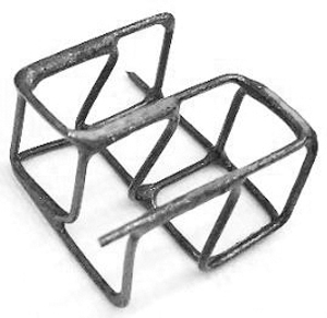
(a) Unfolded planner structure following Algorithm 2 in Appendix A2, (b) 4 × 4 × 3 cuboid cell lattice structure before node joining, and (c) wire bent structure of a hemisphere geometry (loose lattice).
TLPDB is a joining process that combines the characteristics of both brazing and diffusion bonding. In TLPDB, an interlayer (filler) metal particle containing a MPD of the substrate metals is placed between the faying surfaces. When the bonding temperature (below the substrate's melting point) is reached, the filler particles liquefy and fill the joint area by capillary action. The MPD starts diffusing into the substrate metals and forms a transient liquid phase. Due to the higher concentration of MPD at the interface, the substrate metals locally melt and the interlayer widens. Holding the joint area at the bonding temperature, MPD continues to diffuse into the substrate metals, resulting in more dilution of the interlayer, and finally undergoes isothermal solidification. The isothermal heating is continued until the bond region is homogenized.54,55 The entire bonding process is carried out in a vacuum or inert environment to prevent oxidation. TLPDB bonding can be used for a range of base metals, including Al alloys, carbon steels, stainless steels, Ni alloys, and Ti alloys. Al, Cu, Ga, In, Mg, P, Pb, B, Sb, Ag, Sn, Zn, and so on, elements are frequently used as the interlayer metals. Interlayer metals can be applied in the form of thin foil, powders, paste, electroplate, sputter, and so on.55 However, the node junctions in the loose lattice structures are hard to reach to apply the interlayer alloys in these forms. Hence, the dipping process is used to deliver the interlayer alloy to facilitate there welding using the TLPDB process.
Dip coating, a wet deposition method, is an effective and simple way of thin film/layers formation. There are four stage in the dip-coating process: (1) immersion, (2) start-up, (3) deposition, and (4) evaporation and drainage.56 Substrates are dipped in a multiphase precursor solution with homogenized dispersion of the condensed phase. Immersion speed and dwelling time are the two most important factors that determine the final film thickness, which can be a few nm up to a few μm from the same initial solution.57 Due to the inaccessible, complicated, and hierarchical architecture of our wire architecture, placing the interlayer MPD ink with traditional techniques (i.e., thin foil, paste, spraying) is a challenge.
Additionally, uniform thin (<10 μm) layer coating generated by the sputtering and electroplating process will not be sufficient to bridge the range of gaps between faying surfaces. Thus, to transfer the interlayer alloy particles into the hard to reach places, a liquid carrier (LC) system will be used. A heterogeneous mixture is constructed by adding the particles in LC, and the loose lattice will be dipped for receiving the particle at the node. As a result, the viscosity of the mixture needs to be controlled for delivering the particles in place.
Development of interlayer alloy mixture for dipping
The dipping mixture is made of commercially available TLPDB interlayer alloy Ni-based LM NicroBraz powders (procured from Wal Colmonoy Corp., Madison Heights, MI: https://www.wallcolmonoy.com). The LC system is made of a polymer and solvent. To adhere the particles at the node, as binder polymer Poly Methyl Methacrylate (Atactic PMMA; MW ∼15,000; Sigma Aldrich) is used, which is dissolved with an evaporating solvent. PMMA is a common transparent acrylic resin, known as plexiglass, that demonstrates excellent thermal stability (flash point >250°C) and tensile strength (72 MPa), satisfactory gap-filling properties, low density (∼1.17 g/cm3), and relatively harmless non-explosive and non-flammable material. The bioinert PMMA binder volatilizes at 550°C, which is almost half of the TLPDB temperature, and leaves no residue in the furnace. Therefore, the binder does not impair the bond quality. When the polymer binder volatilizes, the TLPDB alloy powders get sintered and adhere to the lattice surface. To control the viscosity suitable for dipping and sufficient material transfer, 51% (v/v) interlayer alloy is added to the binder solution to prepare the dipping mixture, as shown in Figure 8b.
Joining the lattice
Before joining the node, the loose structures are washed in acetone in an ultrasonic bath and then air-dried. The lattice structures are dipped into the mixture and retract at 10 mm/s speed. It is then kept at ambient temperature for 2 h to allow the solvent to evaporate. The organic solvent evaporates right after dipping, leaving an interlayer coat of metallic powder and polymer binder on the struts of the lattice structure. The role of the polymer binder is to hold the brazing powder particles until they start sintering during the heating cycle of the TLPDB bonding operation. The furnace was vacuumed at 10−3 torr. The temperature is raised to 580°C at a rate of 20°C/min and held there at 580°C for 20 min. The temperature was then raised to 1150°C at a rate of 20°C/min and held in there at 1150°C for 1 h and 45 min. Figure 9 shows the temperature profile of the thermal cycle used for TLPDB bonding. At high temperature, the liquid phase of interlayer alloy material diffuses into the wire material and forms a capillary bridge in the interlayer region. Bonding occurs as the interdiffusion of material changes the local composition, causing it to solidify isothermally. After furnace cooling, the maximum gap sizes are filled by melted and diffused interlayer alloy.
FIG. 9.

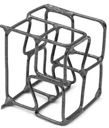
2 × 2 × 1 Unit cell fabrication with the DBDJ process: (a) green lattice, (b) glue-interlayer particle mixture, (c) dipping, (d) drying, (e) vacuum furnace heating profile, (f) raising the temperature in a vacuum furnace for TLPDB bonding, and (g) bonded lattice. TLPDB, transient liquid phase diffusion bonding.
Results and Discussion
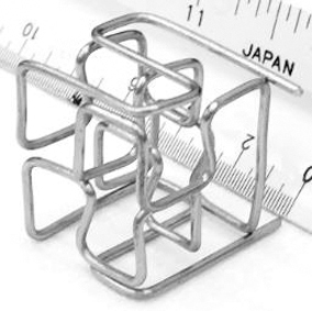
AISI1006 wire samples (diameter 1.02 mm) are designed and manufactured following the DBDJ process, as shown in Table 1 and Figure 10. Multiscale lattice structure with unit cell size from 5 mm cell to 12 mm can be seen in Figure 10, which proved the DBDJ concept. Some struts are extended by ±1.5 mm to provide better nodal contact, which caused some slanted vertical struts. Additional horizontal layers are added to the original cuboid design to ensure the structural integrity, which can be seen in the figures provided below (Table 1).
Table 1.
Cubic Lattice Structures Fabricated and Joined Following the Proposed Design, Bending, Dip, and Join Process
| Cell size and materials | Green | Coated | Joined |
|---|---|---|---|
| 10 mm, 2 × 2 × 1 Cell lattice AISI1006 |

|

|

|
| 10 mm, 2 × 2 × 2 Cell lattice AISI1006 |
|

|

|
| 12 mm, 2 × 2 × 1 Cell lattice AISI1006 |

|

|
|
| 12 mm, 2 × 2 × 2 Cell lattice AISI1006 |

|

|
|
FIG. 10.

Scalable cubic lattice structures (AISI1006 material) made from the DBDJ process.
After dipping, we observed that only one node (cell size 12 mm 2 × 2 × 2 structure) is unable to join due to the wide gap, and the liquid bride of the interlayer alloy mixture during dipping was not enough to bridge the gap. The large gap transient liquid phase (TLP) issue can be addressed by adding steel spheres (sphere 0.5–1.5 mm dia) into the liquid carrier system (LCS) (composite interlayer) to match the wide gap. The larger steel sphere will act as a space-filler to close the gap and create a bond-line similar to the medial axis compared with the traditional straight lines. Additionally, a large gap TLP joined (>2 mm) is possible and has been reported by increasing the bonding temperature at about 130°C.15
The measured relative density of the fabricated cell can range from 3.8% to 8.6%, which is shown in Table 2. The compression tests are performed using a 30 kN load cell with an Instron 5567 universal testing machine. For each type of lattice structure and cell size, two samples are tested under Z-direction loading. The crosshead speed was 3 mm/min. The results are summarized in Table 2. It has been observed that cells with higher relative density (i.e., smaller unit cell size) demonstrate higher modulus. This can be attributed to the fact that denser lattice is produced with smaller cell sizes. Additionally, for smaller cell size, the cell size to strut diameter ratio (8 mm cell to 1.02 mm) is smaller than the for larger cell size, which makes them less prone to bending or failure under compression load.
Table 2.
Compressive Strength and Relative Density of the Lattice Structure Fabricated with the Design, Bending, Dip, and Join Process
| 2 × 2 × 1 Cell |
2 × 2 × 2 Cell |
|||||
|---|---|---|---|---|---|---|
| 8 mm Cell | 10 mm Cell | 12 mm Cell | 8 mm Cell | 10 mm Cell | 12 mm Cell | |
| (MPa) | 3.15 ± 0.17 | 1.58 ± 0.26 | 1.07 ± 0.00 | 2.14 ± 0.25 | 0.93 ± 0.13 | 0.81 ± 0.05 |
| Relative density (%) | 8.6 ± 0.07 | 6.4 ± 0.17 | 5 ± 0.03 | 6.8 ± 0.11 | 5.3 ± 0.06 | 3.8 ± 0.01 |
| (MPa) | 1.72 ± 0.02 | 0.81 ± 0.47 | 0.51 ± 0.14 | 1.48 ± 0.01 | 0.45 ± 0.13 | 0.36 ± 0.01 |
TLP, transient liquid phase.
Our structures are further characterized by analyzing their performances and failure modes. Cellular structures show an exponentially decreasing mechanical performance with the reduction of density, in other words, an increase in porosity.58 Gibson and Ashby59 suggested a semi-empirical formula, also known as a power law, and densification strain to characterize the cellular structures. Their expressions are most commonly used to characterize the cellular materials, which are as follows:
| (6) |
| (7) |
Here, the above equations correlate the relationship between Young's modulus and relative density. The subscripts represent the lattice and constituent solid. The performance degradation can also be interpreted by the constituent material property, type of lattice [body centered cubic (BCC), face centered cubic (FCC), etc.],60 and the number of struts joined in each node.61 From the Maxwell number21 of a structure, it is possible to define if it is bending or stretch dominated, which has also impact on the empirical constant such as in Gibson–Ashby equations. he expected value of and for bending dominated (fixed joint) cell. Manufacturing process by which the structure is built (such as investment casting, 3D printing, and machining) can also have influence on the degradation of the mechanical performance, which has been rarely accounted previously. Similarly, captures the deformation behavior for matrix material, which has a suggested value of 3.33 and 2 for elastomeric and plastic foams. For “strain-softening” stochastic structures, the value of will be smaller than the “strain hardening” periodic structures. The value of for our fabricated structures are calculated and shown in Table 3.
Table 3.
The Performance Parameters for the Lattice Structures Fabricated with Design, Bending, Dip, and Join Process
| Sample type | Cell size (mm) | n | C1 | R2 | |
|---|---|---|---|---|---|
| 2 × 2 × 2 | 8 | 2.3338 | 0.80 | 4.41 | |
| 10 | 5.66 | ||||
| 12 | 7.89 | ||||
| 2 × 2 × 1 | 8 | 2.2516 | 0.99 | 6.39 | |
| 10 | 7.03 | ||||
| 12 | 7.4 |
We analyzed the data for the single stack (2 × 2 × 1) and double stack (2 × 2 × 2) from Table 2 and determined their value, as shown in Table 3. The lower value of C1 (<<1) is due to the low Young's modulus. The higher than suggested value of indicated a lower densification strain, which has been observed in the axial compression test. Due to the modified (slanted) vertical struts explained earlier, early densification has happened in our structures. Both materials, cell geometry and fabrication technique, can cause the lower value of.62 Compared with 3D printed 316 L and Al-Si10-Mg, our structures were built with softer annealed AISI 1006 material. To increase the nodal contact, some struts in our structure were extended by ±1.5 mm by adding an inclination angle to the column, which also makes them slanted. Although this design modification increases the nodal contact, it also facilitates the localized deformation, decreasing the compressive strength.63 In our six sample types, we have taken relative densities from 3.8% to 8.6%, which actually represents a small range of the total relative density attainable. As the data points are very close in the small range of relative densities, the value trend of the empirical constant may or may not represent the correct characteristics of the lattice structures. If we compare with the literature, our cell size to strut diameter ratios of the bending dominated cuboid (∼8, 10, and 12) are much larger than other commonly reported cell sizes. Three millimeters BCC cell with 22%64 and 4 mm Gyroid cell with 15% densities15 are reported, which are not only different from our proposed structure in cell size but also in cell topology. The minimum strut number to equilibrate the external force and moment at each node is determined analytically using the Maxwell number.65 In a cuboid structure with an axial compression load, the moment induced in each node are not equilibrated, which causes the bending dominated behavior. So, the bending dominated structures show more complaint and result in consistent deformation than stretch dominated structures such as Octet, BCC, and FCC,66 which may also be a reason for variation in results.
We have found ∼45% weight interlayer ink coat on the struts. It has been reported that the presence of excess interlayer ink deteriorates the strength of the wire.67 Post-treatment can be a good solution to strength restoration, which was not done in our case. It is possible to improve the performance by including post-processing, which provides some room for improvement. Due to bigger gaps, we observed some disjointed nodes. Although small in number, disjointed nodes can drop the mechanical performance excessively.60 From the strength-density Ashby plot,68 the compressive strengths fall into the range of metal foams for the fabricated wire lattice structure while having significant room for improvement, which makes it a promising candidate for lightweight metallic cellular structure.
Manufacturing Fidelity Analysis
We performed the manufacturing fidelity analysis for six types of lattice structures that we designed, fabricated, and joined in this work. Table 4 summarizes the relevant data for this analysis. The lattice configurations (2 × 2 × 1 and 2 × 2 × 2) are designed in Rhino 5.0 CAD software, which are then unfolded into the planner curve with the bend pattern. The length of these 2D patterns is measured in the CAD software, which is defined as the designed length for our structures. Designed mass and the designed relative density are also measured using the same CAD package shown in Table 4. The bending code is generated by using Algorithm 3 in Appendix A3, which is then fed to the laboratory developed bending machine discussed in the Bending Segment section. The feeding system in the machine pulls the designed length through two rollers for the bending tool to bend. We observed some slippage in the feeding roller during bending as the bending tool apply the bending moment causing some axial load. This slippage makes our structure larger than designed, which is measured as the actual length. Mass of the loose structure and the slippage error are also measured and shown in Table 4. The loose structures that are dipped into the prepared mixture with the volume fractions of powder, glue, and solvent were 51.33%, 4.67%, and 44%, respectively. The particles are entrapped on the loose structure with the help of polymer, which is then send to the vacuum furnace for TLPDB. We observed that the mass of joined lattice structures differed from the mass of the theoretical mass of the designed structures. This additional mass is due to the (1) weight of the extra wire from slippage and (2) weight of the interlayer ink that melts and diffused, creating a solid-state bonding. Due to this melt coat of interlayer ink, we observed an increase in wire diameter from 1.02 to 1.16 mm after TLPDB. The melt coat of interlayer ink added about ∼45% weight in the lattice structure, which contributed to the increase in the final density of those structures. However, both errors can be minimized through a systematic process parameter optimization, using more accurate control and hardware. Furthermore, by optimizing the dipping parameter and mixture composition, interlayer ink delivery can be optimized to reduce the design and manufacturing deviation and improve the manufacturing fidelity of our process.
Table 4.
Manufacturing Fidelity Analysis of the Proposed Approach
| Cell size (mm) | Lattice configuration | Design length (mm) | Designed mass (g) | Designed relative density (%) | Actual length (mm) | Bend wire mass (g) | Measured mass after TLP (g) | Measured density after TLP (%) | Powder weight before TLP (g) | Powder weight (%) | Slippage error (%) | Error in desired density (%) |
|---|---|---|---|---|---|---|---|---|---|---|---|---|
| 8 | 2 × 2 × 1 | 288 | 1.82 | 7.26 | 315 | 1.99 | 3.56 | 8.60 | 1.58 | 44 | 9.4 | 18.5 |
| 2 × 2 × 2 | 438 | 2.76 | 6.39 | 480 | 3.03 | 5.22 | 6.80 | 2.19 | 42 | 9.6 | 6.5 | |
| 10 | 2 × 2 × 1 | 360 | 2.27 | 5.03 | 389 | 2.45 | 4.46 | 6.40 | 2.01 | 45 | 8.0 | 27.2 |
| 2 × 2 × 2 | 548 | 3.46 | 4.33 | 591 | 3.73 | 7.03 | 5.30 | 3.30 | 47 | 7.9 | 22.5 | |
| 12 | 2 × 2 × 1 | 427 | 2.69 | 3.65 | 457 | 2.88 | 5.40 | 5.00 | 2.52 | 47 | 7.0 | 37.1 |
| 2 × 2 × 2 | 652 | 4.11 | 3.09 | 696 | 4.39 | 8.24 | 3.80 | 3.85 | 47 | 6.8 | 22.8 |
With our proposed process, we comfortably achieved relative density <10% and cell length to strut diameter ratio of ∼12, which may not be possible with commonly used lattice manufacturing processes. In a recent publication,69 a relative density value of 20% is reported as the lower limit for the laser-based powder bed fusion process. They also reported the strut diameter-to-cell length ratio up to 0.17. For other traditional lattice manufacturing processes (i.e., casting and joining), the rheological properties of the molten metal and the inaccessibility of the joining tools will limit the relative density values even at higher range. However, 3.5% relative density is reported as achievable by wire-woven lattice structure,67 which is comparable to the proposed DBDJ technique. Another benefit of this structure is, it is made with continuous wire, which will open up a new avenue for research and teaching on smart structures. The wire is reusable, recyclable, and the part can be easily modifiable, making it a sustainable and green manufacturing process. Some potential benefit of the process is listed in Table 5.
Table 5.
Comparison Between the Proposed Design, Bending, Dip, and Join Process and the Traditional Porous Structure Manufacturing Processes
| Cellular structure manufacturing method |
|||||
|---|---|---|---|---|---|
| Foam | Additive manufacturing/3D printing | Strucwire/wire-woven metal | Constructed lattice (sheet forming, casting and joining brazing, laser, etc.) | DBDJ (proposed) | |
| Aperiodic configuration | |||||
| Lattice pattern | Random pattern | Multiple pattern within and between layer is achievable | Single pattern | Single pattern | Multiple pattern within and between layer is achievable |
| Controllable heterogeneity/topology based progressivity/aperiodicity | Not achievable | Achievable | Not achievable | Not achievable | Achievable |
| Object shape conformity | Cut-to-fit | Shape conforming | Cut-to-fit | Cut-to-fit | Shape conforming |
| Other configuration | |||||
| Manufacturing steps | Multistage, complex process | Single- or two-stage depending on the process | Multistage, complex process, assembly required | Multistage complex process, assembly required | Two-step: bending and dipping |
| Material recycling | Very much limited | Limited to none | Limited to none | Limited to none | Direct |
| In situ design reconfiguration | Not possible | Achievable with digital thread | Not possible | Not possible | Achievable with digital thread |
| Form of material | Liquid or solid | Powder, wire or liquid | Discrete wire | Discrete wire | Continuous wire |
| Strength of structure | Low to medium | Low to medium | High | High | Low to medium |
| Number of joining nodes | n/a | Virtually infinite | Significantly high | High | Minimal |
| Multilayer structure | Limited by stacking | Achievable | Achievable | Limited by stacking single layer | Achievable |
3D, three-dimensional; DBDJ, Design, Bending, Dip, and Join.
Conclusions
The proposed DBDJ process demonstrates a novel multilayer metal lattice manufacturing technique with wire material following a systematic approach. Both periodic and aperiodic lattice structures can be manufactured with continuous thin rods by bending it with a repetitive pattern. The design segment can take the input from a traditional periodic pattern or can directly utilize the pattern information from advanced research of design science. A semi-automated process plan for the DBDJ is implemented with our laboratory-developed programmable machine. Complex shapes are often the results from topology optimization techniques, which may generate a higher order curve. The most control system can handle a large number of points and hence can be bend higher order curves. However, in this article, we restrict ourselves to the first-order geometry bend for feasibility. The fabricated cuboid metal lattice structure demonstrates promising results. Other unit types (i.e., pyramidal, hexagon, truss-like, prismatic, BCC, FCC) can also be fabricated with the proposed DBDJ process. The resulting lattices, scaffolds, or frameworks can be covered with the skin of a variety of materials to make a 3D solid appearing object. Such objects can be lightweight or very durable, depending on the desired characteristics of the object. It can often perform multiple functionalities, making it diverse and easy to manufacture, which can also be the future direction of this research. The proposed DBDJ process is highly suitable for synchronized automation and the accuracy can be improved by deploying collaborative multi-robotic assembly and by incorporating artificial intelligence in the future.
Appendices
Appendix A1. Algorithm 1: Object Voxelization
|
Input:
Output: |
Set of fitted parametric curves
Voxelized Object |
|
| 1 | //Set of voxel length along X-dir. | |
| 2 | //Set of voxel length along Y-dir. | |
| 3 | //Set of voxel length along Z-dir. | |
| 4 | //Current voxel X-Coordinate | |
| 5 | whiledo//Xmax, Xmin, Ymax, Ymin lower and upper extreme of the design space | |
| 6 | ||
| 7 | ||
| 8 | ||
| 9 | ||
| 10 | End | |
| 11 | //Current voxel Y-Coordinate | |
| 12 | while do | |
| 13 | ||
| 14 | ||
| 15 | ||
| 16 | ||
| 17 | end | |
| 18 | //Current voxel Y-Coordinate | |
| 19 | whiledo//Zmax, Zmin lower and upper extreme of the design space along Z-axis | |
| 20 | ||
| 21 | ||
| 22 | ||
| 23 | ||
| 24 | end | |
| 25 | ||
| 26 | return | |
Appendix A2. Algorithm 2: Lattice Fitting
| Input: Output: Voxelized Object , Lattice Type (e.g., Cubic, Pyramidal, Honeycomb) 3D Lattice Structure , 3D Lattice Structure Vertices |
| 1 |
| 2 |
| 3 |
| 4 for i = 1 to nz |
| 5 for j = 1 to ny |
| 6 for k = 1 to nx |
| 7 sequential vertices of according to lattice type |
| 8 next |
| 9 next |
| 10 next |
| 11 |
| 12 return , |
Appendix A3. Algorithm 3: Continuous Bending Toolpath Generation
| Input: Output: 3D Lattice Structure Vertices Continuous bending path |
| 1 |
| 2 |
| 3 |
| 4 |
| 5 for i = 1 to size(LV) |
| //toolpath vector |
| 6 |
| 7 end |
| 8 for i = 1 to size(TV) |
| 9 //wire feed length |
| 10 //bend angle |
| 11 //control axis selection |
| 12 |
| 13 end |
| 14 return |
Author Disclosure Statement
No competing financial interests exist.
Funding Information
This work was partly supported by a grant from the National Science Foundation Grant number OIA-1355466 and by a grant from Department of Transportation US-DOT number 693JK31850009CAAP.
References
- 1. Schaedler TA, Carter WB. Architected cellular materials. Annu Rev Mater Res 2016;46:187–210. [Google Scholar]
- 2. Deshpande VS, Fleck NA. Collapse of truss core sandwich beams in 3-point bending. Int J Solids Struct 2001;38:6275–6305. [Google Scholar]
- 3. Ajdari A. Mechanical behavior of cellular structures: A finite element study. Boston, MA: Northeastern University, 2008. [Google Scholar]
- 4. Wen T, Tian J, Lu TJ, et al. Forced convection in metallic honeycomb structures. Int J Heat Mass Transf 2006;49:3313–3324. [Google Scholar]
- 5. Rosen DW. Computer-aided design for additive manufacturing of cellular structures. Comput Aided Des Appl 2007;4:585–594. [Google Scholar]
- 6. Ashby MF, Evans AG, Fleck NA, et al. List of contributors. Metal foams. Burlington: Butterworth-Heinemann, 2000; pp. xi–xii. [Google Scholar]
- 7. Lee J-H, Singer JP, Thomas EL. Micro-/nanostructured mechanical metamaterials. Adv Mater 2012;24:4782–4810. [DOI] [PubMed] [Google Scholar]
- 8. Maiti A, Small W, Lewicki JP, et al. 3D printed cellular solid outperforms traditional stochastic foam in long-term mechanical response. Sci Rep 2016;6:24871. [DOI] [PMC free article] [PubMed] [Google Scholar]
- 9. Seepersad CC, Allen JK, McDowell DL, et al. Multifunctional topology design of cellular material structures. J Mech Des 2008;130:031404–031416. [Google Scholar]
- 10. Evans AG, Hutchinson JW, Fleck NA, et al. The topological design of multifunctional cellular metals. Prog Mater Sci 2001;46:309–327. [Google Scholar]
- 11. Wadley HNG, Dharmasena KP, O'Masta MR, et al. Impact response of aluminum corrugated core sandwich panels. Int J Impact Eng 2013;62:114–128. [Google Scholar]
- 12. Rashed MG, Ashraf M, Mines RAW, et al. Metallic microlattice materials: A current state of the art on manufacturing, mechanical properties and applications. Mater Des 2016;95:518–533. [Google Scholar]
- 13. Maskery I, Hussey A, Panesar A, et al. An investigation into reinforced and functionally graded lattice structures. J Cell Plast 2016;53:151–165. [Google Scholar]
- 14. Yan C, Hao L, Hussein A, et al. Ti–6Al–4V triply periodic minimal surface structures for bone implants fabricated via selective laser melting. J Mech Behav Biomed Mater 2015;51:61–73. [DOI] [PubMed] [Google Scholar]
- 15. Yang L, Mertens R, Ferrucci M, et al. Continuous graded Gyroid cellular structures fabricated by selective laser melting: Design, manufacturing and mechanical properties. Mater Des 2019;162:394–404. [Google Scholar]
- 16. Yang L, Yan C, Cao W, et al. Compression–compression fatigue behaviour of gyroid-type triply periodic minimal surface porous structures fabricated by selective laser melting. Acta Mater 2019;181:49–66. [Google Scholar]
- 17. Deshpande VS, Ashby MF, Fleck NA. Foam topology: Bending versus stretching dominated architectures. Acta Mater 2001;49:1035–1040. [Google Scholar]
- 18. Queheillalt DT, Wadley HNG. Titanium alloy lattice truss structures. Mater Des 2009;30:1966–1975. [Google Scholar]
- 19. Sennewald C, Kaina S, Weck D, et al. Metal sandwiches and metal-matrix-composites based on 3D woven wire structures for hybrid lightweight construction. Adv Eng Mater 2014;16:1234–1242. [Google Scholar]
- 20. Brackett DJ, Ashcroft IA, Wildman RD, et al. An error diffusion based method to generate functionally graded cellular structures. Comput Struct 2014;138:102–111. [Google Scholar]
- 21. Maxwell JC. On the calculation of the equilibrium and stiffness of frames. Philos Mag 1864;27:294. [Google Scholar]
- 22. Ferro C, Varetti S, Vitti F, et al. A robust multifunctional sandwich panel design with trabecular structures by the use of additive manufacturing technology for a new de-icing system. Technologies 2017;5:35. [Google Scholar]
- 23. Wadley HNG. Multifunctional periodic cellular metals. Philos Trans A Math Phys Eng Sci 2006;364:31–68. [DOI] [PubMed] [Google Scholar]
- 24. Zhao L, Ha S, Sharp KW, et al. Permeability measurements and modeling of topology-optimized metallic 3-D woven lattices. Acta Mater 2014;81:326–336. [Google Scholar]
- 25. Cheung KC, Gershenfeld N. Reversibly assembled cellular composite materials. Science 2013;341:1219–1221. [DOI] [PubMed] [Google Scholar]
- 26. Echeta I, Feng X, Dutton B, et al. Review of defects in lattice structures manufactured by powder bed fusion. Int J Adv Manuf Technol 2020;106:2649–2668. [Google Scholar]
- 27. Mun J, Yun B-G, Ju J, et al. Indirect additive manufacturing based casting of a periodic 3D cellular metal—Flow simulation of molten aluminum alloy. J Manuf Process 2015;17:28–40. [Google Scholar]
- 28. Schaedler TA, Jacobsen AJ, Torrents A, et al. Ultralight metallic microlattices. Science 2011;334:962–965. [DOI] [PubMed] [Google Scholar]
- 29. Zheng X, Lee H, Weisgraber TH, et al. Ultralight, ultrastiff mechanical metamaterials. Science 2014;344:1373–1377. [DOI] [PubMed] [Google Scholar]
- 30. Yetna N'Jock M, Camposilvan E, et al. Characterization of 100Cr6 lattice structures produced by robocasting. Mater Des 2017;121:345–354. [Google Scholar]
- 31. Jiang S, Sun F, Zhang X, et al. Interlocking orthogrid: An efficient way to construct lightweight lattice-core sandwich composite structure. Compos Struct 2017;176:55–71. [Google Scholar]
- 32. Chen X, Wu X, Shao S, et al. Hybrid printing metal-mesh transparent conductive films with lower energy photonically sintered copper/tin ink. Sci Rep 2017;7:13239. [DOI] [PMC free article] [PubMed] [Google Scholar]
- 33. Peng E, Wei X, Garbe U, et al. Robocasting of dense yttria-stabilized zirconia structures. J Mater Sci 2018;53:247–273. [Google Scholar]
- 34. Wadley HNG. Multifunctional periodic cellular metals. Philos Trans Math Phys Eng Sci 2006;364:31–68. [DOI] [PubMed] [Google Scholar]
- 35. Wang X-T, Li X-W, Ma L. Interlocking assembled 3D auxetic cellular structures. Mater Des 2016;99:467–476. [Google Scholar]
- 36. Fleck NA. An overview of the mechanical properties of foams and periodic lattice materials. Cell Metal Polym 2004:3–7. [Google Scholar]
- 37. Bauer J, Meza LR, Schaedler TA, et al. Nanolattices: An emerging class of mechanical metamaterials. Adv Mater 2017;29:1701850. [DOI] [PubMed] [Google Scholar]
- 38. Compton BG, Lewis JA. 3D-printing of lightweight cellular composites. Adv Mater 2014;26:5930–5935. [DOI] [PubMed] [Google Scholar]
- 39. Yang K, Wang J, Jia L, et al. Additive manufacturing of Ti-6Al-4V lattice structures with high structural integrity under large compressive deformation. J Mater Sci Technol 2019;35:303–308. [Google Scholar]
- 40. Lozanovski B, Leary M, Tran P, et al. Computational modelling of strut defects in SLM manufactured lattice structures. Mater Des 2019;171:107671. [Google Scholar]
- 41. Yang L, Harrysson O, Cormier D, et al. Additive manufacturing of metal cellular structures: Design and fabrication. JOM 2015;67:608–615. [Google Scholar]
- 42. Mishra DK, Pandey PM. Experimental investigation into the fabrication of green body developed by micro-extrusion-based 3D printing process. Polym Compos 2020;41:1986–2002. [Google Scholar]
- 43. Maskery I, Sturm L, Aremu AO, et al. Insights into the mechanical properties of several triply periodic minimal surface lattice structures made by polymer additive manufacturing. Polymer 2018;152:62–71. [Google Scholar]
- 44. Sagbas B. Post-processing effects on surface properties of direct metal laser sintered AlSi10Mg parts. Metals Mater Int 2020;26:143–153. [Google Scholar]
- 45. Yadav P, Rigo O, Arvieu C, et al. In situ monitoring systems of the SLM process: On the need to develop machine learning models for data processing. Crystals 2020;10:524. [Google Scholar]
- 46. Tibbits S. The emergence of “4D printing.” TED Talk. [Online]. Available at https://www.ted.com/talks/skylar_tibbits_the_emergence_of_4d_printing (last accessed June 10, 2020).
- 47. Huang T-Y, Huang H-W, Jin DD, et al. Four-dimensional micro-building blocks. Sci Adv 2020;6:eaav8219. [DOI] [PMC free article] [PubMed] [Google Scholar]
- 48. Kuang X, Roach DJ, Wu J, et al. Advances in 4D printing: Materials and applications. Adv Funct Mater 2019;29:1805290. [Google Scholar]
- 49. Leong TG, Zarafshar AM, Gracias DH. Three-dimensional fabrication at small size scales. Small 2010;6:792–806. [DOI] [PMC free article] [PubMed] [Google Scholar]
- 50. Siegel AC, Phillips ST, Dickey MD, et al. Foldable printed circuit boards on paper substrates. Adv Funct Mater 2010;20:28–35. [Google Scholar]
- 51. Ahsan AMM, Xie RN, Khoda B. Heterogeneous topology design and voxel-based bio-printing. Rapid Prototyp J 2018;24:1142–1154. [Google Scholar]
- 52. Yang L, Yan C, Fan H, et al. Investigation on the orientation dependence of elastic response in Gyroid cellular structures. J Mech Behav Biomed Mater 2019;90:73–85. [DOI] [PubMed] [Google Scholar]
- 53. Ahsan A, Khoda B.. Characterizing novel honeycomb infill pattern for additive manufacturing. J Manuf Sci Eng 2020: pp. 1–13. [Google Scholar]
- 54. MacDonald WD, Eagar TW. Transient liquid phase bonding. Annu Rev Mater Sci 1992;22:23–46. [Google Scholar]
- 55. Cook GO, Sorensen CD. Overview of transient liquid phase and partial transient liquid phase bonding. J Mater Sci 2011;46:5305–5323. [Google Scholar]
- 56. Płóciennik P, Zawadzka A, Frankowski R, Korcala A. “Selected methods of thin films deposition and their applications,” 2016 18th International Conference on Transparent Optical Networks (ICTON), Trento, Italy, 2016; pp. 1–4, doi: 10.1109/ICTON.2016.7550650. [DOI] [Google Scholar]
- 57. Grosso D. How to exploit the full potential of the dip-coating process to better control film formation. J Mater Chem 2011;21:17033–17038. [Google Scholar]
- 58. Chen W, Watts S, Jackson JA, et al. Stiff isotropic lattices beyond the Maxwell criterion. Sci Adv 2019;5:eaaw1937. [DOI] [PMC free article] [PubMed] [Google Scholar]
- 59. Gibson LJ, Ashby MF. Cellular Solids: Structure and Properties. Cambridge: Cambridge University Press, 1997. [Google Scholar]
- 60. Chen W, Liu Z, Robinson HM, et al. Flaw tolerance vs. performance: A tradeoff in metallic glass cellular structures. Acta Mater 2014;73:259–274. [Google Scholar]
- 61. Li C, Lei H, Zhang Z, et al. Architecture design of periodic truss-lattice cells for additive manufacturing. Addit Manuf 2020;34:101172. [Google Scholar]
- 62. Khoda B, Ahsan AMMN, Shovon AN, et al. 3D metal lattice structure manufacturing with continuous rods. Sci Rep 2021;11:434. [DOI] [PMC free article] [PubMed] [Google Scholar]
- 63. Huang Y, Xue Y, Wang X, et al. Mechanical behavior of three-dimensional pyramidal aluminum lattice materials. Mater Sci Eng A 2017;696:520–528. [Google Scholar]
- 64. Maskery I, Aboulkhair NT, Aremu AO, et al. A mechanical property evaluation of graded density Al-Si10-Mg lattice structures manufactured by selective laser melting. Mater Sci Eng A 2016;670:264–274. [Google Scholar]
- 65. Maconachie T, Leary M, Lozanovski B, et al. SLM lattice structures: Properties, performance, applications and challenges. Mater Des 2019;183:108137. [Google Scholar]
- 66. Ashby MF. The properties of foams and lattices. Philos Trans A Math Phys Eng Sci 2006;364:15–30. [DOI] [PubMed] [Google Scholar]
- 67. Kang K-J. Wire-woven cellular metals: The present and future. Prog Mater Sci 2015;69:213–307. [Google Scholar]
- 68. Moongkhamklang P, Deshpande VS, Wadley HNG. The compressive and shear response of titanium matrix composite lattice structures. Acta Mater 2010;58:2822–2835. [Google Scholar]
- 69. Sola A, Defanti S, Mantovani S, et al. Technological feasibility of lattice materials by laser-based powder bed fusion of A357.0. 3D Print Addit Manuf 2020;7:1–7. [DOI] [PMC free article] [PubMed] [Google Scholar]