

ABSTRACT
Emerging van der Waals (vdW) magnets provide a paradise for the exploration of magnetism in the ultimate two-dimensional (2D) limit, and the construction of integrated spintronic devices, and have become a research frontier in the field of low-dimensional materials. To date, prototypical vdW magnets based on metals of the first transition series (e.g. V, Cr, Mn and Fe) and chalcogen elements suffer from rapid oxidation restricted by the Hard-Soft-Acid-Base principle, as well as low Curie temperatures (TC), which has become a generally admitted challenge in 2D spintronics. Here, starting from air-unstable Cr2Ge2Te6 vdW thin flakes, we synthesize Ge-embedded PtTe2 (namely PtTe2Ge1/3) with superior air stability, through the displacement reaction in the Cr2Ge2Te6/Pt bilayer. In this process, the anomalous substitution of Cr with Pt in the thermal diffusion is inverse to the metal activity order, which can be attributed to the compatibility between soft-acid (Pt) and soft-base (Te) elements. Meanwhile, the layered uniform insertion of Ge unbalances Pt–Te bonds and introduces long-range ordered ferromagnetism with perpendicular magnetic anisotropy and a Curie temperature above room temperature. Our work demonstrates the anti-metal-activity-order reaction tendency unique in 2D transition-metal magnets and boosts progress towards practical 2D spintronics.
Keywords: vdW magnets, room-temperature ferromagnetism, air stability, HSAB, PtTe2Ge1/3
A novel van der Waals ferromagnet PtTe2Ge1/3 with above room-temperature Curie temperature and high air stability was synthesized through an anti-metal-activity-order displacement reaction in Pt/Cr2Ge2Te6 heterostructure.
INTRODUCTION
Since their discovery, two-dimensional (2D) van der Waals (vdW) crystals have opened up exciting prospects for next-generation integrated circuits, photoelectronics and topological electronics [1–6]. With both exchange interaction and magnetic anisotropy, magnetism is also able to survive in 2D systems [7,8], which enriches our fundamental understanding of magnetism and adds a different functional dimension to 2D materials, creating potential applications in magnetic memories and magnetoresistance sensors [9–11]. Prototypical spintronic devices based on Cr2Ge2Te6 (CGT) [12–17], CrI3 [18–21] and Fe3GeTe2 [22–25] have been realized experimentally, and exhibit fine interfaces that create unique interfacial effects in magnetic heterostructures [25,26], and distinct dimensions inherent to 2D materials, such as the stacking order [27,28], for the regulation of magnetic properties. Up to now, the low Curie temperature (TC) and the rapid degradation of magnetism in air have seriously impeded the practical applications of vdW magnets, and this has become the research focus of 2D materials.
Great efforts have been made with regard to the challenge of raising the TC of vdW magnets. 1T phase transition-metal di-chalcogenides (TMDs), such as MnSe2 [29], VSe2 [30] (in doubt [31]) and CrTe2 [32,33], were found to show the room-temperature TC, but possess rather weak stability, bringing about difficulties in synthesis and device fabrication. The ionic gating [22], change of composition [34] and proximity effect from a strong spin-orbit coupling layer (such as Bi2Te3) [35] were proven to effectively elevate the TC of vdW Fe3GeTe2 thin flakes. Although the results of raising the TC to room temperature are inspiring, the ionic gating leads to weak magnetization with negligible remanence (<10%), and the sensitive topological insulator is still a severe obstacle. Most importantly, the above methods are still unable to solve the problem of the magnetism degradation of vdW thin flakes in air and have low compatibility with the Si-based CMOS (complementary metal-oxide-semiconductor) technique. Therefore, vdW magnetic thin films with combined room-temperature TC and air-stable ferromagnetism remain unrealized and vigorously pursued.
We comprehend that the air stability of conventional vdW magnets composed of hard acids (3d transition metals, e.g. Cr3+, Fe3+ and Mn4+) and soft bases (S2–, Te2–, I–) is naturally restricted by the Hard-Soft-Acid-Base (HSAB) principle [36], in which the incompatibility between the cations and anions results in rapid oxidation even in comparably thick samples (tens of nanometers) [17,33], thus a protective layer is required in devices [25,33]. In this work, starting from CGT, we prepared layered uniformly Ge-embedded PtTe2 (i.e. PtTe2Ge1/3) by substituting Cr with Pt in the precursor framework CGT via thermal diffusion. Such an anti-metal-activity-order displacement reaction is driven by the strong affinity between Pt and Te from the HSAB principle, which reduces the total energy. The layered Ge atoms from original CGT are the natural source of uniform doping in PtTe2, in which 5d transition metal Pt is close to the Stoner criterion and has the opportunity to contribute to the ferromagnetism. Thus, long-range ordered ferromagnetism is realized. Consequently, the novel vdW magnet, PtTe2Ge1/3, shows ferromagnetism above room temperature, which is associated with robust perpendicular magnetic anisotropy (PMA) (remanence ∼80% at 300 K) and high air stability in thin flakes with the thickness down to 10 nm. The present findings will provide a unique synthesis pathway for vdW magnets and advance practical 2D spintronics.
RESULTS
Generally, vdW non-magnets consisting of soft-acid (Pt, W) and soft-base elements (Se, Te), such as PtTe2, are hardly oxidized in air, except in a 2D limit with quite a large specific surface area. Despite this, without effective doping, PtTe2 itself is non-magnetic or merely exhibits short-range magnetism from intrinsic defects at extremely low temperatures (below 40 K) [37,38]. Therefore, introducing layered ordered doping into PtTe2 with non-magnetic atoms is a promising way to induce air-stable and long-range ordered ferromagnetism above room temperature. However, inducing large amount of doping by conventional methods of film growth (such as molecular beam epitaxy and chemical vapor deposition) tends to form segregated doping or second phases, unfavorable for the emergence of stable structures and robust ferromagnetism. Enlightened by the ordered arrangement of Ge atoms in CGT, we proposed a thermal diffusion reaction in which Cr is replaced with Pt while Ge ordering is maintained, the schematic of which is shown in Fig. 1a.
Figure 1.

Schematic of the reaction and structural characterizations of PtTe2Ge1/3. (a) Schematic of the phase transition dominated by the HSAB principle during the thermal diffusion reaction. (b) HAADF-STEM cross-sectional image of the reacted t = 14 nm sample. (c) Atomic-resolution EDS mapping of Pt and Te elements. (d) Raman spectrum of the obtained sample. The inset shows the lattice structure of PtTe2. (e) EDS mapping of the Ge element. (f) EELS spectra of vdW PtTe2Ge1/3 (blue square, obtained from the integrated spectrum of EELS area mapping) and the substituted Cr on the surface (red square). The double peaks around 584 eV, and single peaks around 532 eV and 615 eV, are features of Cr, O and Te, respectively. The inset shows the low-resolution image. The crystallized Cr is highlighted by a red square. Scale bar: 2 nm. The top bright layer in the image is the protective layer (platinum) for the preparation of STEM samples.
 |
This anomalous substitution can be driven by the stronger affinity of Pt (soft acid) and Te (soft base) according to the HSAB theory, in which Te 5p electrons disperse to Pt d2sp3 hybridized orbitals, effectively preventing the oxidization of anions.
Based on this design, a 6 nm Pt film was initially deposited on the Si/SiO2 substrate, followed by the exfoliation of vdW CGT thin flakes on it (Fig. S1). Then the Pt/CGT heterostructure was heated at 400°C in a vacuum for 4 hours in order to stimulate a sufficient thermal diffusion reaction between Pt and CGT. We then used high-angle annular dark-field scanning transmission electron microscopy (HAADF-STEM) imaging to investigate the structure after the reaction. A typical HAADF-STEM cross-sectional image of the thickness t = 14 nm sample is shown in Fig. 1b. Remarkably, a uniform layered structure with vdW gaps exists in the sample, which possesses a different structure from CGT, demonstrating the formation of a different 2D material. The atomic energy dispersive spectrometer (EDS) mapping of the cross section discloses that Pt and Te atoms construct the crystal lattice (Fig. 1c), giving rise to the PtTe2 framework [39], as highlighted in the inset. The Raman spectrum shown in Fig. 1d)exhibits the double characteristic modes of PtTe2, Eg and A1g, respectively arising from the in-plane vibration and out-of-plane vibration of the Pt–Te bond. Compared with the double characteristic modes of the Cr–Te bond in CGT (Fig. S1), the Eg modes of Pt–Te in PtTe2 and Cr–Te in CGT are naturally close to each other [12,39]. Nevertheless, the complete disappearance of the A1g mode from Cr–Te and its full replacement by Pt–Te demonstrate the absence of Cr–Te bonds from CGT. This observation supports the complete phase transition from CGT to PtTe2, whose lattice structure is shown in the inset of Fig. 1d. The micro region X-ray photoelectron spectroscopy (XPS) measurement of the surface detects Pt with positive valance states and Te from PtTe2 simultaneously. The atomic ratio between Pt and Te is around 1 : 2 (Section S3). The migration of Cr to the surface after its substitution also reflects that the reaction has taken place thoroughly. From the EDS mapping of the Ge element in Fig. 1e, the Ge atoms disperse all over the vdW layers and form the layered structure in the framework of PtTe2, arising from the original layered distribution of Ge atoms in CGT. By overlapping the EDS mapping of the Ge element with the HAADF image in Fig. 1e, it is found that the EDS signal of Ge mostly appears around the Te atoms without segregation, as highlighted in the inset of Fig. 1e, indicating the uniform insertion of Ge atoms. Therefore, considering the zone axis of the HAADF image, the majority of Ge atoms are aligned with Te in the atomic column along 〈2 0〉 crystallographic orientation (in hexagonal primitive cell). Note that due to the insertion of Ge, the lattice parameter for one vdW layer is calculated to be 0.42 nm, which is slightly larger than the 0.4 nm of stoichiometric PtTe2.
In contrast, the substitution process is complete and almost no Cr atom remains in the transformed vdW material (below the measurement accuracy of EDS). Through electron energy loss spectroscopy (EELS), the substituted Cr is found to crystallize dispersedly outside the vdW layers, as shown in Fig. 1f. At local positions on the surface (red square in Fig. 1f), the Cr element exhibits strong characteristic peaks around 584 eV with the appearance of the O element at 532 eV due to the easy oxidization of Cr. In contrast, in the EELS spectrum, which is the integral of EELS area mapping (Fig. S2) obtained from the vdW layers below the surface (blue square in Fig. 1), only a strong wide characteristic peak of the Te element is observed, indicating the absence of residual Cr in the PtTe2 structure. The results of the EELS area mapping and line mapping both demonstrate the complete phase transition (Fig. S2 and Table S1), which is also demonstrated through XPS measurements with depth analysis (Fig. S4). EDS measurements are also performed to characterize the substituted Cr, which is dispersed in segregated microcrystals outside the 2D layers without the formation of a film (Fig. S5). The XPS further illustrates the oxidization and dispersion of accumulated Cr on the surface (Fig. S3). Hence the complete phase transition of CGT/Pt through the thermal diffusion reaction is in line with our expectation. In accordance with the main framework of PtTe2, which is observed through the TEM and Raman measurements in Fig. 1, we call this novel vdW magnet Ge-embedded PtTe2. The atomic ratio between Te and embedded Ge is identified through the results of EDS mapping, and the chemical formula of the vdW magnet is defined as PtTe2Ge1/3. Another significant feature of the EELS spectrum of obtained PtTe2Ge1/3 is the absence of an O peak compared to the easily oxidized Cr microcrystals in Fig. 1f, after the cross-section TEM sample exposed in air. This feature primarily reflects the high oxidation resistance of PtTe2Ge1/3, which is consistent with our proposal and will be characterized in detail below. It is worth mentioning that the synthesis process has no requirements for the substrate and both the mechanical exfoliation and wet transfer processes [40] are highly feasible when it comes to transferring the samples from the Si/SiO2 substrate, which suggests the flexibility of this vdW material.
Limited by the amount of diffused Pt atoms, the phase transition to PtTe2Ge1/3 is incomplete in much thicker samples compared to the complete transition in thin samples, as demonstrated in Fig. 1. Therefore, the incomplete transition from CGT to PtTe2Ge1/3 in the thick sample can be employed to illustrate the detailed process of the thermal diffusion reaction. Figure 2a displays a low-resolution HAADF-STEM image of the cross section of the t = 80 nm sample. Obviously, there are two areas with distinct contrast in the vdW materials. The upper dark layer keeps pristine CGT without Pt due to the insufficient diffusion, as shown in Fig. 2b. Below this layer, a transition zone exists (Fig. 2c), where Ge-embedded PtTe2 emerges below the CGT layer, indicating the phase transition from CGT to Ge-embedded PtTe2. In the lower bright layer, the crystal is also not homogeneous, exhibiting both bright and dark parts. Based on the magnified images shown in Fig. 2d)and e, the bright and dark parts are found to be Ge-embedded PtTe2 and CrTe2, respectively. Because of the differences on both the space group and stoichiometry between CGT and PtTe2, the phase transition directly from CGT to PtTe2 is inaccessible. The observed CrTe2 bridges the phase transition between them.
Figure 2.

Structural characterizations of the 80 nm sample. (a) Low-resolution HAADF-STEM image of the cross section of the reacted t = 80 nm sample. Magnified HAADF-STEM images from the upper to lower regions, (b) the CGT layer, (c) transition area, (d) PtTe2Ge1/3 and (e) CrTe2. (f) Lattice structure variation and corresponding calculated energy for Pt replacing Cr, with the formation of PtTe2. DCD of Pt atoms between two layered CrTe2 from the (g) side view and (h) top view (isosurface value of 0.007 e/Bohr3). Red and green isosurface contours indicate the charge accumulation and reduction, respectively.
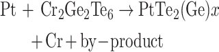
We then address the question of how the phase transition occurs and present a plausible mechanism. During the thermal diffusion reaction, Pt atoms from the bottom layer diffuse into CGT and induce the decomposition of CGT to CrTe2 and GeTe, as described by the first step in reaction equation (1).
 |
(1) |
Through calculations of the total energy, we investigate the phase transition from CrTe2 to PtTe2. Corresponding data are shown in Fig. 2f. When Pt atoms are adjacent to CrTe2, the Pt atoms tend to immigrate into the CrTe2 layer and bond with Te atoms to reduce the total energy from –18.896 eV per unit cell (u.c.) to –19.254 eV/u.c., reflecting the energy preference to form PtTe2. This is shown by the second step in reaction equation (1). This process is bolstered by the calculation of the differential charge density (DCD), whose side view and top view are illustrated in Fig. 2g)and h, respectively. When Pt atoms are inserted between two CrTe2 vdW layers, an obvious charge redistribution occurs between Pt and interlayered Te. The charge accumulates around the d orbitals of Cr, near the interlayered Te, indicating that Pt atoms are bonded with the interlayered Te atoms and weaken the adjacent Cr–Te bonds. Therefore, Pt prefers to substitute Cr to form a Pt–Te octahedron, in which the HSAB principle [36] prevails over the metal activity sequence (Cr > Pt) and drives the phase transition. The substituted Cr atoms migrate from the vdW layer and crystallize at the bottom and top surfaces of the sample, as seen in Figs2a)and S5. Partial Ge atoms are embedded into PtTe2 [the third step in reaction equation (1)], and induce ferromagnetism. The rest of the Ge atoms volatilize in the form of small molecules of GeTe. As a result of the energy reduction and mobility of Pt atoms in CGT, the displacement reaction is theoretically able to complete itself with sufficient reaction conditions, such as enough Pt and reaction time. Nevertheless, according to the HAADF images shown in Fig. 2a)(Fig. S5), the Pt and vdW layer are separated at the bottom interface by spacers composed of Cr islands and void spaces, which originate from the substituted Cr and diffused Pt atoms, respectively. These spacers block the contact between Pt and the vdW layer and lead to the insufficiency of the diffusion reaction. The vdW layer can still stand on the substrate due to the discreteness of void spaces, with support from Cr islands.
Then we check whether enhanced ferromagnetism exists in the brand-new phase, as proposed above. The magnetization hysteresis loop of obtained PtTe2Ge1/3 (∼10 nm), measured at room temperature (300 K) by the magneto-optical Kerr effect (MOKE) in Fig. 3a, undoubtedly characterizes ferromagnetism. Remarkably, the magnetization is still robust at room temperature, with considerable remanence (>45%), indicating a TC above room temperature. The clear MOKE contrast at ± 2000 Oe displayed in the insets also supports the magnetization reversal and the ferromagnetism with the tendency of PMA at room temperature. The origin of the shape of the hysteresis loop will be discussed below. Note that the substituted Cr, dispersing in microcrystals on the surface, may confuse the origin of the room-temperature ferromagnetism. Thus, the measurement of X-ray magnetic circular dichroism (XMCD) [41,42], which is a sensitive element-specific probe of magnetic orders with surface sensitivity (detection depth ∼5 nm), was carried out. The result in Fig. 3b)exhibits the negligible difference between two X-ray absorption spectra (XAS) signals around Cr L2,3-edges [32,43], demonstrating the absence of its XMCD, which excludes any ferromagnetic order contributed by Cr in the state of crystals or other Cr compounds (such as Cr-oxides). Therefore, the ferromagnetism is contributed by the vdW PtTe2Ge1/3. We also notice a shoulder peak at 575 eV (2 eV lower than the Cr L3-edge), which most likely originates from the Te M5-edge [44,45].
Figure 3.

Magnetic characterizations and theoretical calculations. (a) Out-of-plane Kerr signal measured at 300 K. The insets show the images captured by MOKE under positive and negative magnetic fields. (b) Cr L2,3-edge X-ray absorption measurements performed using the right-circular polarized (RCP) and left-circular polarized (LCP) lights in an applied magnetic field of 4.5 kOe at 200 K; the corresponding difference of two XAS signals shows the absence of the XMCD of the Cr element. The relative intensity compared to the background is exhibited. (c) DOS calculations of Ge atoms located at the interstitial position between two Te atoms and the substitution position of Te atoms. Corresponding lattice structures are shown in the insets. Yellow, blue and green balls represent Pt, Te and Ge atoms, respectively. (d) Schematic of transport measurement set-up and an optical microscope image of the device. Scale bar: 10 μm. (e) RH–H of PtTe2Ge1/3 at representative temperatures from 200 to 370 K. (f) Arrott plots of PtTe2Ge1/3 at 300 and 370 K. (g) Kerr signals of the sample measured at room temperature after exposure in air for days. The inset exhibits the optical microscope image of the sample. Scale bar: 10 μm.
The origin of ferromagnetism is then theoretically analyzed. Based on the analysis of the Ge element by EDS mapping in Fig. 1e, the Ge atoms are mostly aligned with Te in the atomic column, along 〈2 0〉 crystallographic orientation. Therefore, there are two reasonable locations for the Ge atoms in PtTe2Ge1/3, consistent with the EDS result: the interstitial position between two adjacent Te atoms from the same atomic layer, and the substitution of Te atoms, as shown in the insets of Fig. 3c. Accordingly, we construct two structure models and calculate the spin-dependent density of states (DOS), as presented in Fig. 3c. Different from the pristine PtTe2 with spin conversed DOS (Fig. S6), a sizable ferromagnetism is generated in both structures and the ferromagnetism mainly originates from the 5d-electrons of Pt atoms and 5p-electrons of Te atoms. The introduction of the Ge atoms in PtTe2 not only slightly enlarges the lattice (Fig. 1b), but also breaks the symmetry and balanced state occupation of original Pt–Te octahedral fields, which induces magnetic moments on both Pt and Te atoms. In contrast, Ge atoms have little contribution to the magnetic moments, as demonstrated by the DOS in Fig. 3c. The electronic structures with not-fully-occupied orbitals generate magnetic moments of ∼0.8 μB and ∼2.0 μB, with the embedding of Ge atoms in the condition of insertion and substitution, respectively. Because of the uniform embedding of the Ge atoms with the layered structure and high density, exchange coupling exists among the generated magnetic moments, which is able to produce long-range ferromagnetic ordering. The TC and magnetic anisotropy of the ferromagnetism are also enhanced by the strong spin-orbit coupling (SOC) [46] in PtTe2, which enables it to persist above room temperature with PMA [35,47]. The calculation of magnetocrystalline anisotropy energy (MAE) also reveals that the out-of-plane magnetic configuration is more stable with an energy that is ∼10.3 meV and ∼1.5 meV lower than the in-plane magnetic configuration per cell, in conditions of the interstitial position between Te atoms and the substitution of Te atoms, respectively (Table S3).
We further characterize the above-room-temperature ferromagnetism of PtTe2Ge1/3 in detail. Figure 3d is a schematic of the transport measurement set-up and an optical microscope image of the device. The out-of-plane magnetic-field-dependent anomalous Hall resistance (RH–H) curves of PtTe2Ge1/3 at different temperatures, from 200 K to 370 K, are shown in Fig. 3e. The most eminent feature is that a clear hysteresis loop with a large remanence at zero field persists up to 370 K (the highest temperature of our transport equipment), indicating a TC far above room temperature. The Arrott plots in Fig. 3f, extracted from the representative RH–H loops, further demonstrate a TC above 370 K. The gradual decrease of the slope in the Arrott plots indicates the attenuation of ferromagnetism from 300 K to 370 K due to thermal fluctuation. We emphasize that, distinct from conventional vdW magnets with magnetic element-based magnetism, the ferromagnetism induced in the present vdW magnets possesses high air stability. The EELS spectrum of the PtTe2Ge1/3 cross-section TEM sample (Fig. 1f), after being exposed in air, shows no signal of the O element, directly reflecting its high oxidation resistance. XPS data show the high stability (Fig. S4). Therefore, the ferromagnetic PtTe2Ge1/3 thin flakes (∼10 nm) are endowed with high air stability and show hardly any change in morphology and structure after being exposed in air for weeks, which is in stark contrast to the oxidization of conventional vdW magnetic CGT (Fig. S7). The substituted Cr in the form of segregated microcrystals, rather than a film on the surface (Figs S3 and S5), cannot prevent direct contact with oxygen from the top and side surfaces, which has no effect on air stability. Figure3g)shows the variation in magnetism of PtTe2Ge1/3 with time, measured by MOKE at room temperature without protection. Compared to the rapid oxidation in conventional vdW magnets, the sample shown in the inset exhibits stable ferromagnetism after 40 days, with negligible degradation and slight reduction of coercivity. This behavior is identical in other samples (Fig. S8). Compared to other vdW thin flake systems with air stability but a much lower TC, such as CrSe2/WSe2 with a TC below 130 K [48], the above-room-temperature and air-stable ferromagnetism in present vdW PtTe2Ge1/3 advances the practical applications of vdW magnets.
Magnetism is also found to be relevant to thickness, and Fig. 4 shows the TC as a function of the total sample thickness (t), which includes the Cr microcrystals on the surface. The enhancement of the TC above room temperature can be observed in samples with a thickness from t ∼ 9 to t ∼ 17 nm, in which the RH–H results of t = 10.5 nm and t = 14 nm samples are representatively presented in Fig. 4a)and b, respectively (results of other samples are exhibited in Fig. S9). For the t = 10.5 nm sample, a clear hysteresis loop is obtained at T = 300 K, while the loop shrinks to a simple ‘S’ shape as the temperature increases to 370 K, which is very close to TC. Interestingly, a square loop indicating robust PMA exists in the t = 14 nm sample, way above room temperature (Fig. 4b), with remanence ∼80% at 300 K and remanence >60% at 370 K. The hysteresis loops with a ‘bee waist’ shape observed in the thinner samples of ∼10 nm (Fig. 3a)and e, Fig. 4a) are attributed to the weakened magnetic anisotropy and the dipolar interaction that generally exists in magnetic multilayers and vdW magnets, such as Co/Pd multilayers [49] and Cr2Ge2Te6 [13,50]. And the magnetic anisotropy is enhanced when the thickness increases and dominates the square shape of the hysteresis loops in thicker samples (Fig. 4b). The attenuation of magnetic anisotropy and TC in thinner samples is due to the enhanced thermal fluctuation with decreased thickness, which is the characteristic of vdW magnetic thin flakes [7]. The variation of magnetic anisotropy with thickness, which is opposite to conventional magnetic films, also indicates that the origin of the room-temperature ferromagnetism is the vdW layered material PtTe2Ge1/3. When the thickness further increases to 30–40 nm, the TC abruptly drops way below room temperature. Figure 4c illustrates the RH–H curves recorded at 150, 170 and 200 K of the t = 31 nm sample, which exhibits a TC around 200 K. A similar behavior with a smaller coercivity and weaker PMA is observed in the t = 125 nm sample. Also visible in Fig. 4c)and d is the two-step switching at 150 K, which vanishes at higher temperatures. The separate switching indicates the coexistence of two phases in comparatively thicker samples; nevertheless, there is no magnetic coupling between the two phases (Fig. S10), and the proportion of the phase with weaker magnetic anisotropy increases with thickness.
Figure 4.

RH–H curves in the reacted CGT/Pt samples with different thicknesses. (a) t = 10.5 nm, (b) t = 14 nm, (c) t = 31 nm and (d) t = 125 nm.
The thickness-dependent ferromagnetism also reflects the process of thermal diffusion reactions. In samples with t ≤ 17 nm, the Pt atoms are able to diffuse to the whole vdW layer thoroughly, accompanied by the formation of a uniform PtTe2Ge1/3 with a TC above room temperature. The thicker samples (t ≥ 30 nm) differ dramatically. Only the lower part of the CGT can be diffused by the Pt atoms, and the phase transition to the Ge-embedded PtTe2 phase only exists in the region adjacent to the Pt layer, while the upper part keeps the CGT phase unchanged. The two layers result in two-step switching (Fig. 4c)and d), in which the ferromagnetism with stronger PMA (larger HC) and higher TC originates from the inhomogeneous transition part with the formation of discontinuous Ge-embedded PtTe2 phase. Due to the incomplete formation of Ge-embedded PtTe2 in the transition part diffused by Pt, its TC is only ∼200 K, lower than that of uniform PtTe2Ge1/3, which is obtained in thinner samples. In contrast, the CGT part contributes to the weaker counterpart with a lower TC. This part plays a more important role in magnetization as the CGT thickness is increased, resulting, somehow, in the decay of ferromagnetism (Fig. 4d). According to the thickness-dependent ferromagnetism, the above-room-temperature ferromagnetism can also be attributed to the vdW PtTe2Ge1/3 (see detailed discussion in Section S10).
CONCLUSION
In conclusion, given the difficulty of achieving room-temperature air-stable vdW magnets by conventional methods, we delicately obtained a novel 2D vdW magnet, Ge-embedded PtTe2 (PtTe2Ge1/3), through an anomalous displacement reaction driven by the HSAB principle. It shows robust ferromagnetism, combined with a TC above room temperature, PMA and high air stability. The layered uniformly embedded Ge atoms result in long-range ordered ferromagnetism contributed by both Pt-5d and Te-5p electrons. Meanwhile, the compatibility of soft-acid Pt and soft-base Te ensures high air stability. Other methods of preparing similar ordered-doping vdW magnets, such as molecular beam epitaxy or chemical vapor deposition, are much anticipated. Our findings represent a significant step towards practical spintronics based on 2D vdW magnets and creates the potential to explore phase transitions between different vdW families.
METHODS
Sample preparation
Platinum was deposited on the Si/SiO2 substrate by magnetron sputtering, with a vacuum higher than 10–7 Torr. CGT flakes were then exfoliated using polydimethylsiloxane. No protective layer was deposited after the exfoliation of CGT. The heating process was also performed in the magnetron sputtering system with a vacuum higher than 10–7 Torr.
Materials characterizations
Raman analysis was carried out using a HORIBA Raman microscope with an excitation wavelength of 532 nm. The thicknesses of the samples were measured by an atomic force microscope and the detailed results are shown in Fig. S11. Cross-section samples were fabricated by using a focused ion beam (FIB) system, with platinum deposited on the sample surface to prevent destruction by the ion beam. HAADF-STEM images, atomic resolved X-ray EDS and EELS spectra were performed on a FEI Titan Cubed Themis 18 60–300 (operated at 300 kV). Transport measurements were performed in a Quantum design physical property measurement system (PPMS). The Kerr signal and images of magnetic domains were captured by a MagVision Kerr Imaging System, which operates based on the MOKE in the polar configuration. The out-of-plane magnetization was probed and observed as different levels of brightness in the image. XAS of Cr L2,3-edge measurements were conducted in the total electron yield (TEY) detection mode using right-circular polarized (RCP) and left-circular polarized (LCP) lights in an applied magnetic field of 4.5 kOe at 200 K for the stronger signal, and vacuum pressure of 8 × 10⁻⁸ Torr at Beamline BL08U1A of the Shanghai Synchrotron Radiation Facility (SSRF). All spectra were obtained with the radiation normally incident to the film surface. The energy resolution of XAS was set to 0.2 eV, and the Cr L2,3-edge spectra were normalized to the maximum intensities of the Cr L3 peak. The binding energies in micro-region XPS measurements were corrected by referencing the measured C 1s peak to the value of 284.8 eV.
Device fabrication
For magneto-transport, 5-μm-wide Hall bar devices were made by photolithography and ion milling.
First-principle calculations
Our first-principle calculations were performed using the Vienna ab initio simulation package (VASP) [51,52] with projector augmented wave method [53,54]. The Perdew-Burke-Ernzerhof (PBE) functional [55] was used to treat the exchange correlation interaction and the plane-wave basis. The Gamma centered k-point mesh of 12 × 12 × 1 was used in all calculations without SOC. A vacuum layer larger than 15 Å was adopted in all calculations of thin films. DFT-D3 [56] was used to properly treat the interlayer vdW interaction. The DOS calculations of Ge-embedded PtTe2 and pristine PtTe2 were based on the same lattice constant, which was expanded to 0.46 nm for the insertion of Ge, as discussed in Fig. 3. The calculations of the total energy were also based on VASP. The MAE calculation was performed using the method GGA + SOC + U (Ueff = 3 eV for Pt [57,58]) with a Gamma centered k-point mesh of 7 × 7 × 1.
Supplementary Material
Acknowledgements
The XMCD measurement was carried out at Beamline BL08U1A at SSRF.
Contributor Information
Wenxuan Zhu, Key Laboratory of Advanced Materials, School of Materials Science and Engineering, Beijing Innovation Center for Future Chips, Tsinghua University, Beijing 100084, China.
Cheng Song, Key Laboratory of Advanced Materials, School of Materials Science and Engineering, Beijing Innovation Center for Future Chips, Tsinghua University, Beijing 100084, China.
Qian Wang, Key Laboratory of Advanced Materials, School of Materials Science and Engineering, Beijing Innovation Center for Future Chips, Tsinghua University, Beijing 100084, China.
Hua Bai, Key Laboratory of Advanced Materials, School of Materials Science and Engineering, Beijing Innovation Center for Future Chips, Tsinghua University, Beijing 100084, China.
Siqi Yin, Key Laboratory of Advanced Materials, School of Materials Science and Engineering, Beijing Innovation Center for Future Chips, Tsinghua University, Beijing 100084, China.
Feng Pan, Key Laboratory of Advanced Materials, School of Materials Science and Engineering, Beijing Innovation Center for Future Chips, Tsinghua University, Beijing 100084, China.
FUNDING
This work was supported by the National Key R&D Program of China (2021YFB3601301), the National Natural Science Foundation of China (52225106 and 51871130) and the Natural Science Foundation of Beijing Municipality (JQ20010).
AUTHOR CONTRIBUTIONS
C.S. and F.P. led the project. W.Z. and C.S. proposed the study. W.Z. prepared the samples and carried out the measurements with help from H.B. and S.Y. W.Z. and Q.W. conducted theoretical analysis. W.Z., Q.W., H.B. and C.S. wrote the manuscript. All authors discussed the results and commented on the manuscript.
Conflict of interest statement. None declared.
References
- 1. Geim AK, Grigorieva IV. Van der Waals heterostructures. Nature 2013; 499: 419–25. 10.1038/nature12385 [DOI] [PubMed] [Google Scholar]
- 2. Liu Y, Huang Y, Duan X. Van der Waals integration before and beyond two-dimensional materials. Nature 2019; 567: 323–33. 10.1038/s41586-019-1013-x [DOI] [PubMed] [Google Scholar]
- 3. Akinwande D, Huyghebaert C, Wang CHet al. Graphene and two-dimensional materials for silicon technology. Nature 2019; 573: 507–18. 10.1038/s41586-019-1573-9 [DOI] [PubMed] [Google Scholar]
- 4. Carr S, Fang S, Kaxiras E. Electronic-structure methods for twisted moiré layers. Nat Rev Mater 2020; 5: 748–63. 10.1038/s41578-020-0214-0 [DOI] [Google Scholar]
- 5. Qin X, Wang T, Jiang L. Surface engineering of nanoparticles for triggering collective properties of supercrystals. Natl Sci Rev 2017; 4: 672–7. 10.1093/nsr/nwx128 [DOI] [Google Scholar]
- 6. Otrokov MM, Rusinov IP, Blanco-Rey Met al. Unique thickness-dependent properties of the van der Waals interlayer antiferromagnet MnBi2Te4 films. Phys Rev Lett 2019; 122: 107202. 10.1103/PhysRevLett.122.107202 [DOI] [PubMed] [Google Scholar]
- 7. Gong C, Zhang X. Two-dimensional magnetic crystals and emergent heterostructure devices. Science 2019; 363: eaav4450. 10.1126/science.aav4450 [DOI] [PubMed] [Google Scholar]
- 8. Huang B, McGuire MA, May AFet al. Emergent phenomena and proximity effects in two-dimensional magnets and heterostructures. Nat Mater 2020; 19: 1276–89. 10.1038/s41563-020-0791-8 [DOI] [PubMed] [Google Scholar]
- 9. Burch KS, Mandrus D, Park JG. Magnetism in two-dimensional van der Waals materials. Nature 2018; 563: 47–52. 10.1038/s41586-018-0631-z [DOI] [PubMed] [Google Scholar]
- 10. Gibertini M, Koperski M, Morpurgo AFet al. Magnetic 2D materials and heterostructures. Nat Nanotechnol 2019; 14: 408–19. 10.1038/s41565-019-0438-6 [DOI] [PubMed] [Google Scholar]
- 11. Lin X, Yang W, Wang KLet al. Two-dimensional spintronics for low-power electronics. Nat Electron 2019; 2: 274–83. 10.1038/s41928-019-0273-7 [DOI] [Google Scholar]
- 12. Gong C, Li L, Li Zet al. Discovery of intrinsic ferromagnetism in two-dimensional van der Waals crystals. Nature 2017; 546: 265–9. 10.1038/nature22060 [DOI] [PubMed] [Google Scholar]
- 13. Wang Z, Zhang T, Ding Met al. Electric-field control of magnetism in a few-layered van der Waals ferromagnetic semiconductor. Nat Nanotechnol 2018; 13: 554–9. 10.1038/s41565-018-0186-z [DOI] [PubMed] [Google Scholar]
- 14. Hao Z, Li H, Zhang Set al. Atomic scale electronic structure of the ferromagnetic semiconductor Cr2Ge2Te6. Sci Bull 2018; 63: 825–30. 10.1016/j.scib.2018.05.034 [DOI] [PubMed] [Google Scholar]
- 15. Wang N, Tang H, Shi Met al. Transition from ferromagnetic semiconductor to ferromagnetic metal with enhanced Curie temperature in Cr2Ge2Te6 via organic ion intercalation. J Am Chem Soc 2019; 141: 17166–73. 10.1021/jacs.9b06929 [DOI] [PubMed] [Google Scholar]
- 16. Verzhbitskiy IA, Kurebayashi H, Cheng Het al. Controlling the magnetic anisotropy in Cr2Ge2Te6 by electrostatic gating. Nat Electron 2020; 3: 460–5. 10.1038/s41928-020-0427-7 [DOI] [Google Scholar]
- 17. Ostwal V, Shen T, Appenzeller J. Efficient spin-orbit torque switching of the semiconducting van der Waals ferromagnet Cr2Ge2Te6. Adv Mater 2020; 32: 1906021. 10.1002/adma.201906021 [DOI] [PubMed] [Google Scholar]
- 18. Huang B, Clark G, Navarro-Moratalla Eet al. Layer-dependent ferromagnetism in a van der Waals crystal down to the monolayer limit. Nature 2017; 546: 270–3. 10.1038/nature22391 [DOI] [PubMed] [Google Scholar]
- 19. Huang B, Clark G, Klein DRet al. Electrical control of 2D magnetism in bilayer CrI3. Nat Nanotechnol 2018; 13: 544–8. 10.1038/s41565-018-0121-3 [DOI] [PubMed] [Google Scholar]
- 20. Jiang S, Li L, Wang Zet al. Controlling magnetism in 2D CrI3 by electrostatic doping. Nat Nanotechnol 2018; 13: 549–53. 10.1038/s41565-018-0135-x [DOI] [PubMed] [Google Scholar]
- 21. Song T, Cai X, Tu MWYet al. Giant tunneling magnetoresistance in spin-filter van der Waals heterostructures. Science 2018; 360: 1214–8. 10.1126/science.aar4851 [DOI] [PubMed] [Google Scholar]
- 22. Deng Y, Yu Y, Song Yet al. Gate-tunable room-temperature ferromagnetism in two-dimensional Fe3GeTe2. Nature 2018; 563: 94–9. 10.1038/s41586-018-0626-9 [DOI] [PubMed] [Google Scholar]
- 23. Liu S, Yang K, Liu Wet al. Two-dimensional ferromagnetic superlattices. Natl Sci Rev 2020; 7: 745–54. 10.1093/nsr/nwz205 [DOI] [PMC free article] [PubMed] [Google Scholar]
- 24. Wang X, Tang J, Xia Xet al. Current-driven magnetization switching in a van der Waals ferromagnet Fe3GeTe2. Sci Adv 2019; 5: eaaw8904. 10.1126/sciadv.aaw8904 [DOI] [PMC free article] [PubMed] [Google Scholar]
- 25. Lin H, Yan F and Hu C et al. Spin-valve effect in Fe3GeTe2/MoS2/Fe3GeTe2 van der Waals heterostructures. ACS Appl Mater Interfaces 2020; 12: 43921–6. 10.1021/acsami.0c12483 [DOI] [PubMed] [Google Scholar]
- 26. Xu J, Zhu K, Hou Y. Magnetic heterostructures: interface control to optimize magnetic property and multifunctionality. ACS Appl Mater Interfaces 2020; 12: 36811–22. 10.1021/acsami.0c09934 [DOI] [PubMed] [Google Scholar]
- 27. Song T, Fei Z, Yankowitz Met al. Switching 2D magnetic states via pressure tuning of layer stacking. Nat Mater 2019; 18: 1298–302. 10.1038/s41563-019-0505-2 [DOI] [PubMed] [Google Scholar]
- 28. Li T, Jiang S, Sivadas Net al. Pressure-controlled interlayer magnetism in atomically thin CrI3. Nat Mater 2019; 18:1303–8. 10.1038/s41563-019-0506-1 [DOI] [PubMed] [Google Scholar]
- 29. O’Hara DJ, Zhu T, Trout AHet al. Room temperature intrinsic ferromagnetism in epitaxial manganese selenide films in the monolayer limit. Nano Lett 2018; 18: 3125–31. 10.1021/acs.nanolett.8b00683 [DOI] [PubMed] [Google Scholar]
- 30. Bonilla M, Kolekar S, Ma Yet al. Strong room-temperature ferromagnetism in VSe2 monolayers on van der Waals substrates. Nat Nanotechnol 2018; 13: 289–93. 10.1038/s41565-018-0063-9 [DOI] [PubMed] [Google Scholar]
- 31. Feng J, Biswas D, Rajan Aet al. Electronic structure and enhanced charge-density wave order of monolayer VSe2. Nano Lett 2018; 18: 4493–9. 10.1021/acs.nanolett.8b01649 [DOI] [PubMed] [Google Scholar]
- 32. Purbawati A, Coraux J, Vogel Jet al. In-plane magnetic domains and Neél-like domain walls in thin flakes of room temperature CrTe2 van der Waals ferromagnet. ACS Appl Mater Interfaces 2020; 12: 30702–10. 10.1021/acsami.0c07017 [DOI] [PubMed] [Google Scholar]
- 33. Sun X, Li W, Wang Xet al. Room temperature ferromagnetism in ultra-thin van der Waals crystals of 1T-CrTe2. Nano Res 2020; 13: 3358–63. 10.1007/s12274-020-3021-4 [DOI] [Google Scholar]
- 34. Liu S, Li Z, Yang Ket al. Tuning 2D magnetism in Fe3+XGeTe2 films by element doping. Natl Sci Rev 2022; 9: nwab117. 10.1093/nsr/nwab117 [DOI] [PMC free article] [PubMed] [Google Scholar]
- 35. Wang H, Liu Y, Wu Pet al. Above room-temperature ferromagnetism in wafer-scale two-dimensional van der Waals Fe3GeTe2 tailored by a topological insulator. ACS Nano 2020; 14: 10045–53. 10.1021/acsnano.0c03152 [DOI] [PubMed] [Google Scholar]
- 36. Pearson RG. Hard and soft acids and bases. J Am Chem Soc 1963; 85: 3533–9. 10.1021/ja00905a001 [DOI] [Google Scholar]
- 37. Avsar A, Ciarrocchi A, Pizzochero Met al. Defect induced, layer-modulated magnetism in ultrathin metallic PtSe2. Nat Nanotechnol 2019; 14: 674–8. 10.1038/s41565-019-0467-1 [DOI] [PMC free article] [PubMed] [Google Scholar]
- 38. Ge J, Luo T, Lin Zet al. Magnetic moments induced by atomic vacancies in transition metal dichalcogenide flakes. Adv Mater 2021; 33: 2005465. 10.1002/adma.202005465 [DOI] [PubMed] [Google Scholar]
- 39. Xu H, Wei J, Zhou Het al. High spin Hall conductivity in large-area type-II Dirac semimetal PtTe2. Adv Mater 2020; 32: 2000513. 10.1002/adma.202000513 [DOI] [PubMed] [Google Scholar]
- 40. Fan S, Vu QA, Tran MDet al. Transfer assembly for two-dimensional van der Waals heterostructures. 2D Mater 2020; 7: 022005. 10.1088/2053-1583/ab7629 [DOI] [Google Scholar]
- 41. Bansmann J, Baker SH, Binns Cet al. Magnetic and structural properties of isolated and assembled clusters. Surf Sci Rep 2005; 56: 189–275. 10.1016/j.surfrep.2004.10.001 [DOI] [Google Scholar]
- 42. Radu F, Abrudan R, Radu Iet al. Perpendicular exchange bias in ferrimagnetic spin valves. Nat Commun 2012; 3: 715. 10.1038/ncomms1728 [DOI] [PubMed] [Google Scholar]
- 43. Scariot M, Francisco MSP, Jordão MHet al. An investigation of the activation process of high temperature shift catalyst. Catal Today 2008; 133–135: 174–80. 10.1016/j.cattod.2007.12.090 [DOI] [Google Scholar]
- 44. Britz A, Attar AR, Zhang Xet al. Carrier-specific dynamics in 2H-MoTe2 observed by femtosecond soft X-ray absorption spectroscopy using an X-ray free-electron laser. Struct Dyn 2021; 8: 014501. 10.1063/4.0000048 [DOI] [PMC free article] [PubMed] [Google Scholar]
- 45. Zhang X, Lu Q, Liu Wet al. Room-temperature intrinsic ferromagnetism in epitaxial CrTe2 ultrathin films. Nat Commun 2021; 12: 2492. 10.1038/s41467-021-22777-x [DOI] [PMC free article] [PubMed] [Google Scholar]
- 46. Sasaki A, Nonaka S, Kunihashi Yet al. Direct determination of spin-orbit interaction coefficients and realization of the persistent spin helix symmetry. Nat Nanotechnol 2014; 9: 703–9. 10.1038/nnano.2014.128 [DOI] [PubMed] [Google Scholar]
- 47. Katmis F, Lauter V, Nogueira FSet al. A high-temperature ferromagnetic topological insulating phase by proximity coupling. Nature 2016; 533:513–6. 10.1038/nature17635 [DOI] [PubMed] [Google Scholar]
- 48. Li B, Wan Z, Wang Cet al. Van der Waals epitaxial growth of air-stable CrSe2 nanosheets with thickness-tunable magnetic order. Nat Mater 2021; 20: 818–25. 10.1038/s41563-021-00927-2 [DOI] [PubMed] [Google Scholar]
- 49. Chen R, Gao Y, Zhang Xet al. Realization of isolated and high-density skyrmions at room temperature in uncompensated synthetic antiferromagnets. Nano Lett 2020; 20: 3299–305. 10.1021/acs.nanolett.0c00116 [DOI] [PubMed] [Google Scholar]
- 50. Lohmann M, Su T, Niu Bet al. Probing magnetism in insulating Cr2Ge2Te6 by induced anomalous Hall effect in Pt. Nano Lett 2019; 19: 2397–403. 10.1021/acs.nanolett.8b05121 [DOI] [PubMed] [Google Scholar]
- 51. Kresse G, Furthmüller J. Efficiency of ab-initio total energy calculations for metals and semiconductors using a plane-wave basis set. Comput Mater Sci 1996; 6: 15–50. 10.1016/0927-0256(96)00008-0 [DOI] [PubMed] [Google Scholar]
- 52. Kresse G, Furthmüller J. Efficient iterative schemes for ab initio total-energy calculations using a plane-wave basis set. Phys Rev B 1996; 54: 11169–86. 10.1103/PhysRevB.54.11169 [DOI] [PubMed] [Google Scholar]
- 53. Blöchl PE. Projector augmented-wave method. Phys Rev B 1994; 50: 17953–79. 10.1103/PhysRevB.50.17953 [DOI] [PubMed] [Google Scholar]
- 54. Joubert D. From ultrasoft pseudopotentials to the projector augmented-wave method. Phys Rev B 1999; 59: 1758–75. 10.1103/PhysRevB.59.1758 [DOI] [Google Scholar]
- 55. Perdew JP, Burke K, Ernzerhof M. Generalized gradient approximation made simple. Phys Rev Lett 1996; 77: 3865–8. 10.1103/PhysRevLett.77.3865 [DOI] [PubMed] [Google Scholar]
- 56. Grimme S, Antony J, Ehrlich Set al. A consistent and accurate ab initio parametrization of density functional dispersion correction (DFT-D) for the 94 elements H-Pu. J Chem Phys 2010; 132: 154104. 10.1063/1.3382344 [DOI] [PubMed] [Google Scholar]
- 57. Setyawan W, Gaume RM, Lam Set al. High-throughput combinatorial database of electronic band structures for inorganic scintillator materials. ACS Comb Sci 2011; 13: 382–90. 10.1021/co200012w [DOI] [PubMed] [Google Scholar]
- 58. Xie Z, Lin S, Wang Z. Electronic structure and magnetism in transition metal doped InSe monolayer: a GGA + U study. Ceram Int 2018; 44: 15912–7. 10.1016/j.ceramint.2018.06.008 [DOI] [Google Scholar]
Associated Data
This section collects any data citations, data availability statements, or supplementary materials included in this article.