Abstract
In this research, a theoretical investigation of the one-dimensional defective photonic crystals is considered for the detection of gamma-ray radiation. Each unit cell of the considered one-dimensional photonic crystals (1D PhCs) is composed of two layers designed from porous silicon infiltrated by poly-vinyl alcohol polymer doped with crystal violet (CV) and carbol fuchsine (CF) dyes (doped-polymer) with different porosity. In addition, a single layer of doped-polymer is included in the middle of the designed 1D PhCs to stimulate the localization of a distinct resonant wavelength through the photonic band gap. In particular, the appearance of this resonant mode represents the backbone of our study towards the detection of γ-ray radiation with doses from 0 to 70 Gy. The Bruggeman's effective medium equation, the fitted experimental data to the refractive index of the doped-polymer, and the Transfers Matrix Method (TMM) serve as the mainstay of our theoretical treatment. The numerical findings provide significant contributions to some of the governing parameters such as the thicknesses of the considered materials on the performance of the presented sensor, the effect of incidence angle and the porosity of the considered materials on the resonance wavelength. In this regard, at optimum values of these parameters the sensitivity, quality factor, signal-to-noise ratio, detection limit, sensor resolution, and figure of merit that are obtained are 205.7906 nm RIU−1, 9380.483, 49.315, 2.05 × 10⁻⁵ RIU, 3.27 × 10⁻⁵, and 2429.31 RIU−1, respectively. Therefore, we believe that the suggested design could be of significant interest in many industrial, medical, and scientific applications.
In this research, a theoretical investigation of the one-dimensional defective photonic crystals is considered for the detection of gamma-ray radiation.
Introduction
Ionizing radiation is a type of high-energy radiation that causes ionization in the materials it passes through. It comprises non-particulate radiation, like X-rays and γ-rays, as well as radiation produced by energetically charged particles, like alpha and beta particles, or by neutrons. Ionizing radiation can alter the exposed material in a variety of ways, including biological, chemical, and physical responses.1,2 Ionizing radiation has recently become more widely used for a variety of applications.3,4 Industrial radiation processing and control, cancer cell treatment, medical sterilization, food preservation, and environmental gamma dosimetry are demonstrated among the applications where radiation dosimeters are used.3,5–7
Meanwhile, radiation dosimetry is crucial to these ionizing radiations and has attracted a lot of attention.8 There are different types of radiation dosimetry used to detect ionizing radiations.4 A scintillation dosimeter is one of the oldest types of dosimeters, which uses the scintillation light produced in particular materials. Scintillation dosimeters work on the principle that the substance being utilized can convert ionizing radiation into detectable light. It is then converted into an electrical signal using a photodiode or photomultiplier tube.9 The second type of dosimetry is known as thermoluminescence. Thermoluminescence (TL) is defined as the emission of light from a solid as a result of heat following radiation exposure. A dosimeter based on optically stimulated luminescence works similarly to a TL dosimeter. These types of dosimeters can measure very small dosages and are suited for personal and medical uses.10–12 Also, some dosimeters rely on changes in the optical fiber and use spectrophotometry to measure the change in Radiation-Induced Attenuation (RIA).8,13 Moreover, quartz fiber electroscope (QFE) dosimeters, electronic and electrical dosimeters, and film/badge personal dosimeters represent one of the most popular types. However, most of the aforementioned types have some disadvantages that appear in the form of limited shelf life, expensive price, temperature and light impacts that cause fading, and sensitivity to hard handling.13 These issues primarily raise operating costs for industrial applications. For usage in strain and temperature applications, a lot of research has been done on creating radiation-resistant Fibre Bragg Gratings (FBGs).14,15 In this regard, optical FBG sensors have proven to be advantageous in many industrial sensing applications. Their primary advantages over electronic, chemical, mechanical, and electrical sensors typically include their higher sensitivity, small size, resistance to harsh environments, immunity to electromagnetic interference, ability to be mass produced at low cost, and ability to measure remotely in real time.16 In addition, there are dosimeters based on photonic crystal fiber and Bragg gratings structures.8
Photonic Crystals (PhCs) are artificial inhomogeneous structures that can be designed or fabricated in one-dimension (1D), two-dimension (2D), or three-dimension (3D) to control and manipulate light's propagation within a specific range of frequencies called the photonic band gap(PBG).17–19 The difference in refractive indices between the constituent materials leads to the generation of this PBG. The creation of local resonance modes by creating a cavity or (defect) within the periodic structure of PhCs is utilized in sensor applications.20–22 The PhCs are a promising candidate for application in radiation dosimetry.8 This is a result of their remarkable stable behavior and post-irradiation recovery characteristics.8
When constructing the best PhCs as radiation dosimeters, there are numerous factors and characteristics to consider. The material sensitivity to radiation is the major important factor. The material's susceptibility to radiation interaction is crucial.8,23 In this study, we need a material with highly sensitive γ-rays radiation used as gamma dosimetry within the dose limits necessary for the specific applications. In this context, polymers with better surface and bulk properties have been more important during the past few decades, because of their low weight, low cost, easy processability, and ease of fabrication of thick and thin samples.24 The structural changes caused by high-energy radiation interactions with polymeric materials, such as X-rays, γ-rays, neutrons, and electrons, may allow for some fine-tuning of the materials' optical, thermal, mechanical, dielectric, and conductivity properties. Many researchers have been examining the impact of irradiation on doped polymer composite materials to probe the special features.25
Due to its high transparency and excellent flexibility, polyvinyl alcohol (PVA), which has the general formula[–CH2CH(OH)–]n, is a well-known polymer for numerous technical applications.26 The composites used in the majority of PVA works are sufficiently sensitive to either low or high-energy radiations, which impart improved or degraded physicochemical properties.25 For example, M. A. Ali Omer et al. have suggested the viability of using PVA/Cu2O composite films as radiation detectors and personal dosimeters based on optical changes sensitive to γ-rays emitted from 60Co-source in the range of (0–12) Gy suitable in rural sectors and low-income nations.11 I. M. Osman et al. show the effects of additive and gamma irradiation on the structural and optical properties of polyvinyl alcohol doped with silver nitrate.27
In this regard, porous PhCs have exceptional advantages over other ordinary PhCs.28 Materials with voids or holes are said to be porous materials. Because they have large surface areas, variable pore sizes, and a narrow pore size distribution, porous materials are essential for study.29 They can be applied in many different fields, including sensing, adsorption, and catalysis, because of these inherent features.30 The amount of void or pore spaces in a material is measured by its porosity, which is defined as the ratio of void volume to total volume.31 Porous silicon (PSi) is a variety of silicon wafers that has nanopores added to their microstructure.21,32 In 1994, Vincent used electrochemical etching to create the first PhC fabricated from PSi.33 By electrochemically anodizing crystalline silicon in a solution of hydrofluoric HF acid, porous silicon is commonly produced. The porosity determined by the anodization current density. Lower refractive index values correspond to increased porosity. It is widely believed that the electrochemical etching process in the silicon/fluoride combination is self-limiting and only happens at the interface between porous Si and crystalline substrate, meaning that the already-etched porous layer is unaffected by subsequent electrochemical etching. Consequently, the depth of the porosity can be modified. Because of this, PS multilayers with various refractive index profiles can be produced. One-dimensional photonic structures can be easily and inexpensively fabricated in this way. It has been demonstrated that a shift in the photonic feature can provide a very sensitive method for the detection of any change in the material (the optical properties of the doped polymer) that can enter the pores. The spectral peak position of a multilayer is strongly influenced by the average refractive indices of the layers.34 Additionally, numerous benefits of the PSi-1DPhCs can appear in the form of their large specific surface area, ease of manufacture, and compatibility with conventional microelectronics processing.34,35
Reliance on all of the aforementioned, we present here a new theoretical investigation of the γ-ray radiation dosimeter based on a 1D-PSi-PhC structure with a central defect layer. We are choosing 1D-PhCs due to the low cost and variety of applications.36,37 The suggested design contains two PSi-layers with different porosity, and thicknesses, besides PVA-polymer containing (CV + CF) as a defect layer. In addition, the pores of these two PSi-layers were infiltrated by PVA-polymer-containing (CV + CF). After this, we investigate the transmittance spectrum of our sensor depending on the theoretical methods that will be explained in the next part. Then we go to the result and discussion part, in which we explain how gamma rays affect the structure and materials emitted from a 60Co-radioactive source in the range of (0–70 Gy). Also, we show how the PSi-layer changed the refractive index of the doped PVA-polymer, and how the porosity of the PSi-layer affects the refractive index of the doped PVA-polymer. Then, we considered the effect of the γ-ray doses on the resonance wavelength present in PBG, and the performance of our sensor. Also, we study the effect of the geometrical parameters of our sensor such as the effect of the thicknesses of the materials composing this sensor on the resonance wavelength and the sensitivity of our sensor. According to this study, we choose the optimum value for each parameter which gives high values for performance parameters. Additionally, one of the most significant factors impacting the transmittance spectrum of a 1D-PSi-PhCs is the angle of incidence. It is therefore expected to have a significant impact on the defect mode and consequently the 1D PSi PhCs-based sensor. Also, we show how the porosity of the first and the second PSi-layers effect on the position and the intensity of the resonance wavelength. Finally, the novelty of this paper concludes in the use of the defective 1DPhC based on porous silicon infiltrated by a doped-polymer for the detection of gamma-ray radiation with the highest sensitivity without changing the experimental data of the optical properties of the doped polymer.
Basic equations and model design
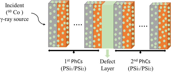
Fig. 1, shows a schematic diagram of a one-dimensional binary PhCs with a defect layer in the form [Air/(AB)N1 D (AB)N2/substrate], where A, B, and D are the PSi1, PSi2, and the defect layer, respectively. The popular experimental methods for creating PhCs or defective 1DPhCs are layer-by-layer deposition,38 anodic oxidation procedure,39,40 colloid self-assembly technology,41 and glancing angle deposition.42 Among them, the anodic oxidation procedure would be worth investigating as a highly efficient and low-cost method to prepare the DPCs integral formation because it is relatively simple to create a defective layer by adjusting the periodic voltage waveform.39,40
Fig. 1. Schematic diagram of the 1D-defective PhC. The structure of 1D-DPhC is surrounded by air and glass substrate.
In fact, many theoretical methods, including the transfer matrix method, finite-element method, and plane-wave expansion method, have been proposed for determining the optical properties of PhCs in 1D, 2D, and 3D. But when compared to its counterparts, the transfer matrix (TMM) method is thought to be the most appropriate for analyzing the cases of 1DPhCs. Based on the Maxwell equations and the boundary conditions, this method was frequently used to determine the transmittance spectrum of the electromagnetic waves that were propagating in 1DPhCs.43–45 The transmittance spectrum is investigated for the 1D-PhCs in the presence of a doped polymer as a defect layer as the following equation.
 |
1 |
where, t is the transmittance coefficient, then the parameters (Po) and (Ps) are utilized to define the optical characteristics of the starting medium (air) and substrate for a transverse electric polarization, respectively such that: -
| Po = no cos θo, and Ps = ns cos θs | 2 |
where, no, ns are the refractive index of air and substrate. m11, m12, m21, and m22 are the elements of the final matrix of the proposed structure and could be written as the following equation.
 |
3 |
where, MPSi1, MPSi2, MDoped_Polymer is the characteristic matrix for PSi1, PSi2, and doped polymer (defect layer) donated by Mj. These matrices are essentially described by the incident angle, the wavelength of the incident electromagnetic waves, the thickness of the specified layer, and its refractive index. The interaction of electromagnetic waves through individual layers (j) can be described as the following equation:36,41–43 -
 |
4 |
where, c, λ, θj, dj, and nj describe the velocity of light in a vacuum, the wavelength of the incident photons, the angle of incidence through each layer j, the thickness of layer j, and its refractive index, respectively.
Then, to determine the refractive index of the porous silicon layer, the approximation of Bruggeman's effective medium can be used as the following:21,46
 |
5 |
| ϵ = 3P(n(Polymer)2 − n(Si)2) + (2n(Si)2 − n(Polymer)2) | 6 |
where, nSi, nPolymer, and P are the refractive index of the silicon, the refractive index of the doped polymer inside the pore of the whole PSi layer, and the porosity ratio, respectively. The refractive index of the doped polymer used as a defect layer and infiltrated into the whole PSi layer is calculated by the fitting experimental data. According to the ref. 1, utilizing a solvent casting technique, film samples of the polymer, poly vinyl alcohol, carbol fuchsin, and crystal violet were prepared. These films were exposed to varying doses of 60Co-source radiation (10, 20, 30, 40, 50, 60, and 70 Gy) at room temperature.
The following fitted equation can be used to express the refractive index of the doped polymer by applying cubic fitting to the experimental data of the refractive index of the doped polymer at various γ-ray doses.1
| nD(Polymer) = αλ3 + βλ2 + γλ + δ | 7 |
where Table 1 lists the values for the constants α, β, γ, and δ. With gamma-ray radiation doses ranging from 0 Gy (unirradiated sample) to 70 Gy, the fitting's R-square value is equal to 0.015963.
Constants for the doped polymer's refractive index are provided as a function of wavelength at various gamma-ray doses (Gy).
| D γ (Gy) | α (nm−3) | β (nm−2) | γ (nm) | δ |
|---|---|---|---|---|
| 0 | 1.7479 × 10⁻⁷ | −0.00025167 | 0.11796 | −15.571 |
| 10 | 1.5689 × 10⁻⁷ | −0.00022845 | 0.1083 | −14.282 |
| 20 | 1.3002 × 10⁻⁷ | −0.00019042 | 0.090693 | −11.606 |
| 30 | 1.2167 × 10⁻⁷ | −0.00017806 | 0.084739 | −10.663 |
| 40 | 1.0444 × 10⁻⁷ | −0.00015298 | 0.07293 | −8.87 |
| 50 | 1.013 × 10⁻⁷ | −0.00014864 | 0.070913 | −8.5343 |
| 60 | 9.754 × 10⁻⁸ | −0.00014305 | 0.068283 | −8.1388 |
| 70 | 9.6042 × 10⁻⁸ | −0.00014056 | 0.067049 | −7.9382 |
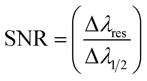
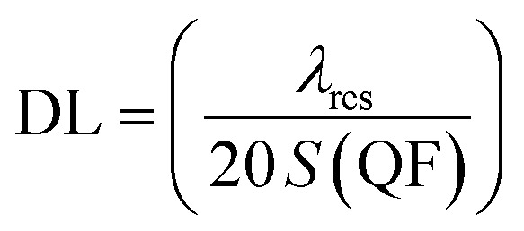
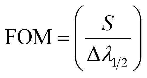
Then, the values of several factors, such as the sensitivity (S), the figure of merits (FOM), the quality factor (Q), signal-to-noise ratio (SNR), detection limit (DL), and sensor resolution (SR) could be utilized to describe the effectiveness and performance of any sensor type. The following equations can be used to acquire these parameters.29,47
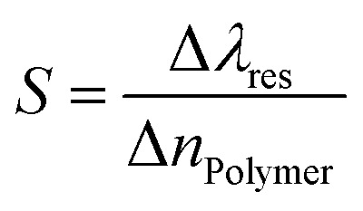 |
8 |
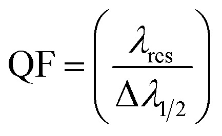 |
9 |
 |
10 |
 |
11 |
| SR = (DL)(S) | 12 |
 |
13 |
where the resonance wavelength λres, and the refractive index of the doped polymer (nPolymer) for the unirradiated sample (0 Gy) were used as references to calculate Δλres, and ΔnPolymer of irradiation samples after exposure to γ-ray doses. For example, Δλres(10 Gy) = λres(10 Gy) − λres(0 Gy), and ΔnPolymer(10 Gy) = nPolymer(10 Gy) − nPolymer(0 Gy). λ1/2 is the full width at half the maximum of the resonance wavelength.
Results and discussion
Based on the TMM and using MATLAB R2019a software, the transmittance spectrum of the proposed 1D-DPhCs based on PSi-layer is simulated. The spectral range in the visible wavelength for a transverse electric polarization (s-polarization or TE mode) is adopted. The incident radiation at an angle of incidence (θ0) is perpendicular to the plane of incidence. The refractive indices of the Si, air, and glass, are nSi = 3.7, nAir = 1, and ns = 1.52, respectively.43 The refractive index of the PSi and the defect layer (polymer) are considered based on eqn (5)–(7). The thickness of the first layer (PSi1), the second layer (PSi2), and the defect layer are, respectively, d1 = 30 nm, d2 = 73 nm, and d3 = 285 nm. The porosity of the first layer (PSi1), and the second layer (PSi2) are P1 = 30%, and P2 = 80%, respectively. For optimization, the period of numbers of the 1st PhC, and 2nd PhC are chosen to be N1 = 17, and N2 = 17, respectively. Fig. 1, shows that the polymer will be infiltrated the pores of the PSi layers and the defect layer. The sensing mechanism of our structure may be used as a gamma-ray dosimeter. One of the main objectives of this study is to create a radiation-resistant structure for use in nuclear environments for temperature and tension-sensing applications. On the experimental side, gamma-ray radiation affects the materials and the dimensions of our structure.48,49 The principal materials in our dosimeter are the doped polymer and the porous silicon layer. It is important to note that at an irradiation dose of 1000 kGy, the change in the Si refractive index is less than (5 × 10⁻⁵).48 Additionally, at 32 °C and 66.5 kGy, the thermo-optic coefficient of Si is equivalent to (2.3 × 10⁻⁴ K−1).48,50 The radiation thermal effect can raise the temperature of Si by a maximum of 3.2 °C.51 As a result, the change in Si's refractive index produced by the radiation process for doses between 0 and 70 Gy can be disregarded. Accordingly, any change in the optical properties of our dosimeter is due to the change in the optical properties of the doped polymer only as a result of the influence of doses of gamma rays between 0 and 70 Gy. The effect of gamma-ray radiation on the geometrical dimensions of our dosimeter is also disregarded. This is because Si has a low thermal expansion coefficient (≈2.6 × 10⁻⁶ K−1). In particular, the exposure of the designed structure with a dose of 66.5 kGy could raise its temperature 3.2 °C over the room temperature.49 However, this increase is not effective on the thicknesses of the constituent materials due to their very small thermal expansion coefficients. As a result, the expanding in the thicknesses of these materials is not exceeding 10−5 nm. This result can be simply investigated from the equation (Δd = d0αΔT). Thus, it is also possible to ignore the thermal strain produced by radiation. In conclusion, we believe that the suggested structure can measure gamma-ray radiation without being damaged.
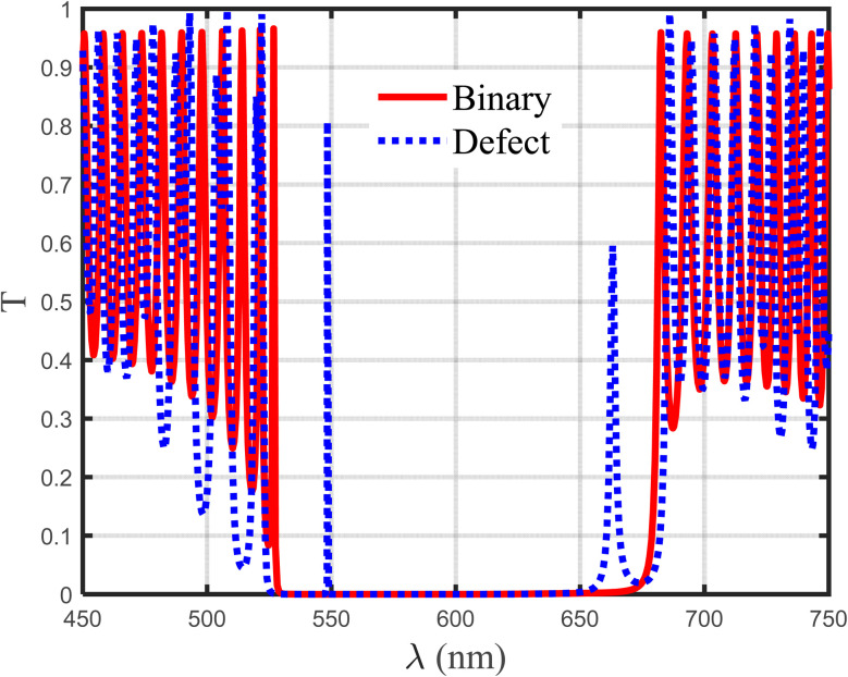
Fig. 2, illustrates the transmittance spectrum of the proposed 1D-PhC without a defect layer and with a defect layer (1D-DPhC). The values of the different geometrical parameters for the two structures are listed in Table 2. In order to achieve the best sensor performance, these parameters are calculated after optimization. We see that in the case of 1D-PhC without a defect layer, the PBG formed in the visible region with a width equal (Δλ = 678.729 − 527.486 = 151.240 nm). In addition, the intensity of the left band edge, and the right band edge equal 96%, and 95%, respectively. By inserting the doped polymer as a defect layer into the structure, the defect mode (resonance wavelength) is found at wavelength 548.365 nm with an intensity of 80%. In addition, the characteristics of the PBG are enhanced, where the width of the PBG becomes 159.53 nm, the intensity of the left band edge, and the right band edge reached 100%, and these band edges of the PBG become sharp. This defect mode is the mainstay of our designed sensor. In another word, the shift in the position of this resonant peak due to the radiation exposure describes the strategy towards the utilization of such design in the sensing and detection of Gamma radiation.
Fig. 2. Transmittance spectrum of 1D-binary and defective structure with doped PVA-polymer as a defect layer, at zero gamma-ray radiation.
The values of the geometrical parameters of the proposed structures.
| Geometrical parameters | |
|---|---|
| Values of 1D-PhC | Values of 1D-DPhC |
| d 1 = 30 (nm) d2 = 73 (nm) P1 = 30% P2 = 80% N = 35 | d 1 = 30 (nm) d2 = 73 (nm) d3 = 285 (nm) P1 = 30% P2 = 80% N1 = N2 = 17 |
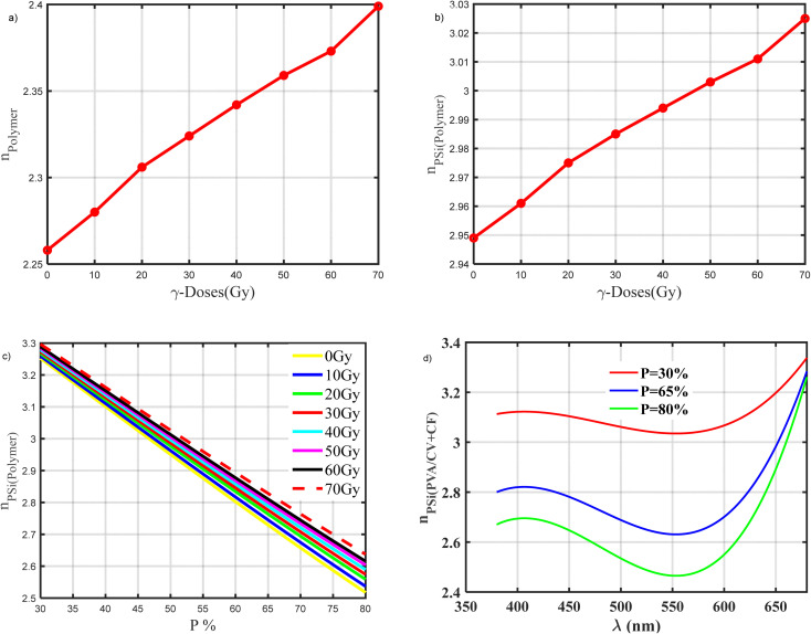
The mechanism of the proposed 1D-DPhC is based on the effect of γ-ray radiation on the refractive index of the doped polymer. This refractive index variation leads to a defect mode (resonance wavelength) shift in the transmittance spectrum. Before studying the effect of the doses of γ-ray radiation on our sensor, we need to show the effect of these doses on the refractive index of the material which constituted our sensor. In addition, we show the reason for choosing porous silicon material in our structure. Fig. 3a, shows the refractive index of the doped polymer versus the doses of γ-ray radiation from (0 to 70 Gy) at the wavelength (λ = 548.365 nm). The refractive index of the doped polymer (n(PVA/CV+CF)) increases gradually as the γ-ray doses increase. Where, n(PVA/CV+CF) increases from 2.258 to 2.399, when γ-ray doses increase from (0 to 70 Gy). According to Born and Wolf's theory, the non-enhancement of the polymer's anisotropic properties results from the development of covalent connections between different chains, which explains the increase in the polymer's refractive index after irradiation.52 In addition, the increase in the polymer's refractive index following irradiation may be the result of ionization and/or atomic displacements caused by a gamma-ray collision with the samples, which may change the internal structure of the polymer films.1Fig. 3b, shows the refractive index of the porous silicon infiltrated by doped polymer versus the doses of γ-ray radiation from 0 to 70 Gy at the wavelength (λ = 548.365 nm). It the evident that, the PSi-layer enhanced the polymer's refractive index. Where, the refractive index increases from 2.258 to 2.949 at γ-ray doses equal to 0 Gy, and from 2.399 to 3.025 at γ-ray doses equal to 70 Gy in the case of PSi-layer. Wherein, the refractive index of porous silicon is dependent on the refractive index of silicon, the refractive index of the material inside the pores (doped polymer), and the porosity value, according to Bruggeman's effective-medium approximation as eqn (5) and (6). The relationship between the PSi's refractive index and porosity variation is represented in Fig. 3c. For all wavelength values in the visible range, the refractive index of the PSi will decrease as the porosity value increases as investigated in Fig. 3d. In particular, PSi with low porosity could receive increased values of the refractive index compared to those at high porosity. Also, the PSi's refractive index decreases linearly with increasing the values of porosity after exposure to γ-ray doses from (0 to 70 Gy), as shown in Fig. 3d. We note that at the same value of porosity, the PSi's refractive index increases with an increase in the γ-ray doses. For example: at P = 30%, the PSi's refractive index is equal to 3.251, 3.266, 3.277, and 3.288 at γ-ray doses equal to 0, 20, 40, and 60 Gy, and at P = 80%, the PSi's refractive index equal 2.517, 2.558, 2.589, and 2.616 at γ-ray doses equal 0, 20, 40, and 60 Gy. After we saw the effect of the porosity ratio on the refractive index of the porous silicon layer, we chose the optimization value for each layer of porous silicon layers that achieve the highest performance of our sensor.
Fig. 3. (a) Variation in the doped polymer's refractive index as a function of γ-ray doses from (0 to 70 Gy), confined with ref. 1. (b) Variation in the PSi layer's refractive index as a function of γ-ray doses from (0 to 70 Gy), and (c) porosity ratio. At wavelength (λ = 548.365 nm). (d) The effect of porosity on the PSi layer's refractive index at (0 Gy).
Briefly, the principle of the sensing mechanism depends on the variation of the refractive index of the doped polymer which is used as a defect layer induced by exposure to γ-ray doses from (0 to 70 Gy). This reflects on the position of the defect mode which presents in PBG.
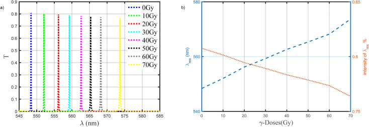
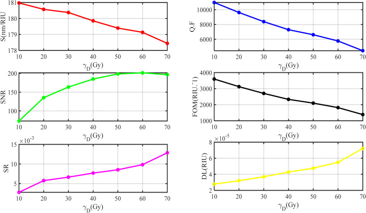
Fig. 4a, shows the effect of γ-ray doses from (0 to 70 Gy) on the resonance wavelength with the same geometrical parameters which presents in Table 2. We note that with increases in the value of γ-ray doses, the resonance wavelength shifts to a higher wavelength, and the intensity of the resonance wavelength slightly decreases. This appears in Fig. 4b, when γ-ray doses equal 0, 20, 40, and 60 Gy, the position of the resonance wavelength equals 548.365, 556.184, 562.627, and 568.213 nm, and the intensity of the resonance wavelength equals 80.756%, 79.448%, 78.338%, and 77.355%, respectively. This response is essentially dependent on the role of such parameters on the optical path length of the incident photons through the designed structure. In another meaning, the increase in the radiation dose leads to significant increments in the indices of refraction of both doped polymer and PSi as well as investigated in Fig. 3a and b, respectively. Thus, the shift in the position of the resonant wavelength and the PBG as well is expected to keep the condition of constant phase shift.17,18,20,38 Several parameters, including the sensitivity (S), the figure of merit (FoM), signal-to-noise ratio (SNR), single resolution (SR), detection limit (LD), and quality factor (Q.F), can be used to determine the effectiveness and the performance of this gamma-ray radiation sensor. These parameters' mathematical relationships can be calculated as mentioned in eqn (8)–(13). As we notice in Fig. 5, the behavior for each performance parameter appears in the accuracy of our sensor along with applied doses of γ-ray radiation. The values of these parameters are present in Table 3 at different doses of γ-ray radiation. Find the maximum value for the sensitivity of this sensor equal to 180.970 (nm RIU−1).
Fig. 4. (a) The effect of gamma-ray radiation on the transmittance spectrum of our sensor. (b) The resonance wavelength and the sensitivity at different γ-doses (Gy) from (0–70 Gy).
Fig. 5. The initial performance of our gamma-ray radiation sensor.
The initial optimum performance parameters are summarized in this table.
| D (Gy) | λ res (nm) | Intensity of λres % | Δλres (nm) | Δλ1/2 (nm) | S(nm RIU−1) | Q.F | SNR | DL (RIU) | SR | FOM (RIU−1) | n (d) | Δ n(d) |
|---|---|---|---|---|---|---|---|---|---|---|---|---|
| 0 | 548.3655 | 0.80756 | — | 0.0452 | — | 12 131 | — | — | — | — | 2.2580 | — |
| 10 | 552.0392 | 0.80147 | 3.6737 | 0.0503 | 180.9704 | 10 974.93 | 73.035 | 2.78 × 10⁻⁵ | 2.78 × 10⁻³ | 3597.82 | 2.2783 | 0.0203 |
| 20 | 556.1842 | 0.79448 | 7.8187 | 0.0578 | 180.5704 | 9622.56 | 135.27 | 3.20 × 10⁻⁵ | 5.77 × 10⁻³ | 3124.05 | 2.3013 | 0.0433 |
| 30 | 559.2781 | 0.78918 | 10.9126 | 0.0667 | 180.3735 | 8384.97 | 163.60 | 3.69 × 10⁻⁵ | 6.65 × 10⁻³ | 2704.25 | 2.3185 | 0.0605 |
| 40 | 562.6278 | 0.78338 | 14.2623 | 0.0771 | 179.8524 | 7297.37 | 184.98 | 4.28 × 10⁻⁵ | 7.69 × 10⁻³ | 2332.71 | 2.3373 | 0.0793 |
| 50 | 565.3367 | 0.77864 | 16.9712 | 0.0855 | 179.3995 | 6612.12 | 198.49 | 4.76 × 10⁻⁵ | 8.53 × 10⁻³ | 2098.23 | 2.3526 | 0.0946 |
| 60 | 568.2135 | 0.77355 | 19.848 | 0.0985 | 179.1335 | 5768.66 | 201.50 | 5.49 × 10⁻⁵ | 9.83 × 10⁻³ | 1818.61 | 2.3688 | 0.1108 |
| 70 | 573.6865 | 0.76374 | 25.321 | 0.1288 | 178.4425 | 4454.08 | 196.59 | 7.21 × 10⁻⁵ | 12.86 × 10⁻³ | 1385.42 | 2.3999 | 0.1419 |
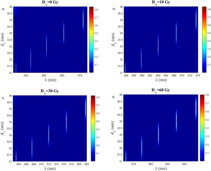
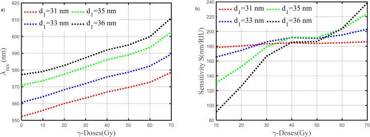
The performance of our suggested gamma-ray radiation sensor will be improved with the help of the optimization approach which describe in the following figures. To do this, the sensitivity values will be computed using the different design parameters, such as the thicknesses of the first, the second, and the defect layers. So, the geometrical parameters are studied to maximize the resonance wavelength (defect mode) shift and, consequently, the sensor sensitivity at various γ-ray radiation doses. Fig. 6a–d show the effect of the thickness of the first layer PSi1 on the resonance wavelength. While the other parameters remain constant, the impact of the thickness of the first layer PSi1 with values of (31, 33, 35, and 36 nm) at various doses (0, 10, 30, and 60 Gy) will be studied. We note that, at the same γ-dose, the position of resonance wavelength shifts to a higher wavelength with an increase in the thickness of the first layer. Eg; At γ-dose is equal (0 Gy), with an increase of d1 (31, 33, 35, and 36 nm), the values of (λres) will be (552.227, 560.718, 570.939, and 577.361 nm), respectively. Also, Fig. 6b– d give the same behavior as Fig. 6a, but at different γ-doses. These figures show that the value of (λres) increases with increasing the value of γ-doses at the same thickness as the first layer. Fig. 7a, show the resonance wavelength versus the doses of γ-ray radiation from (0 to 70 Gy) at different thicknesses of the first layer. Also, Fig. 7b, shows the sensitivity of our sensor versus the doses of γ-ray radiation from (0 to 70 Gy) at different thicknesses of the first layer. Based on this study, we choose the thickness of the first layer with a value of 31 nm as the optimum value for our sensor. Because of this value give sensitivity with very high stability along applied γ-ray radiation. So, this value will be fixed in all subsequent studies.
Fig. 6. The resonance wavelength at different thicknesses of the first layer at, (a) Dγ = 0 Gy, (b) Dγ = 10 Gy, (c) Dγ = 30, and (d) Dγ = 60 Gy. Where, d2 = 73 nm, d3 = 285 nm N1 = N2 = 17, and porosity P1 = 30%, P2 = 80%.
Fig. 7. (a and b) Variation in the resonance wavelength and the sensitivity of our sensor as a function of γ-ray doses from (0 to 70 Gy) at different thicknesses of the first layer, respectively.
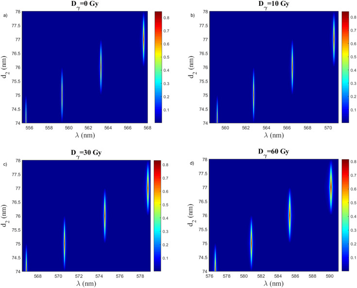
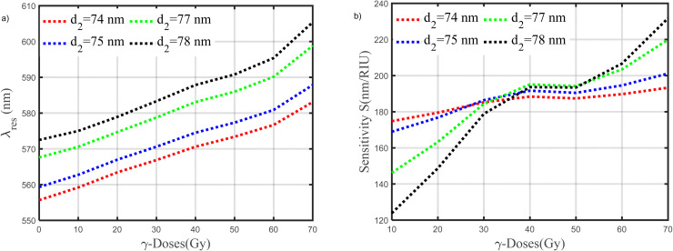
The effect of the thickness of the second layer on the resonance wavelength is demonstrated in Fig. 8a–d. These figures give the same behavior as the previous figures which describe the effect of the thickness of the first layer. The difference concludes in the maximization of the position of the resonance wavelength at each thickness of the second layer compared to the thickness of the first layer, this leads to enhancing the sensitivity of our sensor and other performance parameters. For more details, Fig. 9a, shows the behavior of the resonance wavelength versus the doses of γ-ray radiation from (0 to 70 Gy) at different thicknesses of the second layer. Fig. 9b, demonstrated the sensitivity of our sensor. We note that the sensitivity increases with increasing the thickness of the second layer along with applied γ-ray radiation. Based on this figure, we chose the thickness of the second layer with a value of 75 nm as the optimum value for our sensor. Because of this value give sensitivity with high stability compared to other values, along with applied γ-ray radiation.
Fig. 8. The resonance wavelength at different thicknesses of the second layer at, (a) Dγ = 0 Gy, (b) Dγ = 10 Gy, (c) Dγ = 30, and (d) Dγ = 60 Gy. Where, d1 = 31 nm, d3 = 285 nm N1 = N2 = 17, and porosity P1 = 30%, P2 = 80%.
Fig. 9. (a and b) Variation in the resonance wavelength and the sensitivity of our sensor as a function of γ-ray doses from (0 to 70 Gy) at different thicknesses of the second layer, respectively.
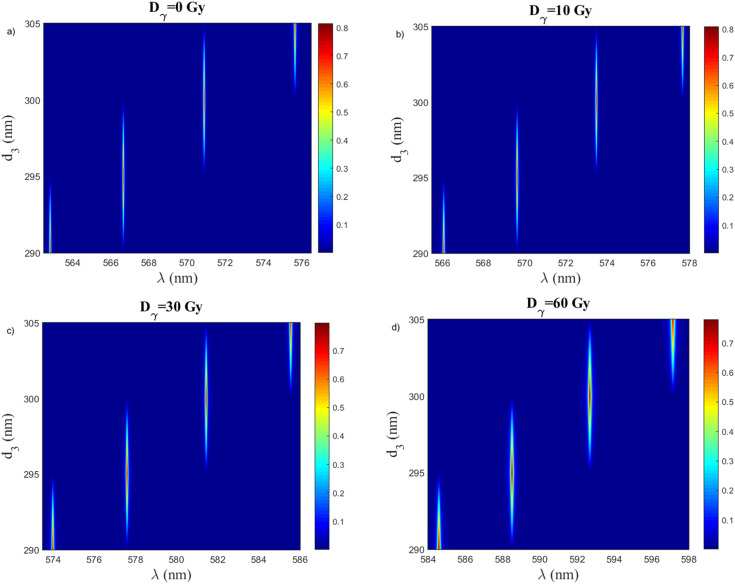
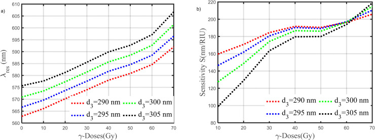
The effect of defect layer thickness to maximize the resonance wavelength shift and improved sensitivity is shown in Fig. 10, and 11. Fig. 10a– d demonstrated the effect of the defect layer thickness on the resonance wavelength. This study is under the optimum previous values. As shown in Fig. 10a–d, with an increase in the thickness of the defect layer the resonance wavelength shift to a higher value along applied different doses of γ-ray radiation. Fig. 11a, and b show the variation in the resonance wavelength and the sensitivity of our sensor as a function of γ-ray doses from (0 to 70 Gy) at different thicknesses of the defect layer, respectively. Based on these results, 290 nm should be the optimal value for the defect layer thickness.
Fig. 10. The resonance wavelength at different thicknesses of the defect layer at, (a) Dγ = 0 Gy, (b) Dγ = 10 Gy, (c) Dγ = 30, and (d) Dγ = 60 Gy. Where, d1 = 31 nm, d2 = 75 nm N1 = N2 = 17, and porosity P1 = 30%, P2 = 80%.
Fig. 11. (a and b) Variation in the resonance wavelength and the sensitivity of our sensor as a function of γ-ray doses from (0 to 70 Gy) at different thicknesses of the defect layer, respectively.
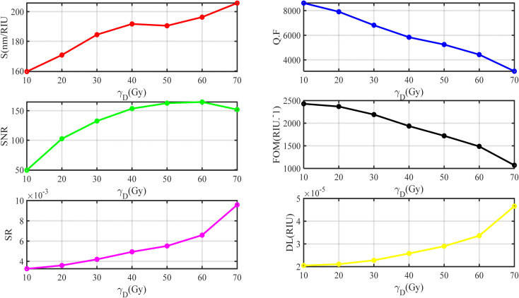
Based on the above findings, the final performance parameters of our sensor are demonstrated at different γ-ray radiation in Fig. 12. The higher value of the sensitivity is 205.790 (nm RIU−1) at γD = 70 Gy. Where the value of sensitivity increases with increasing the doses of γ-ray radiation. This sensor also has a detection limit in the range of (2–5) ×10−5 for the γ-ray radiation range of (0–70 Gy), which is a crucial parameter indicating how the sensor can detect the smallest changes in doses of γ-ray radiation. The sensor's excellent resolution of all resonance wavelengths for any doses of γ-ray radiation is also indicated by the sensor's low FWHM values (less than 0.1922 nm), which are low values that suggest the sensor has a very good resolution (Fig. 12). Moreover, QF is found to decrease with increasing doses of γ-ray radiation but remains as high as 8615.966. Finally, we highlight this high performance in Table 4. When comparing Table 4 with Table 3, we found how the geometric parameters improved the performance parameters of our sensor. The linear fitting of the performance parameters after optimization can be given according to the following equations:
| S = −1.0737 × 10⁻⁶D5γ + 0.000234D4γ − 0.01866D3γ + 0.65011D2γ − 8.5398Dγ + 196.47 | 14 |
| SNR = 2.0896 × 10⁻⁷D5γ − 6.1066 × 10⁻⁵D4γ + 0.0064661D3γ − 0.36379D2γ + 12.53Dγ − 45.433 | 15 |
| SR = 2.4924 × 10⁻⁹D4γ − 3.4323 × 10⁻⁷D3γ + 1.67 × 10⁻⁵D2γ − 0.00027176Dγ+0.0046486 | 16 |
| DL = 9.4697 × 10⁻¹²D4γ − 1.3096 × 10⁻⁹D3γ + 6.63 × 10⁻⁸D2γ − 1.1977 × 10⁻⁶Dγ + 2.71 × 10⁻⁵ | 17 |
| FOM = −7.6129 × 10⁻⁶D5γ + 0.001159D4γ − 0.054938 = D3γ + 0.45096D2γ + 4.0757Dγ + 2387.2 | 18 |
| Q. F = 2.581 × 10⁻⁶D6γ − 0.00059D5γ +0.0525D4γ − 2.1889D3γ + 44.135D2γ − 481.17Dγ + 10735 | 19 |
Fig. 12. The final performance of our sensor.
The final optimum performance parameters are summarized in this table.
| D (Gy) | λ res (nm) | Intensity of λres % | Δλres (nm) | Δλ1/2 (nm) | S (nm RIU−1) | Q. F | SNR | DL (RIU) | SR | FOM (RIU−1) | n (d) | Δ n(d) |
|---|---|---|---|---|---|---|---|---|---|---|---|---|
| 0 | 562.829 | 0.81564 | — | 0.060 | — | 9380.483 | — | — | — | — | 2.2580 | — |
| 10 | 566.069 | 0.8106 | 3.24 | 0.0657 | 159.6059 | 8615.966 | 49.315 | 2.05 × 10⁻⁵ | 3.27 × 10⁻³ | 2429.31 | 2.2783 | 0.0203 |
| 20 | 570.2238 | 0.80403 | 7.3948 | 0.0721 | 170.7806 | 7908.790 | 102.56 | 2.11 × 10⁻⁵ | 3.60 × 10⁻³ | 2368.66 | 2.3013 | 0.0433 |
| 30 | 573.9897 | 0.7979 | 11.1607 | 0.0842 | 184.4743 | 6816.979 | 132.54 | 2.28 × 10⁻⁵ | 4.20 × 10⁻³ | 2190.90 | 2.3185 | 0.0605 |
| 40 | 578.031 | 0.79138 | 15.202 | 0.099 | 191.7023 | 5838.696 | 153.55 | 2.58 × 10⁻⁵ | 4.94 × 10⁻³ | 1936.38 | 2.3373 | 0.0793 |
| 50 | 580.8495 | 0.78672 | 18.0205 | 0.1107 | 190.4915 | 5247.059 | 162.78 | 2.90 × 10⁻⁵ | 5.52 × 10⁻³ | 1720.79 | 2.3526 | 0.0946 |
| 60 | 584.5780 | 0.78047 | 21.749 | 0.132 | 196.2906 | 4428.621 | 164.76 | 3.36 × 10⁻⁵ | 6.59 × 10⁻³ | 1487.05 | 2.3688 | 0.1108 |
| 70 | 592.0307 | 0.7677 | 29.2017 | 0.1922 | 205.7906 | 3080.284 | 151.93 | 4.66 × 10⁻⁵ | 9.58 × 10⁻³ | 1070.71 | 2.3999 | 0.1419 |
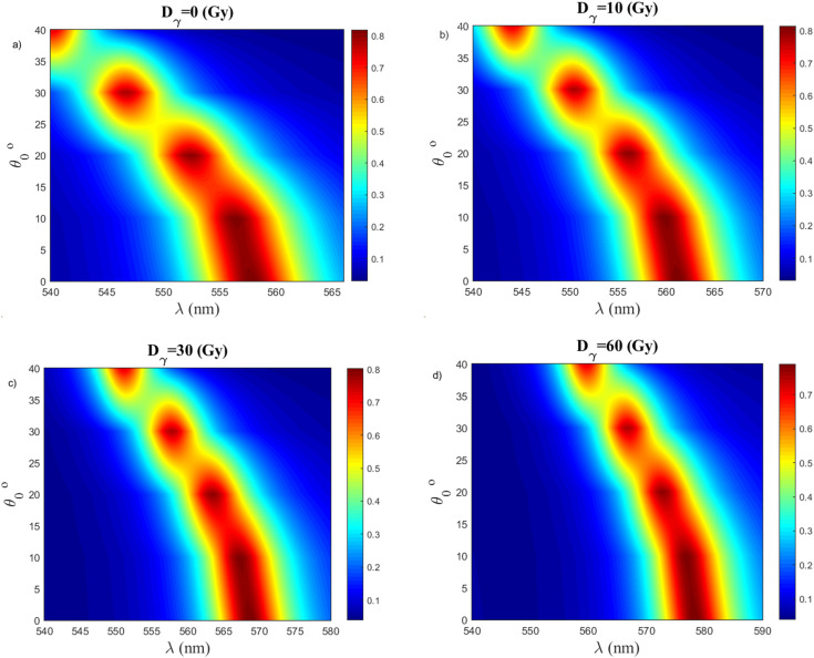
In the following, we study how the resonance wavelength is affected by the angle of incidence and the porosity of two PSi layers. In addition, we explain why we used the values that we specified in Table 1. The angle of incidence as a function of the wavelength at different doses of γ-ray radiation is studied in Fig. 13a–d. Bragg-Snell law can be used to describe the impact of adjusting the incidence angle on the location of the resonance wavelength.53Fig. 13a, it can be observed that with an increase in the value of the incidence angle, the resonance wavelength shifts gradually to the lower wavelength at the same dose of γ-ray radiation. Ex; At γ-dose is equal (0 Gy), with an increase of θo (0°, 10°, 20°, and 30°), the values of (λres) will be (562.828, 561.271, 556.980, and 550.857 nm), respectively. Also, Fig. 13b–d give the same behavior as Fig. 13a, but at different γ-doses. These figures show that the value of (λres) increases with increasing the value of γ-doses at the same incidence angle. We found the decreasing in the shift of the resonance wavelength lead to decreasing the value of sensitivity and other performance parameters according to eqn (8)–(13).
Fig. 13. The effect of incidence angle on resonance wavelength at, (a) Dγ = 0 Gy, (b) Dγ = 10 Gy, (c) Dγ = 30, and (d) Dγ = 60 Gy. Where, d1 = 31 nm, d2 = 73 nm, d3 = 290 nm N1 = N2 = 17, and porosity P1 = 30%, P2 = 80%.
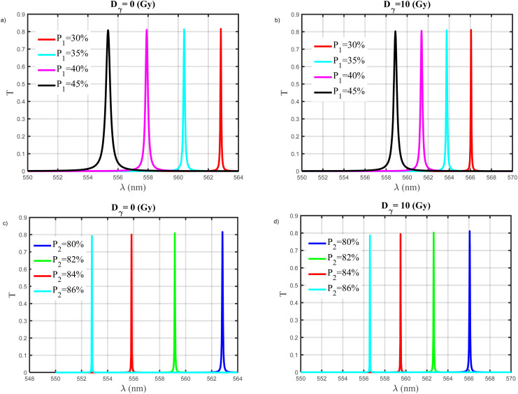
Fig. 14a–d show the effect of the porosity of the first and the second PSi layers on the resonance wavelength. Where the other parameters equal d1 = 31 nm, d2 = 75 nm, d3 = 290 nm, and we consider the case of normal incidence. Fig. 14a and b, show the impact of the porosity of the first PSi-layer with values of (30, 35, 40, and 45%) at various doses (0, and 10 Gy). We note that, at the same γ-dose, the position of resonance wavelength shifts to a lower wavelength with an increase in the porosity of the first PSi-layer. Eg; At γ-dose is equal to (0 Gy) in Fig. 14a, with an increase of P1 (30, 35, 40, and 45%), the values of (λres) will be (562.829, 560.460, 557.882, and 555.442 nm), respectively. In addition, the full width at half the maximum of the resonance wavelength (λ1/2) increase with an increase in the porosity of the first PSi layer. This indicates to the sensitivity of our sensor decrease by increasing the porosity of the first PSi-layer according to eqn (8). Fig. 14c, and d, show the impact of the porosity of the second PSi-layer with values of (80, 82, 84, and 86%) at various doses (0, and10 Gy). Also, Fig. 14c, and d, give the same behavior as Fig. 14a, and b. According to this behavior, we choose the porosity of the first and the second PSi-layers with a value of 30%, and 80% as the optimum value for our sensor. Because of this values give a high sensitivity with excellent resolution for our sensor. For this reason, we mentioned at the beginning of the study that the porosity of the first and the second PSi-layers with values of 30%, and 80%.
Fig. 14. (a and b) The effect of the porosity of the first layer on resonance wavelength at, Dγ = 0 Gy, and Dγ = 10 Gy, respectively. (c and d) The effect of the porosity of the second layer on resonance wavelength at, Dγ = 0 Gy, and Dγ = 10 Gy, respectively.
Finally, we contrast the performance of the suggested sensor with earlier works.8,24,27,54 Compared to other common and more complex structures as shown in Table 5, we believe that our designed structure could be of valuable interest to the radiation communities as a simple, safe, and sensitive tool. Due to a significant contribution that has been devoted towards the fabrication of such devices. Meanwhile, the experimental verifications of the 1D PhCs attracted the attention of many researchers.55–58 In particular, the performance of such a designed sensor is mainly dependent on the control of the constituent of the thicknesses of the layers. In addition, the utilization of PSi through the 1D PhCs for sensing purposes is experimentally demonstrated.59 Caroselli et al. fabricated a microcavity from PSi between two Bragg mirrors for sensing applications based on the electrochemical etching method.59
A detailed comparison between our design and some earlier radiation dosimeters.
| Ref. | Sensitivity as present in paper | Based on | Type of paper |
|---|---|---|---|
| 60 | 9.56 and, 12.67 pm/C | The effect of grating fabrication on the FBGs' radiation sensitivity | Experimental |
| 27 | None | The possibility for employing gamma-irradiated PVA/AgNO3 films in many electrical and semiconductor applications | Experimental |
| 61 | None | The pure-silica-core photonic crystal fibres' (PSC-PCFs') steady-state gamma-ray radiation response under a cumulative dosage of 500 Gy and a dose rate of 2.38 Gy min−1 | Experimental |
| 62 | None | The creation of porous silicon multilayers after gamma/ion irradiating silicon to create tunable distributed bragg reflectors (DBRs) | Experimental |
| 63 | None | The infiltration one-dimensional (1-D) porous silicon photonic crystals (PS-PhCs) with a green-emitting commercial luminescent polymer | Experimental |
| 8 | 10 pm/C at 1550 nm | Optical fiber bragg grating sensors for gamma ray radiation | Experimental |
| 64 | 150 (nm RIU−1) | 2D-PhC for the detection of gamma-ray doses | Theoretical |
| 27 | None | Effects of additive and gamma irradiation on the structural and optical properties of the PVA\AgNO3 films | Experimental |
| This work | 205.7906 nm RIU−1 | The doped PVA-polymer based on 1D-DPhC sensor for the detection of gamma-ray doses | Theoretical |
Conclusion
The doped PVA-polymer based on 1D-DPhC sensor for the detection of γ-ray radiation in the visible range was designed for the first time. The sensing mechanism of this sensor is based on porous silicon and a doped PVA-polymer that infiltrates its pores. Once the sensor is exposed to γ-rays, the optical properties of the doped PVA-polymer will change, and therefore the optical properties of the porous silicon will change, and this is reflected on the transmittance spectrum and resonance wavelength of our sensor. By fitting the experimental data of the doped PVA-polymer, the Bruggeman's effective medium equation of PSi-layer, and the transfer matrix method for calculating the optical characteristics of the dosimeter structure, the theoretical analysis is studied. The numerical results indicated that the PSi-layers changed the doped PVA-refractive polymer's index. Additionally, they demonstrated how this radiation sensor works by showing how the resonance wavelength shifts when it is exposed to gamma rays. It was also examined how the PSi-layer thickness influences performance in order to achieve the highest sensitivity. In addition, the effect of incidence angle on the defect mode. We also explained why we used the values of the porosity of the two PSi-layers and their effect on the defect mode. The unique feature of this paper is that, when exposed to gamma-ray doses ranging from 0 to 70 Gy, the radiation sensor design obtained a high sensitivity of 205.7906 nm RIU−1 in the visible region. In addition, quality factor, signal-to-noise ratio, detection limit, sensor resolution, and figure of merit that have been obtained are 9380.483, ≈49.315, ≈2.05 × 10⁻⁵ RIU, ≈3.27 × 10⁻⁵, and 2429.31 RIU−1, respectively.
Data availability
The datasets used and/or analyzed during the current study are available from the corresponding author on reasonable request.
Author contributions
F. S. conceived the designs. A. H. A., F. S., H. E., A. M. and M. E. designed and conducted the analyses. F. S., H. E, A. M conducted software. F. S, A. H. A., H. E., A. M. and M. E. analyzed the results. All authors reviewed the manuscript.
Conflicts of interest
The authors declare no competing interests.
Supplementary Material
References
- Antar E. M. Effect of γ-ray on optical characteristics of dyed PVA films. J. Radiat. Res. Appl. Sci. 2014;7:129–134. [Google Scholar]
- Cooper W. J., Curry R. D. and O'Shea K. E., Environmental applications of ionizing radiation, John Wiley & Sons, 1998 [Google Scholar]
- Pushpavanam K. Narayanan E. Rege K. Molecular and nanoscale sensors for detecting ionizing radiation in radiotherapy. ChemNanoMat. 2016;2(5):385–395. [Google Scholar]
- Chmielewska D., Radiation methods and uses in nanotechnology. Applications of Ionizing Radiation in Materials Processing, eds Sun Y. and Chmielewski A. G., 2017, pp. 395–414 [Google Scholar]
- Erramli H. and El Asri J., Gamma rays: applications in environmental gamma dosimetry and determination samples gamma-activities induced by neutrons, Use of Gamma Radiation Techniques in Peaceful Applications, 2019, vol. 109 [Google Scholar]
- McLaughlin W., et al., Dosimetry for radiation processing, 1989 [Google Scholar]
- Bashir E. A. A., Synthesis and Optimization of Polymer Film Detector (PVACu2O) in Radiation Therapy, Sudan University of Science and Technology, 2018 [Google Scholar]
- Baccini D., et al., Gamma irradiation response in photonic crystal and standard optical fiber Bragg grating sensors for radiation dosimetry, in AOS Australian Conference on Optical Fibre Technology (ACOFT) and Australian Conference on Optics, Lasers, and Spectroscopy (ACOLS) 2019, International Society for Optics and Photonics, 2019 [Google Scholar]
- Aly A. H. Mehaney A. Eissa M. F. Ionizing particle detection based on phononic crystals. J. Appl. Phys. 2015;118(6):064502. [Google Scholar]
- Rozaila Z. S. et al., Ge and B doped collapsed photonic crystal optical fibre, a potential TLD material for low dose measurements. Radiat. Phys. Chem. 2016;126:9–13. [Google Scholar]
- Ali Omer M. A. Ali Bashir E. A. Synthesis of polyvinyl alcohol and cuprous oxide (PVA/Cu2O) films for radiation detection and personal dosimeter based on optical properties. J. Radiat. Res. Appl. Sci. 2018;11(3):237–241. [Google Scholar]
- Afifi M. et al., Dosimetric impact of some gamma radiation-induced polymeric materials incorporated silicate using thermoluminescence and ultrasonic techniques. Silicon. 2021:1–10. [Google Scholar]
- O’Keeffe S. et al., A review of optical fibre radiation dosimeters. Sens. Rev. 2008;28(2):136–142. [Google Scholar]
- Avino S. et al., Ionizing radiation detectors based on Ge-doped optical fibers inserted in resonant cavities. Sensors. 2015;15(2):4242–4252. doi: 10.3390/s150204242. [DOI] [PMC free article] [PubMed] [Google Scholar]
- Berghmans F. and Gusarov A., Fiber Bragg grating sensors in nuclear environments .Fiber Bragg grating sensors: recent advancements, industrial applications and market exploitation, 2011, pp. 218–237 [Google Scholar]
- Morante M., Fiber Bragg Grating sensors for harsh environments, 2018 [DOI] [PMC free article] [PubMed] [Google Scholar]
- Mehaney A., Elsayed H. A. and Ahmed A. M., Detection of isoprene traces in exhaled breath by using photonic crystals as a biomarker for chronic liver fibrosis disease, 2021 [Google Scholar]
- Abadla M. M. Elsayed H. A. Mehaney A. Thermo-optical properties of binary one dimensional annular photonic crystal including temperature dependent constituents. Phys. E. 2020;119:114020. [Google Scholar]
- Haberko J. Froufe-Pérez L. S. Scheffold F. Transition from light diffusion to localization in three-dimensional amorphous dielectric networks near the band edge. Nat. Commun. 2020;11(1):1–9. doi: 10.1038/s41467-020-18571-w. [DOI] [PMC free article] [PubMed] [Google Scholar]
- Elsayed H. A. Mehaney A. Theoretical verification of photonic crystals sensor for biodiesel detection and sensing. Phys. Scr. 2020;95(8):085507. [Google Scholar]
- Ahmed A. M. Mehaney A. Ultra-high sensitive 1D porous silicon photonic crystal sensor based on the coupling of Tamm/Fano resonances in the mid-infrared region. Sci. Rep. 2019;9(1):1–9. doi: 10.1038/s41598-019-43440-y. [DOI] [PMC free article] [PubMed] [Google Scholar]
- Chiappini A. et al., Photonic crystal stimuli-responsive chromatic sensors: a short review. Micromachines. 2020;11(3):290. doi: 10.3390/mi11030290. [DOI] [PMC free article] [PubMed] [Google Scholar]
- Sporea D., et al., Optical fibers and optical fiber sensors used in radiation monitoring, 2012 [Google Scholar]
- Raghuvanshi S. et al., Effect of gamma irradiation on the optical properties of UHMWPE (Ultra-high-molecular-weight-polyethylene) polymer. Nucl. Instrum. Methods Phys. Res., Sect. B. 2012;271:44–47. [Google Scholar]
- Chandrappa H. et al., Physico-chemical properties of PVA-Nile blue (C20H20ClN3O) polymer composite structures for γ-ray protection: A comparative γ-ray irradiation studies. Radiat. Phys. Chem. 2021;184:109481. [Google Scholar]
- Mir F. A. Gani A. Asokan K. Gamma irradiation studies of composite thin films of poly vinyl alcohol and coumarin. RSC Adv. 2016;6(2):1554–1561. [Google Scholar]
- Osman I. M. et al., Effects of additive and gamma irradiation on the structural and optical properties of polyvinyl alcohol doped with silver nitrate. Glob. Sci. J. 2021;9(6):2054–2062. [Google Scholar]
- Yue X. et al., Porous silicon photonic crystal/silver composite produced by microwave-assisted reduction: applications to surface-enhanced Raman scattering. Opt. Mater.: X. 2019;2:100027. [Google Scholar]
- Zaky Z. A. Sharma A. Aly A. H. Tamm plasmon polariton as refractive index sensor excited by gyroid metals/porous Ta2O5 photonic crystal. Plasmonics. 2022;17(2):681–691. [Google Scholar]
- Harraz F. A. Porous silicon chemical sensors and biosensors: A review. Sens. Actuators, B. 2014;202:897–912. [Google Scholar]
- Levitsky I. A. Porous silicon structures as optical gas sensors. Sensors. 2015;15(8):19968–19991. doi: 10.3390/s150819968. [DOI] [PMC free article] [PubMed] [Google Scholar]
- Zhong F. et al., Optical characteristics of porous silicon photonic crystals prepared on the back surface of silicon wafers. Optik. 2020;201:163486. [Google Scholar]
- Vincent G. Optical properties of porous silicon superlattices. Appl. Phys. Lett. 1994;64(18):2367–2369. [Google Scholar]
- Salem M. et al., Electrochemical stabilization of porous silicon multilayers for sensing various chemical compounds. J. Appl. Phys. 2006;100(8):083520. [Google Scholar]
- Zhang H. et al., Optical nose based on porous silicon photonic crystal infiltrated with ionic liquids. Anal. Chim. Acta. 2017;953:71–78. doi: 10.1016/j.aca.2016.11.053. [DOI] [PubMed] [Google Scholar]
- Aly A. H. Sayed F. A. THz cutoff frequency and multifunction Ti2 Ba2 Ca2 Cu3 O1 0/G a A s photonic bandgap materials. Int. J. Mod. Phys. B. 2020;34(10):2050091. [Google Scholar]
- Maeno K. et al., Polymer-based photonic crystal cavity sensor for optical detection in the visible wavelength region. Anal. Sci. 2016;32(1):117–120. doi: 10.2116/analsci.32.117. [DOI] [PubMed] [Google Scholar]
- Caruso R. A. Susha A. Caruso F. Multilayered titania, silica, and laponite nanoparticle coatings on polystyrene colloidal templates and resulting inorganic hollow spheres. Chem. Mater. 2001;13(2):400–409. [Google Scholar]
- Wang G. et al., One-dimensional alumina photonic crystals with a narrow band gap and their applications to high-sensitivity concentration sensor and photoluminescence enhancement. Superlattices Microstruct. 2015;86:546–551. [Google Scholar]
- Yan P. et al., Fabrication of one-dimensional alumina photonic crystals with a narrow band gap and their application to high-sensitivity sensors. J. Mater. Chem. C. 2013;1(8):1659–1664. [Google Scholar]
- Zhong K. et al., Defect mode passband lasing in self-assembled photonic crystal. ACS Photonics. 2016;3(12):2330–2337. [Google Scholar]
- Kennedy S. R. et al., Fabrication of tetragonal square spiral photonic crystals. Nano Lett. 2002;2(1):59–62. [Google Scholar]
- Sayed F. A. Elsayed H. A. Aly A. H. Optical properties of photonic crystals based on graphene nanocomposite within visible and IR wavelengths. Opt. Quantum Electron. 2020;52(10):1–16. [Google Scholar]
- Aly A. H. et al., MATLAB Simulation-Based Theoretical Study for Detection of a Wide Range of Pathogens Using 1D Defective Photonic Structure. Crystals. 2022;12(2):220. [Google Scholar]
- Tammam M., et al., Defected photonic crystal array using porous GaN as malaria sensor, in IOP Conference Series: Materials Science and Engineering, IOP Publishing, 2021 [Google Scholar]
- Mehaney A. Ahmed A. M. Locally resonant phononic crystals at low frequencies based on porous SiC multilayer. Sci. Rep. 2019;9(1):1–12. doi: 10.1038/s41598-019-51329-z. [DOI] [PMC free article] [PubMed] [Google Scholar]
- Sabra W. et al., Numerical optimization of 1D superconductor photonic crystals pressure sensor for low temperatures applications. Solid State Commun. 2022:114671. [Google Scholar]
- Du Q. et al., Gamma radiation effects in amorphous silicon and silicon nitride photonic devices. Opt. Lett. 2017;42(3):587–590. doi: 10.1364/OL.42.000587. [DOI] [PubMed] [Google Scholar]
- Cai W. et al., Gamma-radiation effects in pure-silica-core photonic crystal fiber. Chin. Phys. B. 2017;26(11):114211. [Google Scholar]
- Cocorullo G. et al., Measurement of the thermo-optic coefficient of a-Si: H at the wavelength of 1500 nm from room temperature to 200 °C. J. Non-Cryst. Solids. 2002;299:310–313. [Google Scholar]
- Ibrahim M. S. S. et al., Highly sensitive photonic crystal gamma ray dosimeter. Opt. Quantum Electron. 2021;53(7):1–19. [Google Scholar]
- El-Fiki S. et al., Investigation of the effect of gamma rays on optical properties of polymers. Radiat. Phys. Chem. 1996;47(5):761–764. [Google Scholar]
- Aly A. H. Elsayed H. A. Defect mode properties in a one-dimensional photonic crystal. Phys. B. 2012;407(1):120–125. [Google Scholar]
- Canning J., et al., Gamma irradiation effects in photonic crystal fibre Bragg gratings, in Australian Institute of Physics (AIP) Congress, 2018 [Google Scholar]
- Shen H. et al., One-dimensional photonic crystals: fabrication, responsiveness and emerging applications in 3D construction. RSC Adv. 2016;6(6):4505–4520. [Google Scholar]
- González-García L. et al., Single-step fabrication process of 1-D photonic crystals coupled to nanocolumnar TiO 2 layers to improve DSC efficiency. Opt. Express. 2015;23(24):A1642–A1650. doi: 10.1364/OE.23.0A1642. [DOI] [PubMed] [Google Scholar]
- Shaban M. et al., Tunability and sensing properties of plasmonic/1D photonic crystal. Sci. Rep. 2017;7(1):1–10. doi: 10.1038/srep41983. [DOI] [PMC free article] [PubMed] [Google Scholar]
- Fukukawa K.-i. Ueda M. Recent progress of photosensitive polyimides. Polym. J. 2008;40(4):281–296. [Google Scholar]
- Caroselli R. et al., Real-time and in-flow sensing using a high sensitivity porous silicon microcavity-based sensor. Sensors. 2017;17(12):2813. doi: 10.3390/s17122813. [DOI] [PMC free article] [PubMed] [Google Scholar]
- Lin S. et al., Effect of grating fabrication on radiation sensitivity of fiber Bragg gratings in gamma radiation field. IEEE Trans. Nucl. Sci. 2011;58(4):2111–2117. [Google Scholar]
- Entezam A. et al., Thermoluminescence response of Ge-doped cylindrical-, flat-and photonic crystal silica-fibres to electron and photon radiation. PLoS One. 2016;11(5):e0153913. doi: 10.1371/journal.pone.0153913. [DOI] [PMC free article] [PubMed] [Google Scholar]
- Vendamani V. et al., Fabrication of porous silicon based tunable distributed Bragg reflectors by anodic etching of irradiated silicon. Nucl. Instrum. Methods Phys. Res., Sect. B. 2015;358:105–111. [Google Scholar]
- Robbiano V. et al., C-Si hybrid photonic structures by full infiltration of conjugated polymers into porous silicon rugate filters. Nanomater. Nanotechnol. 2018;8:1847980418788404. [Google Scholar]
- Ibrahim M. S. S. Hamed M. K. G. El-Okr M. M. Highly sensitive photonic crystal gamma ray dosimeter. Opt. Quantum Electron. 2021;53:348. [Google Scholar]
Associated Data
This section collects any data citations, data availability statements, or supplementary materials included in this article.
Data Availability Statement
The datasets used and/or analyzed during the current study are available from the corresponding author on reasonable request.


