Abstract
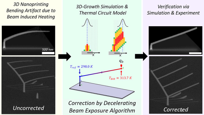
3D nanoprinting, using focused electron beam-induced deposition, is prone to a common structural artifact arising from a temperature gradient that naturally evolves during deposition, extending from the electron beam impact region (BIR) to the substrate. Inelastic electron energy loss drives the Joule heating and surface temperature variations lead to precursor surface concentration variations due, in most part, to temperature-dependent precursor surface desorption. The result is unwanted curvature when prescribing linear segments in 3D objects, and thus, complex geometries contain distortions. Here, an electron dose compensation strategy is presented to offset deleterious heating effects; the Decelerating Beam Exposure Algorithm, or DBEA, which corrects for nanowire bending a priori, during computer-aided design, uses an analytical solution derived from information gleaned from 3D nanoprinting simulations. Electron dose modulation is an ideal solution for artifact correction because variations in electron dose have no influence on temperature. Thus, the generalized compensation strategy revealed here will help advance 3D nanoscale printing fidelity for focused electron beam-induced deposition.
Introduction
Additive manufacturing of three-dimensional objects on the micro- and nanoscale is a challenging task but of high interest in research and development. Among the possible fabrication techniques, only a few allow the direct writing of real 3D structures with feature sizes below 1 μm.1 3D printing at the nanoscale is possible by focused electron beam-induced deposition or FEBID.2 Advantageous in that the method is truly 3D and compatible with extreme surface topographies, the method unfortunately exhibits relatively low material deposition rates.1,3 Fortunately, deposition rates are sufficient to print complex assemblies of nanowires over microscale dimensions,4−8 architectures suitable for sensing,9 actuation,10 and/or micro/nanomachine or metamaterial applications.
In basic FEBID mode, deposition occurs in response to the electron-stimulated dissociation of surface-adsorbed precursor molecules. Experiments are often conducted using the nanoscale electron probe available in a scanning electron microscope. A steady precursor vapor flow is required for continuous deposition. Vacuum requirements for proper scanning electron microscopy (SEM) operation limit the precursor pressure in the chamber to a threshold value to avoid significant gas phase electron scattering, which would otherwise degrade electron probe resolution on the substrate surface. This factor contributes in part to a relatively low deposition rate. The deposition rate is also negatively influenced by the relatively low probability of electron-stimulated precursor dissociation; most chemistries currently used were developed for thermal decomposition, not electron-stimulated dissociation.11,12
In 3D nanoprinting FEBID mode, linear beam scanning is introduced in the 2D focal plane, which translates into 3D deposition; a nanowire effectively “lifts off” the substrate surface at an initial inclination angle (ζ). Inclined nanowires spanning 0° < ζ < 90° are defined as “segments” and ζ as the “segment angle”. The other deposition element relevant to mesh object deposition, the “pillar”, is simply a vertical nanowire (ζ = 90°). Importantly, ζ is determined by the beam speed and, conveniently, FEBID spans the full range of inclination of ζ = 0–90°, i.e., horizontal to vertical. While the focus of our work is on 3D nanostructuring restricted to positive inclination angles, we note that researchers have observed negative13,14 and multibranching phenomena in both metals and oxide FEBID deposits.15 Even more complex mesh object models, consisting of interconnected networks of linear nanowires, may be deposited by assigning a series of sequential linear scans in the 2D focal plane.4 However, complex nanowire network models require careful exposure design because the translation of 2D scanning to 3D deposition depends on continuous electron beam/deposit overlap. If the beam becomes disengaged from the deposit during growth, no dynamic feedback currently exists to correct and re-establish deposition. This explains the variety of CAD/exposure software reported in the literature to facilitate 3D nanoprinting.4,7,16−19
Future demonstrations of sensing, actuation, and MEMS/NEMS are expected to benefit from the variety of 3D geometries accessible using FEBID 3D nanoprinting. Demonstrations of complex 3D nanoprinting, such as provided in ref (6), were impossible prior to the development of FEBID.1 These advancements in 3D FEBID enabled actual applications such as advanced scanning probe tips,9,20 magnetic 3D geometries,21−24 and plasmonic 3D structures.6,25,26 Ultimately, complex deposits supporting future applications will require even increasing levels of nanoscale precision and reproducibility, across a broad range of 3D meshes, to make a demonstrative and broad impact. Currently, this is a challenge because, for the most popular precursor gases, e.g., MeCpPtMe3, Me2Au(acac), and W(CO)6, used during FEBID, deposition occurs under conditions of variable precursor surface concentration in the beam impact region (BIR), leading to a variable deposition rate.27 Deposition precision and reproducibility are difficult to maintain under such variable conditions degrading predictability and complicating exposure design.
Specifically, precursor surface concentration gradients develop on the deposit surface during FEBID due to two key factors. First, in the BIR, a precursor-limited reaction (PLR) develops during FEBID because the vacuum condition limits the precursor surface impingement rate to a magnitude that is insufficient to sustain a constant precursor surface concentration under electron irradiation, even considering the relatively low electron impact precursor dissociation probability. This is the first factor that causes a precursor surface concentration gradient. The second factor is related to the magnitude of the electron beam current required to drive deposition.
The electron beam current required to sustain practical deposition rates leads to beam-induced heating in the deposit. Transmitted primary electron trajectories experience inelastic scattering inside the deposit volume, and a fraction of the deposited electron energy decays as thermal energy in the deposit. A temperature gradient develops over the length of the deposit as the deposited thermal energy is transferred to the lower temperature substrate. Ultimately, the surface concentration changes, in this case, along the entire length of the deposit, due to the temperature-dependent nature of precursor molecule surface attachment. One option to counteract the thermally induced desorption is cooling the substrate. For example, cryogenic substrate conditions can significantly enhance the growth rates;28 however, with condensed precursor layers, no real 3D FEBID as described here can be realized. Cooling the substrate but keeping the temperature above the precursor condensation point indeed results in an increased 3D growth rate with almost no loss of printing quality.29 Nevertheless, the beam-induced heating effects and the presented compensation strategy in this study also apply here, even though with a small offset in temperatures.
Thus, as it currently stands, FEBID is executed under conditions where temporal and spatial gradients in precursor surface concentration preclude an ideal, generalized deposition recipe applicable for all geometries. Thus, unwanted artifacts of deposition evolve, compromising the duplication of the CAD mesh object models, at least for basic patterning strategies such as constant beam speed exposure.8,17
Presented here is a simulation-informed analytical model that anticipates and corrects for segment bending caused by surface variations in precursor surface concentration. The model couples the mathematical physics causing bending to microscopy parameters for electron beam exposure to apply exposure dose variation in patterning files. In this way, it is possible to compensate for deposit bending, a priori in the CAD, to prevent distortions. This approach provides a more generalized framework for precise and reliable 3D nanoprinting. Beyond the practical improvement achieved by this upfront bending correction even for complex 3D geometries, the calculations and simulations presented in this work have revealed deeper insights into the growth dynamics of 3D FEBID. The following background section, which is suitable for both a general audience and FEBID specialists, establishes a common basis for subsequent in-depth discussion.
Before proceeding to the next section, please note that Table 1 provides a list of acronyms used in the current paper, which should help the reader navigate the relatively large number of acronyms included. Also, Supporting Information 1 provides comprehensive lists of experimental and/or simulation parameters for each figure presented, while Supporting Information 2 gives information on experimental calibrations.
Table 1. Acronyms Specific to 3D Nanoprinting by Focused Electron Beam-Induced Deposition.
| parameter | definition |
|---|---|
| FEBID | focused electron beam-induced deposition |
| DBEA | decelerating beam exposure algorithm |
| TCN | thermal circuit network |
| GIS | gas (precursor) injection system |
| EEL | electron energy loss |
| SEM | scanning electron microscopy |
| CAD | computer-aided design |
| PE | primary electron |
| PLR | precursor-limited regime |
| ELR | electron-limited regime |
| BSE | backscatter scattered electron |
| FSE | forward scattered electron |
| SE | secondary electron |
| EIV | electron interaction volume |
| BIR | beam impact region |
| MFP | mean free path |
Background (Physics)
Problem I: Limitations in Precursor Delivery during FEBID
Stable, repeatable FEBID is best obtained by first establishing an equilibrium surface coverage of precursor molecules on the substrate surface, prior to the electron beam (e– beam On) state. Typically limited to a monolayer, the actual fractional coverage is often lower and depends, in part, on the precursor impingement flux on the substrate surface (Supporting Information 3). A capillary-style gas-injection source, aligned to the BIR, ideally provides a steady-state precursor flux, at least within tens of micrometers surrounding the BIR.30 The use of the capillary also limits gas phase scattering to a region just above the substrate surface. The important consequence of this precursor delivery framework is the development of a steady-state, fractional monolayer coverage of adsorbed precursor molecules on the surface under the e– beam Off state.
Now, consider the e– beam On state in the stationary substrate exposure mode under continuous precursor flow. The influence of the electron–surface interaction on deposition will be described first, followed by a summary of the implications of the electron–volume interaction.
Secondary electrons (SEs) generated and emitted in the near-surface region have the most favorable kinetic energies for molecular dissociation, with small contributions from primary electrons (PEs), forward scattered electrons (FSEs), and backscattered electrons (BSEs).31 Dissociation products containing the deposition species of interest condense and accumulate as deposit under continuous and stationary beam exposure. The SE mean free path (MFP) is nominally several nanometers at most, which limits the spatial extent of deposition to approximately the original PE beam waist in the BIR.
Stationary beam exposure, at least initially, yields the maximum vertical growth rate as newly formed deposit is quickly coated with a fresh precursor, supporting continuous deposition. The fresh precursor arrives either directly from the vapor phase, by the surface diffusion of adsorbed precursor, or a combination of both processes. Unfortunately, this so-called electron-limited growth regime (ELR) persists briefly, if at all, typically on the order of a few nanometers of deposition because the precursor impingement flux is restricted to a threshold value to avoid vapor phase scattering of the primary electron beam in transit to the substrate. Further, not only is (1) the replenishment rate by the vapor source unable to sustain the equilibrium precursor coverage originally established in the e– beam Off state but (2) precursor surface diffusion is also too slow to maintain this equilibrium. In fact, as deposition progresses, a precursor depletion zone develops on the surface around the BIR. As a result, a local/short-range surface precursor concentration gradient develops about the BIR. On the other hand, this phenomenon leads to a relatively lower deposition rate compared to the initial growth experienced when a beam initially arrives at the position with equilibrium gas coverage. On the other hand, the short-range gradient is remarkably stable over the course of nanowire/segment deposition and thus leads to predictably linear growth rates.27
Please note that the precursor impingement flux is not the only factor that determines the absorbed precursor surface concentration and, ultimately, the deposition rate. The precursor surface sticking probability (δ) and mean surface adsorption time (τ) also play a role in dictating the precursor surface concentration, at least for the case of physisorption.
Problem II: Fundamental Limits to the FEBID Deposition Rate
There also exists a fundamental limit to the deposition rate: Even under idealized monolayer precursor coverage, FEBID is orders of magnitude slower than electron beam lithography,32 since the precursor dissociation probability per SE is relatively low. An increase in the deposition rate can be achieved by modest increases in the current while not sacrificing resolution, but the gains are both temporary and self-limiting. They are temporary in that an increase in electron beam current can increase the initial deposition rate, but the rate quickly decreases as significant precursor depletion ensues. Regrettably, they are self-limiting because beam-induced heating also scales with the electron beam current. Penetrating PEs transfer energy to the deposit volume by way of inelastic electron energy loss (EEL), resulting in Joule heating, a natural consequence of the electron–volume interaction. Ultimately, the deposition rate decreases with an increase in deposit temperature, as described next.
Problem III: Simultaneous Electron Beam-Induced Heating
Two unwanted physical processes arise from beam-induced deposit heating. First, the associated temperature rise reduces the precursor surface concentration because precursor surface desorption is thermally activated, i.e., Arrhenius, and increases with temperature. Second, inelastic EEL, which decays as heat to the deposit volume, is concentrated at the BIR during 3D nanoprinting. The beam thus acts as a localized heat source raising the temperature of the BIR. The substrate serves as an idealized heat sink, nominally at room temperature, dissipating the heat from the deposit. A thermal gradient is thus established through the deposit, resulting in the flow of heat from the BIR to the substrate. The precursor surface desorption rate increases with temperature so a spatial variation in the equilibrium precursor surface concentration accompanies the temperature gradient along the deposit surface.
To further complicate matters, electron beam-induced heating effects are significant in the interconnected nanowire mesh objects due to the relatively large thermal resistance of each nanowire constituting the 3D mesh. The nanowire thermal resistance (RT) is significant because the heat flow path length (microscale) is large relative to the mathematical product of cross-sectional area (nanoscale) and deposit thermal conductivity (k) as RT = L/kA. The resulting thermal gradient naturally induces a global/long-range precursor surface concentration gradient that extends along the deposit length. Importantly, this phenomenon frustrates the notion of a generalized framework for 3D nanoprinting because the precursor surface concentration in the BIR ultimately depends on the 3D mesh geometry of the deposit.
Thus, electron-stimulated precursor dissociation (a surface interaction) and beam-induced heating (a volume interaction) lead to the development of local and global precursor surface gradients, respectively, that influence deposition. In summary, the local gradient is driven by the combined effects of beam dissociation and inadequate precursor surface replenishment, while the global gradient is caused by electron beam-induced heating, which depends on the deposit geometry.29 Please also note the influence of the thermal conductivity k of the deposited materials. Since this value can vary with fabrication parameters33 and also for different FEBID materials, the effect of beam-induced heating is more or less pronounced.
The deposition rate at the segment BIR is dictated, in part, by the short-range precursor surface gradient, which is a surprisingly stable feature over the course of nanowire deposition.27 This stability is favorable for approaching linear, and therefore predictable, 3D nanoprinting in simple geometries. Nonetheless, the deposition rate declines steadily over the course of nanowire deposition in mesh object models due to the long-range precursor surface gradient and the steady rise in the BIR temperature with deposit length. This is the primary source of the observed segment bending in mesh object models.16
A decelerating beam exposure algorithm (DBEA) is presented here to compensate for the local and global precursor surface gradients caused by electron beam-induced heating. Using DBEA, the electron beam dwell time per pixel (τd) continuously increases in the scanning path (x′) during nanowire deposition. In the end, dose modulation was the only realistic option for correction because alternative strategies including pressure, beam current, or temperature modulation were either impossible (beam current) or impractical (pressure and temperature).
Consider electron beam current modulation as a potential candidate to correct for a decreasing deposition rate. This approach is counterproductive for mesh objects; although the beam current can in principle increase the deposition rate, this only works in the absence of electron beam heating. The high thermal resistance of mesh objects nullifies this approach; electron beam-induced heating scales with beam current.
These arguments suggest that the best option for a priori structural distortion correction is DBEA and the results presented here further validate the merit of the strategy.
Background (Methods)
3D Nanoprinting
Digital electron beam scanning is implemented during 3D nanoprinting: nominally instantaneous beam displacement to a new exposure pixel follows a stationary exposure period at the current pixel8,17 (Supporting Information 4). The digital beam velocity is defined as
| 1 |
where Λ is the pixel point pitch, i.e., the beam displacement, and τd is the electron beam pixel dwell time. Importantly, the beam velocity controls nanowire inclination with respect to the substrate surface. Again, the segment type of nanowire is characterized by an inclination angle (ζ < 90°). Segment angle variations are imposed by changes in vb, where vb is varied by changing τd while keeping Λ constant. Alternative strategies are reported in the literature.7 As distinct from a segment, a vertical nanowire, or pillar (ζ = 90°), is deposited using relatively long single-pixel, stationary electron beam exposure and grows normal to the primary electron beam trajectory. Pillar elements are prone to a decreasing vertical growth rate as a function of pixel dwell time.34 This is easily accounted for in design using the pillar height versus single-pixel dwell time calibration data provided in the calibration file example in Supporting Information 2.
Please note that in certain cases of relatively long pixel dwell times, multiple pixel “exposures” are required to accumulate the total dose required to satisfy the total pixel “dwell time” due to hardware limitations in patterning. “Exposure” and “dwell” will be used to indicate this difference throughout the paper.
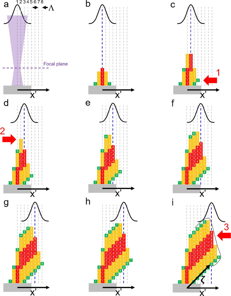
A simple 3D nanoprinting scheme reveals hallmark features of deposition (Figure 1). The beam traces a linear path projection in the focal plane along the x′-coordinate (Supporting Information 4) during segment deposition where each sequential exposure pixel is represented by an integer in the scheme (Figure 1a). The focal plane of the beam is fixed during nanoprinting (Figure 1a, dashed line), typically located tens of nanometers above the surface (Supporting Information 5). The reader is encouraged to review relevant coordinate systems to 3D FEBID nanoprinting (Supporting Information 4).
Figure 1.
3D nanoprinting scheme showing the spatial distribution of deposition as a function of electron beam dwell position (Gaussian, black line). (a) Primary electron beam positions are indicated by integers; Λ is the pixel point pitch. The stationary focal plane is also shown (dashed line). The deposition model consists of numbered voxels cross-referenced to the beam position when they were deposited. Hue indicates the position of the voxel relative to the primary electron beam flux profile when deposited. (c) Direct and proximal deposition convolve to yield deposition features (1 →) favorable for 3D deposition. Here, a ledge feature has developed. (d) The nanowire/segment shape evolves into a complex shape that deviates from the primary electron beam flux profile (2 →). (a–i) A constant digital beam velocity (vb) eventually yields a nearly linear segment with (i) a steady-state tip shape (3 →, gray curving line).
The impinging primary electron beam current flux spatial profile is approximately Gaussian in shape (Figure 1a, black curve). The individual PEs constituting the beam profile enter the surface and generate SEI, which are emitted at a fraction of δI per PE (Supporting Information 6). SEI exit the surface, inducing direct precursor dissociation at the point of surface emission, mostly in the BIR. Thus, the SEI-emitted current flux profile (iSE″) strongly influences the deposition topography (Figure 1b) during stationary pixel exposure; the resulting deposit topography is a convolution of (1) iSE″, (2) the penetration of the electron interaction volume (EIV) into the bulk, (3) the variation in SEI emission as a function of local surface slope, and (4) any changes in precursor surface concentration from point to point on the surface. Regarding (2), the EIV–deposit convolution results in forward and backscattered electrons (FSE and BSE) that may exit the deposit surface, even outside the BIR, generating emitted secondary electrons (SEII) that cause proximity deposition (Figure 1c, 1 →): this combination of both direct and proximal deposition creates topography favorable for nanowire/segment substrate lift-off, which is the true 3D deposition required for nanoprinting.
The 3D nanoprinting scheme illustrates the complex relationship that can develop between the maximum segment height and the PE beam impact position (Figure 1d, 2 →). In the scheme, the maximum height lags the beam impact centerline. This artifact is observed in real experiments.35 The PE energy, current, and beam size have a strong impact on the position of this feature35 and the basic shape of the segment tip. Although overly simplistic, the reader may follow the progress of deposition (Figure 1b–h) to appreciate the (1) evolution of the spatial distribution of deposition per pixel and (2) the development of ζ; deposition culminates in a steady-state segment tip shape and constant inclination (Figure 1i) if only linear growth can be sustained. This is the topic of the current paper.
3D Nanoprinting Calibration
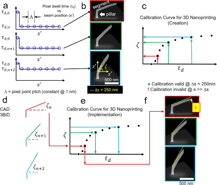
A multitude of mesh object models of acceptable quality may be deposited using a surprisingly simple calibration procedure.17 The procedure consists of depositing an array of calibration structures followed by SEM characterization of ζ to associate ζ and vb. Select CAD will be referred to with capital letters.
A calibration structure consists of a pillar that supports an inclined segment. It is recommended that the segment has a total length of nominally 250 nm for proper calibration (Supporting Information 4). Calibration structures share a common pillar height and constant Λ for segment deposition. vb is varied for each calibration structure using τd. The translation from calibration to deposition is presented schematically in Figure 2. The need for calibration is reviewed in Supporting Information 7.
Figure 2.
Application of 3D nanoprinting calibration procedure for mesh object model definition by CAD. (a) Deposit exposure is defined by a data file containing the electron beam dwell time per pixel versus the position of the electron beam projected in the substrate plane. Pillar element exposure is set by the pillar dwell time (τd,p) and common to all calibration structures. Subsequently, segment exposure ensues using a constant pixel point pitch (Λ) and a constant dwell time (τd); the latter parameters control the segment angle. (b) Simulated SEM images (acquired at 52° with respect to the substrate surface normal) of select simulated calibration structures. The simulations of calibration structure deposition reveal the pillar and segment geometry; the pillar element is aligned along the z′-coordinate, while the segment extends along the x′–z′ plane (Supporting Information 4). The segment angle (ζ) is quantified by measuring the inclination angle of the segment, with respect to the substrate surface, using linear extrapolation to the position Δs = 250 nm as measured from the origin of the segment. (c) Future CAD makes use of an assembled calibration curve expressing ζ(τd). (d) Segment angles are computed from a user-defined mesh object model, and (e) τd’s are assigned to each segment using the calibration curve in inverse as τd(ζ). (f) Unfortunately, replication of the mesh object model structure is recovered only in the limit of relatively short nanowires (≅500 nm) because of segment bending that develops for longer segments. See Supporting Information 1 for deposition parameters.
Pixel dwell time as a function of exposure path τd(x′) defines calibration structure exposure (Figure 2a). Calibration structure deposition begins with a relatively long (order of seconds), single-pixel beam exposure to define the pillar (Figure 2a, τd,p, open circle). Multiple, closely spaced (Λ = 1 nm), and relatively brief (1–100 ms) exposures follow to define the segment exposure element. Across multiple calibration structures, as the dwell time per segment pixel increases, a concomitant increase in ζ is observed as the increased dose per unit length translates into deposit elongation along z′; simulated SEM images of simulations conducted using a primary electron beam energy of 30 keV and a current of 35 pA clearly show the increase in ζ with τd (Figure 2b). Moving forward, this experimental condition (and complementary simulations) will be indicated in shorthand as ⟨E30:i35⟩. A calibration curve is compiled graphically, as in Figure 2c, when a suitable number of data points are generated to approximate the functional relationship ζ(τd); each data point in Figure 2c was derived from the deposition of a unique calibration structure.
Mesh object model computer-aided design (CAD) follows calibration by using the calibration curve in the inverse sense; segment angles are computed for all segments defined in the model (Figure 2d), and the calibration curve is used to interpolate τd based on ζ (Figure 2e). CAD software is available for this purpose.17 Briefly, a mesh object model is defined by simply specifying object vertices and segments. Upon model completion, the mesh object model is submitted for exposure file creation, which consists of (1) assigning the definition of each nanowire as a pillar or segment and (2) the automated interpolation of ζ for each submitted segment to determine the required τd. The resultant exposure file format is compatible with several commercial microscopy platforms.3,8 This method yields CAD replication of acceptable, but imperfect, quality for duplication of simple mesh object models due to segment bending (Figure 2f).
Significant, negative segment deflection/bending occurs nominally 250 nm beyond the segment origin. The bending occurs in the x′–z′ plane in the (−z′) direction, i.e., oriented paraxial to the impinging PE electron beam. This is evident in Figure 2f as deviations between the segment angle design line (dashed line) and the actual deposit surface for each calibration structure shown. Unfortunately, this a hallmark feature of most FEBID deposits spanning a range of precursor chemistries.3,8,36 Estimates of the composition of the deposits shown in this work are PtC8 for Eo = 30 keV and PtC6.3 for Eo = 10 keV (Supporting Information 8). The physical mechanism responsible for the development of this artifact during segment deposition has been quantified16,27 and is now summarized using simulation results as a guide.
Results and Discussion
3D Nanoprinting Simulation Summary
A 3D numerical simulation of nanoprinting16 successfully reproduced the experimentally observed segment deflection (Supporting Information 9). A brief description of the simulation is provided to introduce the physical chemistry included in the simulation. Simulation results that reveal the deflection mechanism are then presented.
Numerical integration of the coupled partial differential equation set
| 2 |
| 3 |
| 4a |
represents the mathematical model required to replicate segment deflection. Parameter definitions are provided in Table 2. Constant parameters, among all the simulations reported, are also included in the table. The details of the numerical integration method are provided in ref (4).
Table 2. FEBID Simulation Parameters, Definitions, and Unitsa.
| parameter | definition | unit | |
|---|---|---|---|
| V | volume (deposit) | m3 | |
| Ω | molecular volume (deposit) | m3/molecule | |
| sd | surface density (deposit) | molecule/m2 | |
| ρ | density (C, Pt) | (1.0, 21.1) | g/cm3 |
| σ | mean total electron impact dissociation cross section | 0.013 | m2/e– |
| iSE″ | emitted secondary electron flux (electron/deposit) | e–/m2 s | |
| C | surface concentration (precursor) | molecule/m2 | |
| D | surface diffusion coefficient (precursor/deposit) | m2/s | |
| δ | surface sticking probability (precursor/deposit) | 1 | (0 – 1) |
| Φ | surface impingement flux (precursor) | molecule/m2 s | |
| sp | monolayer precursor surface coverage (precursor/deposit) | 1.9 | molecule/m2 |
| τ | mean surface residence time (precursor/deposit) | s | |
| T | temperature (deposit) | K | |
| qb‴ | Joule heating power density (electron/deposit) | W/m3 | |
| k | thermal conductivity (deposit) | W/m K | |
| τo | thermal desorption (pre-exponential) | 1 × 10–13 | s |
| Ea, τ | thermal desorption (activation energy) | 0.617 | eV |
| Do | precursor surface diffusion (pre-exponential) | 42 | μm2/s |
| Ea, D | precursor surface diffusion (activation energy) | 0.122 | eV |
| fU | fraction of EELS contributing to Joule heating | 0.84 | (0 – 1) |
Numerical values, which are constant among all simulations, are shown here, while Supporting Information 1 reports on specific values for individual simulations.
In summary, the volumetric (V) deposition rate depends directly on the probability of SE-stimulated precursor dissociation, emitted SE flux, and precursor surface concentration in the BIR (eq 2). A Monte Carlo simulation of the time-evolving deposit–EIV spatial convolution is periodically refreshed to generate the SE surface flux parameter where a fraction of the total EEL drives SE creation and emission.16
Simultaneously, the dynamic precursor surface concentration (C) is calculated. ∂C/∂t is influenced by (from left to right in eq 3) precursor surface diffusion, precursor surface adsorption from the vapor phase, surface desorption from the deposit surface to the vapor phase, and SE-stimulated precursor dissociation/deposition. Importantly, the temperature dependence of the precursor surface diffusion coefficient (D) and mean precursor surface residence time (τ) proved to be critical parameters toward recovering the experimentally observed segment deflection/bending. For this purpose, the heat equation was also included in the equation set (eq 4a). The power density source term (qb‴) is also derived from the Monte Carlo simulation where the remaining EEL, after deducting the energy required for SE creation and emission, decays to thermal energy.27 For reasons described later, only the steady-state temperature distribution was required in the equation set to achieve a reasonable estimate of real deposition outcomes without the need to continuously solve the time-dependent heat equation. The steady-state temperature distribution was updated following each electron beam displacement.
Simulations of Calibration Structure Deposition
Simulation results of calibration structure deposition for primary electron beam energies of ⟨E30:i35⟩ and ⟨E10:i48⟩ are shown in Figure 3. The green electron trajectories reveal the degree of elastic scattering as the beam transmits through the segment element. Initially, the PE trajectories approaching the deposit are vertical at the scale of the rendering. Elastic scattering leads to the deflection of PE trajectories out of the z-coordinate. Thus, a qualitative sense of the relative degree of elastic scattering between ⟨E30:i35⟩ and ⟨E10:i48⟩ is revealed by comparing the EIVs at constant ζ.
Figure 3.
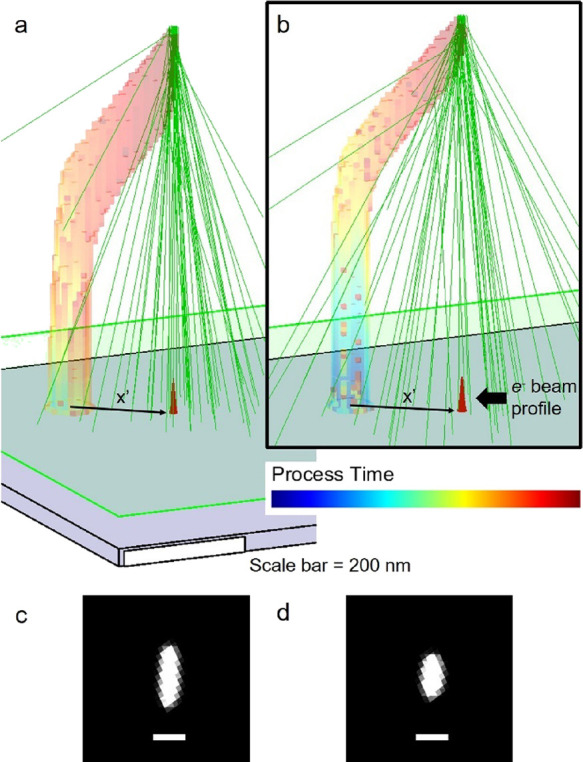
Calibration structure simulations at (a) ⟨E30:i35⟩ and (b) ⟨E10:i48⟩. The scale bar is shown superimposed on the side of the substrate as a white bar; scale bar, 200 nm. Fifty randomly selected PE trajectories (green line) are shown at the final beam impact position that led to deposition at the segment tip, so the reader may infer the convolution of the electron interaction volume (EIV) and the segment tip. Each rendering is partially transparent to reveal completely each PE trajectory through the deposit. The segment cross section oriented orthogonal to the segment axis is shown for both (c) ⟨E30:i35⟩ and (d) ⟨E10:i48⟩. The scale bars in panels (c) and (d) have a length of 50 nm.
In both renderings, a 3D image of the deposit geometry is presented where the segment element has reached a length of nominally S = 250 nm. The deposit consists of computation voxels with an edge length of 7 nm. A voxel is rendered as part of the deposit only when filled. The voxel hue represents the process time when filled. Voxels are rendered partially transparent to reveal the cumulative elastic scattering in the segment tip when the beam passes through many such voxels. Fifty randomly selected PE trajectories are shown as green traces, and their cumulative construct reveals the EIV distribution in the segment tip. SE trajectories are not shown.
The focal plane of the electron beam is shown at the partially transparent, green plane located 50 nm above the substrate surface, along with the beam trajectory (x′) in the plane for segment exposure. The electron beam probe current density profile is shown as the small Gaussian (red) distribution located on the focal plane. The height of the profile is arbitrary. The FWHM values of the probe are 6.5 nm @ 30 keV (Figure 3a) and 7.2 nm @ 10 keV (Figure 3b) as simulated. Beam impact with the segment occurs well above the focal plane position at the segment tip.
The most basic observation from Figure 3 is that PEs nearly always penetrate the segment element for both PE energies. On closer inspection, transmitted beam divergence is greater at 10 keV, even though the segment element is thinner at 10 keV. This observation reflects the increased probability of elastic scattering at lower beam energies as predicted by the Rutherford elastic scattering model.37 For this reason, a complex iSE″ distribution emerges at the tip, leading to a segment with a more circular cross section at Eo = 10 keV (Figure 3d), while a more elliptical cross section develops at 30 keV (Figure 3c) with the long axis of the ellipse oriented vertically.35 Please note that these cross sections were created by slicing orthogonal to the segment axis, not vertically.
The EIV renderings presented in Figure 3 serve two purposes. First, the iSE exposure area can be inferred from this diagram as approximately the region at the segment tip over which PEs both enter and exit the segment. This estimate is meaningful because the SE MFP is less than the voxel size and, thus, the extent of PE surface interactions controls the iSE spatial distribution. Later, the effective SE exposure area at the segment tip (ASE) will serve as a parameter to couple experimental exposure parameters to the DBEA model. For now, the reader is at least equipped with a mental picture of this area. Second, the EIV is an effective heat source due to the EEL taking place continuously, according to Bethe,37 along each PE trajectory. Specifically, the spatial concentration of the EIV to the segment tip supports favorably the later presented thermal model in DBEA where the segment tip is treated as a single “node” that receives heat “input” from the beam.
Segment Distortion Mechanism
Consider a nanoprinted segment after deflection/bending has evolved, as shown in Figure 4a. The simulated calibration structure has been sliced in the x′–z′ plane to reveal the deposit cross section. Clearly, the segment angle has steadily decreased along the s-coordinate, most notably starting at nominally 400 nm from the segment origin. Now, consider heat and precursor transport conditions at the conclusion of the pixel dwell time at the tip of the segment; in this snapshot of deposition, the beam is On and is about to be displaced to the next electron beam displacement. T(s) and C(s) are displayed at this moment in time in Figure 4b.
Figure 4.
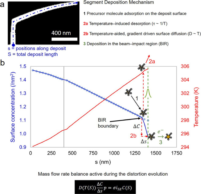
(a) Cross-sectional (x′, z′) slice through a simulated calibration structure exhibiting segment deflection/bending. The s-coordinate, with an origin on the substrate surface, is labeled on the diagram because gradients in temperature and precursor surface concentration directed along this dimension affect the development of segment deflection. (b) The steady increase in temperature in the BIR due to beam-induced heating steadily decreases the precursor surface concentration in this region. Ultimately, this reduces the deposition rate, causing the observed segment deflection. C(s) (blue line), Ceq(s) (blue circle), and T(s) (red line) during the final moments of continuous beam exposure at a pixel located at the segment tip. Ceq(s) (blue circle) has also been included for reference, and it was calculated using T(s) and the equation provided later in eq 5b. C(s) has reached the maximum surface concentration, predicted Ceq(s) at most points along the deposit, except in the BIR. At the BIR boundary, (1) the precursor adsorbed from the vapor phase either (2a) desorbs due to the elevated temperature or (2b) is swept into the BIR by surface diffusion. The latter mechanism sustains (3) continuous deposition of the segment via electron beam-stimulated precursor dissociation. This process is mathematically represented by the BIR precursor mass balance shown at the bottom of the figure.
For now, the reader is encouraged to take for granted the assumption of steady-state conditions during individual pixel exposures. Supporting data for this assumption is provided later in the paper.
Continuous segment deposition is controlled by the following sequence of events that represent the most probable pathways for deposition.
A reservoir of adsorbed precursor molecules, attached all along the segment surface, provides both local and stable sources of precursors to feed deposition in the BIR.
Precursor molecules transport to the BIR by a precursor surface concentration gradient established by beam dissociation by the Gaussian electron beam profile.
Electron-stimulated dissociation of the precursor leads to near steady-state deposition of the precursor, simultaneously maintaining the precursor surface concentration gradient that feeds growth during any given dwell period.
Data supporting this model of deposition is now presented.
The reservoir of precursor molecules coating the surface of the deposit is dominated by both the surface temperature and precursor adsorption rate. A stable temperature gradient is established along the deposit length as the rate of Joule heating in the BIR comes into balance with the extraction of heat from the pillar base into the substrate, with the substrate acting as a thermal sink. The resulting steady-state temperature distribution is shown in Figure 4b (red line). Previous simulation results27 have revealed that the temperature is nominally constant in the segment cross-sectional area for any given s-coordinate position. Thus, the relevant coordinate system is (s), in place of (x,y,z). A gradient in the equilibrium precursor concentration (outside the BIR) evolves in response to the temperature gradient, coupling to the heat flow through the temperature-dependent desorption term τ(T(s)):
| 4b |
where ko is the fundamental desorption attempt frequency, and Ea is the physical desorption activation energy. In fact, outside of the BIR, under nearly steady-state conditions, eq 3 is approximately described by
| 5a |
Figure 4b (blue circle) shows the equilibrium precursor surface concentration as a function of the s-coordinate based on the temperature along the s-coordinate, i.e., Ceq(s). Solving for the equilibrium precursor surface concentration gives
| 5b |
Ceq(s) is strongly correlated with the actual simulated precursor surface concentration along the deposit (blue line); notice that the Ceq(s) and C(s) curves are approximately equal outside the BIR. This correlation reveals that the precursor adhesion flux from the vapor phase is sufficient to maintain the equilibrium precursor surface concentration outside the BIR, even as the temperature increases. A rise in surface temperature increases the precursor desorption rate, thereby reducing the equilibrium precursor surface concentration at the BIR (eq 5b).
Precursor surface diffusion predominantly sustains the precursor flow to the BIR required for dissociation27 as indicated by the relatively steep gradient (dC/ds) observed at ∼s = 1300 nm (see Figure 4b, blue line). Thus, inside the BIR, vapor phase precursor replenishment alone cannot sustain the precursor dissociation rate. In fact, previously reported simulation results show that surface diffusion is the dominant precursor refresh mechanism to the BIR.27 These results indicate that a simple mass balance, applied at the BIR, describes segment deposition
| 6 |
where p is the perimeter of the segment cross section at the BIR, and iSE is the emitted secondary electron current in the BIR.
Past simulations revealed that the width of the precursor surface concentration gradient (Δs in Figure 4b) is constant during segment deposition.16 dC/ds is roughly linear in the BIR, which is also preserved over the course of segment deposition.16 Therefore, eq 6 may be simplified further to
| 7 |
where C(S) is the precursor surface concentration at the tip of the segment, and Ceq(S) is the equilibrium precursor surface concentration at the BIR edge (Supporting Information 10). This mass balance serves as a crucial mathematical component of the DBEA. Its utility as a substitution will become evident after presentation of the general deposition model that underpins the DBEA.
An Analytical Description of Segment Deposition
The DBEA creation begins with the definition of a simple growth rate model. The model is developed mathematically to include (1) the short-range (eq 7) and long-range (eq 5a) precursor transport effects that control nanoprinting physics, (2) calibration parameters critical to stable 3D nanoprinting, and (3) scanning parameters used during 3D nanoprinting. Finally, the solution is cast in the form of dwell time modulation per unit length in the focal plane, i.e., dt/dx′, for the easiest translation of solution results to exposure file creation.
Step 1: Deposition Rate Model
Analytical model development begins with a general deposition rate equation applicable to the total segment length. The segment elongates along the s-coordinate characterized by a total length of S at a given time. Local coordinates (x′, z′) conveniently confine segment deposition to a plane, orthogonal to the substrate surface (Figure 2b)
| 8 |
The vector magnitude provides a convenient way to combine known quantities toward a DBEA correction model.
| 9 |
The FEBID rate as a function of total length and time is given by
| 10 |
It will be shown below that steady-state deposition develops quickly during individual pixel exposures. The implications of this fact on the deposition rate (dS/dt) are 2-fold. First, the segment tip shape saturates after S ≅ 100 nm, which relaxes the iSE″ time dependence. Second, a constant surface temperature and a steady beam current combine to control C(S), imposing a nominally constant value during any single-pixel dwell. Thus, C(S) may be substituted for C(t) and the form of eq 10 is greatly simplified as
| 11 |
which is taken as constant during each individual pixel electron beam dwell time.
Step 2: Introduction of Scanning and Calibration Parameters
A mathematical model, if intended to correct a priori for deflection/bending, must (1) be constructed using scanning parameters that will be implemented during exposure and (2) expressed in terms of calibration parameters that guarantee 3D nanoprinting. In fact, the beam velocity already appears in the general growth rate equation (eq 8) as dx′/dt. The important calibration variable (ζ) can be imposed on the model by chain rule expansion applied to the vertical growth rate dz′/dt term
| 12 |
where dz′/dx′ = tan ζ, or
| 13 |
The strategy of DBEA is revealed in this mathematical format; C(S) is expected to decrease over the course of multiple pixel dwell times owing to the influence of the short- and long-range precursor gradients described previously. Thus, the left-hand side of eq 13 will decrease as a function of S. If it is desired to maintain segment linearity (tan ζ = constant), then a concomitant decrease in the right-hand side of eq 13 must occur. This is affected practically by beam deceleration, i.e., a decrease in dx′/dt. Importantly, eq 13 is enforced at each exposure pixel.
Step 3: Introduction of the Critical Mass Balance
The current DBEA form (eq 13) requires C(S), which must be simulated. Simulation execution is impractical when it is desired to have a rapid, on-demand CAD plug-in-based solution. Fortunately, the precursor transport balance (eq 7), defined at the BIR, makes it possible to substitute Ceq(S) in place of C(S). Solving for eq 7 for Ceq(T(S)) followed by substitution into eq 13 yields
 |
14 |
This substitution is powerful; a calculation of Ceq(S) requires only the temperature profile along the segment, which can be estimated using a simple thermal model, as opposed to numerically solving the heat equation (eq 4a). A thermal circuit network was developed for this purpose, and it is described below. Before summarizing the thermal circuit network (TCN), the final form of the DBEA is provided.
Step 4: Model Translation to Exposure
The DBEA ultimately provides a list of pixel dwell times as a function of x′ required to decelerate beam exposure toward maintaining a fixed segment angle. Commercially available pattern generators expect a list of coordinates and exposure times for proper pattern exposure. Thus, the DBEA solution must be expressed as dt/dx′, the change in exposure dwell time as a function of position in the focal plane, in preparation for mathematical integration for each pixel. Therefore, the general deposition rate equation can be rearranged algebraically to solve for the dwell time per pixel, or
| 15 |
In translation from eq 14 → eq 15, (1) iSE″ is deconstructed into the SE emission rate (iSE) and effective emission area (ASE), (2) the equilibrium precursor surface concentration eq 5b has been introduced, and (3) magnitude notation has been removed. Table 3 provides a list of all parameters that appear in the DBEA.
Table 3. Decelerating Beam Exposure Algorithm Parameters, Definitions, and Units.
| parameter | definition | units |
|---|---|---|
| Ω | molecular volume (deposit) | m3/molecule |
| σ | mean total electron impact dissociation cross section (precursor) | m2/e– |
| D | surface diffusion coefficient (precursor/deposit) | m2/s |
| Δs | span of precursor surface concentration gradient in the BIR | nm |
| δ | surface sticking probability (precursor/deposit) | (0 – 1) |
| τ | mean surface residence time (precursor/deposit) | ms |
| Φ | surface impingement flux (precursor) | molecule/m2 s |
| sp | monolayer precursor surface coverage (precursor/deposit) | molecule/m2 |
| T | temperature (deposit) | K |
| p | perimeter (deposit) super-ellipse model, exponent = 2.5 | nm |
| τo | thermal desorption (pre-exponential) | s |
| Ea, τ | thermal desorption (activation energy) | eV |
| Do | precursor surface diffusion (pre-exponential) | μm2/s |
| Ea, D | precursor surface diffusion (activation energy) | eV |
| iSE | emitted secondary electron current (electron/deposit) | e–/s |
| δI | SE emitted per PE @ steady segment growth | (0 – 1) |
| ASE | effective secondary electron emission area in the BIR | nm2 |
| Ceq | equilibrium precursor surface concentration | molecules/m2 |
| ζ | segment angle | degrees |
| τd | dwell time @ segment origin | ms |
| Λ | pixel point pitch | nm |
Steady-State Heat Transport during 3D Nanoprinting
Steady-state heat flow simplifies the mathematical treatment of heat transport for the 3D nanoprinting of mesh object models. This has the additional advantage of reducing computation time toward the goal of fast, i.e., <1 s, calculations. Again, an a priori correction as a CAD solution demands this speed. Fortunately, 3D nanoprinting exhibits two advantageous features related to quasi steady-state heat transport that ultimately reduce the calculation time below the specified limit.
Nondimensional analysis reveals that >99% of pixel dwell time is spent under steady-state heat transfer conditions. The Fourier number (Fo) defines the thermal penetration time (tFo) across a characteristic length scale (S) based on a set of materials parameters (k, cp, and ρ)
| 16 |
where Fo = 1/2 for the quasi 1D thermal transport expected in segments. This relatively brief thermal penetration time (10–6 s) is recovered for a characteristic length of S = 1 μm,27 which is a typical thermal path length through a representative calibration structure measured from the BIR to the substrate. Single-pixel exposure times for segment growth typically fall in the range of 10–2 to 10–3 s. So, only ∼0.01–0.1% of the pixel exposure time occurs under transient heat transport. Thus, it may be assumed that a constant temperature profile persists along the deposit during pixel exposure without incurring/accumulating a significant error. This statement is founded in the quality of DBEA results reported later, demonstrating bending correction.
A scheme of the thermal conditions over the course of single-pixel, segment exposure is shown in Figure 5a based on the Fo result. Importantly, this implies that the steady-state temperature distribution needs only be solved at a frequency of once per exposure pixel for any given mesh object model. However, imposing linear deposition (eq 15), coupled with steady-state conditions, makes it possible to reduce the frequency of thermal calculation to only once per segment, e.g., a reduction from ∼870 calculations to 1 calculation for an S = 1 μm segment inclined at ζ = 30°. Inspection of Fourier’s law supports additional simplification as now summarized.
Figure 5.
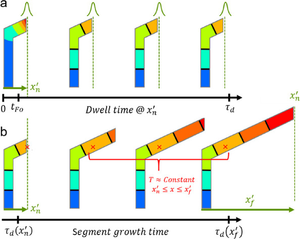
(a) Steady-state heat transfer approximates conditions during single-pixel dwell time. Schematic of the temperature profile in a calibration element over the course of a single-pixel dwell. The temperature increases in transitioning from blue to red. The steady-state assumption hinges on the fact that the spatial distribution of temperature is transient for only a brief period at the beginning of pixel exposure (t < tFo). (b) The thermal history during segment deposition may be extrapolated from a single, steady-state temperature distribution acquired during the beam irradiation at the tip of the final segment length. This assumption is only applicable in the limit of a linear segment, with a constant cross-sectional area along the segment length and a constant thermal conductivity.
The generalized Fourier’s law in heating rate (J/s) form must be conserved at points along the deposit under steady-state conditions.
| 17 |
Heating rate conservation may be achieved in multiple ways considering that k, dT/ds, and A⊥ may vary along the s-coordinate, thereby providing innumerable ways in which energy conservation may be satisfied. The generalized form is now revised for the case of linearized, 3D FEBID nanoprinting.
The internal nanostructure has been shown to vary negligibly over the segment length,6,38 simplifying k(s) to a constant thermal conductivity (k). The nanowire cross-sectional area is constant during linear segment deposition, so the cross-sectional area is also constant (A⊥).35 Thus, the conservation of qb required under steady-state conditions requires that dT/ds be constant. In fact, the 3D simulation results shown previously confirm this equality, showing a linear temperature profile during segment deposition (Figure 4b, red line) (Supporting Information 11). This means, assuming a constant deposited energy in the BIR, that the complete thermal history of the segment element can be computed by conducting a single heat transport calculation at the final exposure pixel.
The scheme of a recoverable thermal history is shown in Figure 5b. Various stages of segment deposition are shown, concluding with the steady-state temperature profile superimposed over the completed calibration structure under BIR irradiation at the final exposure pixel, i.e., the right-most calibration structure in Figure 5b. Consider the position (red cross mark) shown near the origin of the segment. The temperature at this location remains unchanged, moving back in history, all the way back to moment of formation of this position. Therefore, the temperature for all positions along the segment may be recovered from a single temperature profile derived from the completed segment!
A thermal circuit network (TCN) was devised to inform the temperature-dependent terms appearing in the DBEA, namely, D(T(S)) and τ(T(S)). TCN construction was inspired by the thermal transport simplifications just presented. Before describing the TCN, validation of a recoverable thermal history is provided using the numerical simulation of 3D nanoprinting.
Disclaimer on Presentation
Before the presentation of results, please note that 3D nanoprinting simulations, with and without DBEA correction, are presented in this section. Implicit in DBEA use is the application of the TCN. Thus, the justification of the steady-state principles applied in the TCN is provided through its performance prior to a complete description of the TCN. This was intentional; it is thought that digestion of the model is easier after reviewing preliminary results.
Simulation Validation of DBEA Thermal Calculations
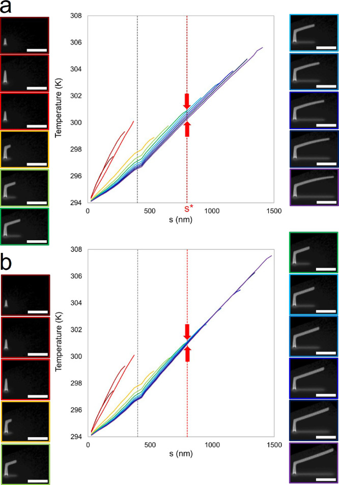
Simulations of the temperature profile at various stages of calibration structure deposition are shown in Figure 6a. The DBEA was not active during this nanoprinting simulation, resulting in undesirable segment deflection/bending. Subsequently, DBEA correction was applied to the calibration structure. Simulations of the temperature profile at various stages of deposition under DBEA are shown in Figure 6b. Each temperature profile presented is correlated with a simulated SEM image using a common color for the image border and T(s) trace.
Figure 6.
(a) Steady-state T(s) profiles acquired at various stages of uncorrected, calibration structure deposition. The results were derived from a single simulation of 3D nanoprinting ⟨E30:i35⟩. Simulated SEM images, acquired at 52° with respect to the substrate surface normal, are correlated with individual T(s) profiles using a unique image border color. The segment position s = s* serves as a reference position to compare uncorrected calibration structure deposition and (b) deposition using the DBEA.
Consider the population of thermal profiles after the completion of pillar deposition, i.e., s > 400 nm, as indicated by the gray vertical and dashed line (Figure 6a). Inspection of mature segment growth, i.e., those of substantial length indicated by blue/purple hues (s > s*), reveal individually a nearly constant slope dT/ds, which is independent of position along the segment. This data suggests that the assumption of a linear T(s) per segment is valid, even for uncorrected deposition. However, the same population of thermal profiles shows that at least for uncorrected nanoprinting, a single thermal estimate at segment completion (purple line, T(s)) does not provide a complete description of past thermal history.
Consider the position s* in Figure 6a. During deposition at s*, T ≅ 301 K in the BIR (dark green line, T(s)). However, the temperature steadily decreases at s* as deposition continues beyond this location, amounting to a decrease of >1 K, i.e., the span between the red arrows. The temperature decrease observed at the fixed position s* is ultimately caused by the steady decrease in segment cross-sectional area as deposition proceeds beyond this point (s > s*). The deposition rate at the tip steadily decreases for deposition beyond s* as C(s) decreases, which is of course temperature-dependent. Figure 7a demonstrates the evolution of C(s) for two specific calibration structures selected from Figure 6; notice that C(S) = 1.05/nm2 (TBIR ≅ 302 K) for the incomplete segment element (light blue line), which nominally decreases to C(S) = 1.00/nm2 (TBIR ≅ 305 K) at segment deposition completion (purple line). The steady decrease in the deposition rate is manifested structurally as a steady decrease in A⊥(s) (compare the segment tip thickness in the simulated SEM images with solid borders provided in Figure 7a, inset). This, in turn, progressively reduces the average PE path length through the BIR. EEL decreases, leading to a smaller effective Joule heating source term (qb).27 This cumulative process results in a progressive decrease in temperature at s* as qb steadily decreases at the tip with increased segment length.
Figure 7.
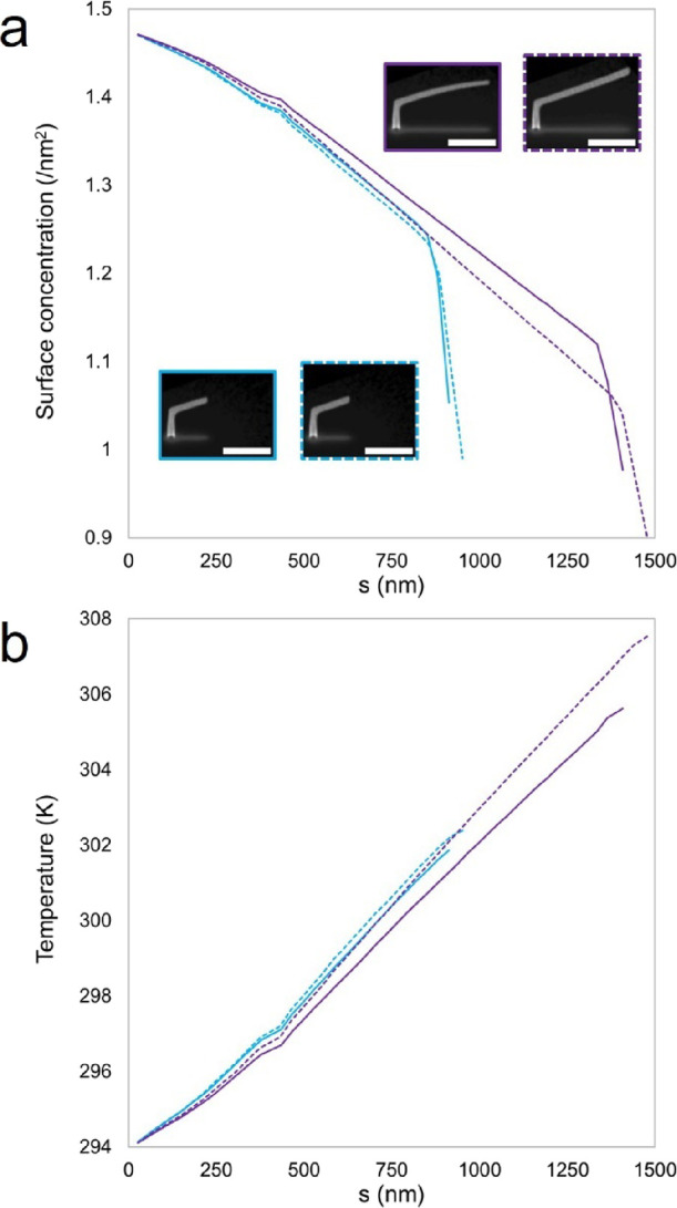
(a) Precursor surface concentration profiles C(s) acquired at the final moment of the single-pixel exposure for (1) two different stages (differentiated by color) of segment deposition and for (2) uncorrected and DBEA-corrected deposition using DBEA (solid lines vs hatched lines, respectively). Simulated SEM images, acquired at 52° with respect to the substrate surface normal, are correlated with individual C(s) profiles using a unique image border color and line type. (b) Complementary T(s) profiles to correlate the impacts of T(s) on C(s).
Applying the DBEA to our simulation prevents the segment deflection artifact (Figure 6b); inspection of simulated SEM images reveals the preservation of constant slope throughout simulated segment deposition. Complementary thermal profiles are presented under DBEA correction (Figure 6b) to directly compare the DBEA effect with profiles derived from uncorrected deposition (Figure 6a). Notably, the DBEA correction collapses the temperature variation at first observed at s* under uncorrected deposition (compare Figures 6a and 6b @ red arrows). So, dT/ds and T(s) are both approximately conserved as deposition progresses under DBEA. This observation correlates with the maintenance of a constant (A⊥) throughout segment deposition using DBEA. Thus, the thermal history is recoverable from the final thermal profile using the DBEA! Importantly, this fact applies over the segment length range (s = 800–1500 nm) most prone to deflection. Notice that dT/ds and T(s) are both conserved as deposition progresses under DBEA in this segment length range. Thermal history recovery seems a valid feature to include in the TCN based on these supporting 3D nanoprinting simulations.
Finally, note that the thermal history is not recoverable at the earliest stages of segment deposition using the final T(s), i.e., compare the lack of temperature profile overlap at the yellow/green line (T(s)) and purple line (T(s)) in Figure 6b. In other words, these T(s) profiles do not overlap in the range of s ≅ 400–700 nm. How then does DBEA preserve the segment angle? Fortuitously, by measuring the initial segment angle at Δs = 250 nm from the segment origin during calibration, the variability exhibited in this region is included in the calibration process.
Thermal Circuit Network
The thermal circuit network (TCN) will now be explained using a representative mesh object model as an example. The example network highlights important TCN features including the nodal heating rate (J/s) balance underpinning the model, the partial network concept, and the algorithm rules and details making the TCN applicable to any general mesh object model.
The purpose of the TCN is to solve for the temperature at each node present in the network. The mesh object model in any geometric state other than the final model will be referred to as a partial network. Any node in contact with the substrate is assigned a constant temperature; the DBEA treats the substrate as a bulk, thermal sink. Once node temperatures are computed, the temperature at any position along a given nanowire can be reconstructed, assuming a linear temperature gradient.
A TCN must be reconstructed and solved as each additional segment is added to the mesh object model. This reconstruction frequency is based on the steady-state heat transport assumptions validated in the previous section. Ultimately, the total number of TCN reconstructions required for a complete description of thermal conditions throughout deposition equals the total number of segments in the mesh object model. Table 4 provides a list of parameters used in the TCN.
Table 4. Thermal Circuit Network Parameters.
| parameter | definition |
|---|---|
| G | thermal conductance |
| S | final nanowire/segment length |
| fα | fraction applied to absorption path through deposit (fitting parameter) |
| fU | fraction of EEL contributing to Joule heating |
| tζ | segment thickness |
| wζ | segment width |
| A⊥ | segment cross-sectional area |
| α | primary electron path length through nanowire/segment |
| i | index over nanowires providing heat inflow by thermal conduction |
| I | number of nanowires providing heat inflow by thermal conduction into the current node |
| o | index over nanowires providing heat outflow by thermal conduction |
| O | number of nanowires providing heat outflow by thermal conduction into the current node |
A heat transfer rate balance is solved at each node in the partial network, excluding those in contact with the substrate, according to
| 18 |
where G is the nanowire thermal conductance, and I/O are the total number of segments (adding/subtracting) thermal energy flow to/from the node by heat conduction. Nanowire conductance
| 19 |
depends on the thermal conductivity and the segment cross-sectional area. Please note that the segment cross-sectional area depends on the segment angle A⊥(ζ) and this dependence is derived from calibration experiments (Supporting Information 2).
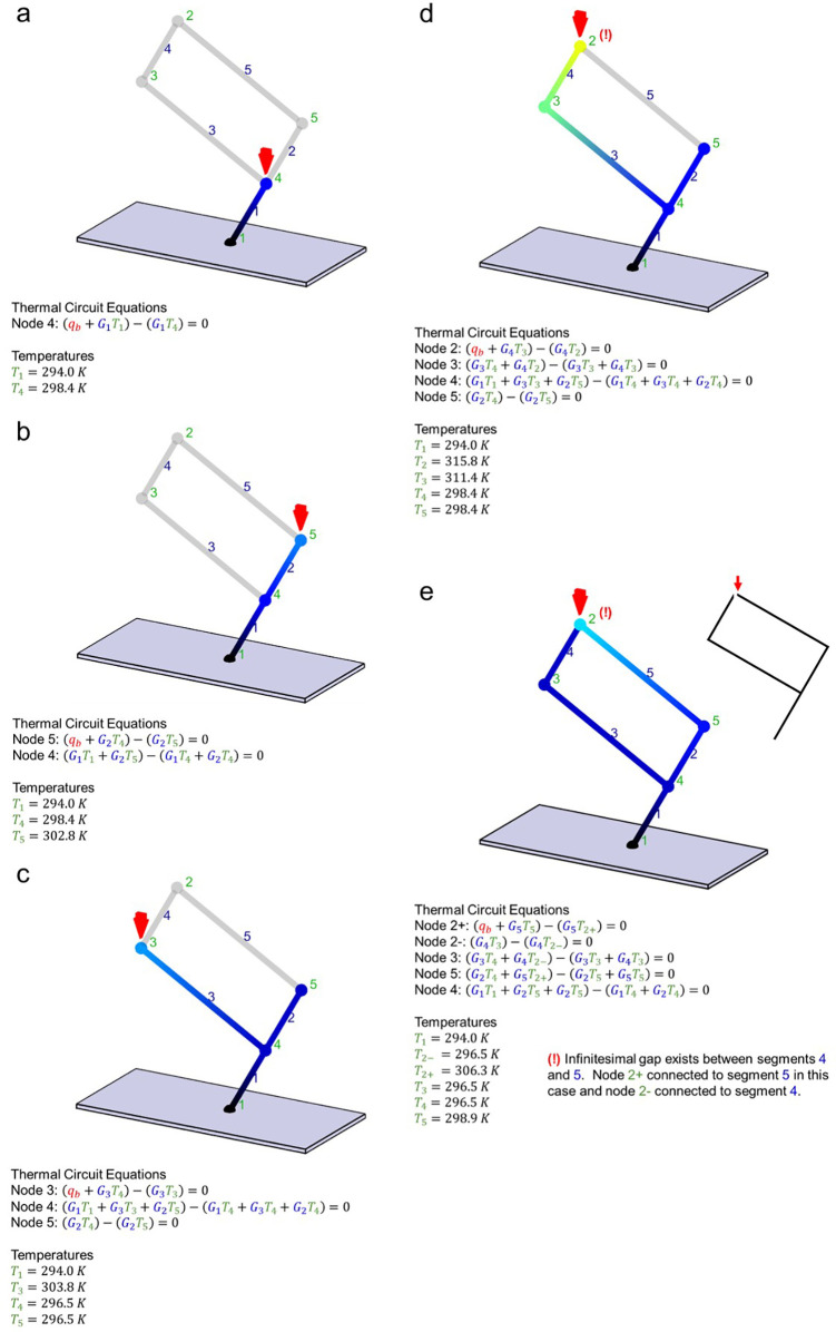
Figure 8a–e shows the order of segment nanoprinting for an example closed-frame mesh object model containing six nanowires. The time order of nanoprinting takes place from (a) to (e). In the first example, a single energy rate balance equation is constructed. Please note that the actual segment thickness and width, as they vary with (ζ), are not portrayed in the CAD model rendering in favor of a simple rod of circular cross section for simplicity.
Figure 8.
Closed-frame mesh object model example showing the thermal circuit network required at each stage of deposition for ⟨E30:i35⟩. These “partial” networks are shown in (a) → (e). Nodes are indicated with green integers and nanowires/segments with blue integers. The node irradiated by the electron beam is shown using a red arrow. Color shading shows temperature variations along nanowires, while actual temperatures are provided for each node based on the conditions reported in Supporting Information 1. Partially transparent nanowires in the partial network indicate nanowires that have yet to be deposited.
Closed-frame nanoprinting begins with the deposition of a segment (Figure 8a). A single energy rate balance equation is required to solve for the temperature at the nanowire terminal node 4●, since 1● is in contact with the substrate. The electron beam impact (red arrow) at node 4● leads to a heating rate balance between a source of thermal power (qb) and a heat conduction outflow to the substrate through 1-. Notice that the energy rate balance provided in Figure 8a has been parsed into bracketed terms representing heat inflows and outflows, i.e., a reconfiguration of eq 18. Next, important aspects regarding TCN behavior and construction are summarized.
Heat flow follows the least resistive path to the substrate heat sink (Figure 8c). In the case of partial networks containing isolated and branching elements, the temperature of the entire branch will reach thermal equilibrium. This can be seen in Figure 8c in the single branch segment 2- where the temperatures of nodes 4● and 5● are equal. Heat cumulatively flows from the irradiated node 3●, via 3- → 1-, to the substrate thermal sink in this partial network. This is the nature of steady-state heat transport.
Converging nanowires, such as the merging of segments 4- and 5- (Figure 8e), require special treatment when constructing the TCN. Specifically, an infinitesimal gap must be included in the mesh network at node 2● to correctly reconstruct the thermal history during the deposition of segment 5- considering that segments 4- and 5- are only in contact at the final moments of segment 5- deposition. As a result, in the final model shown, the network path 4- → 3- is an isolated branch with an equilibrium temperature at all nodes included in the branch, e.g., 2●, 3●, and 4●. In principle, 2● has been separated into two nodes in this case (Supporting Information 12).
Thermal Circuit Network Source Term
BIR heating occurs as primary electrons experience inelastic scattering inside the deposit. The fraction of inelastic electron energy loss that leads to heating was determined previously (fU = 0.86).27 The remainder of electron energy lost generates secondary electrons. A fraction of these SEs are both emitted and induce deposition. The total inelastic electron energy loss per unit length (dE/dz′) is estimated in the TCN using the modified Bethe expression.37 Integration to calculate the total energy loss rate per primary electron is limited to a maximum length along the primary electron beam trajectory (α) determined by the segment angle and segment thickness (tζ) as summarized in Figure 9. The heat source term used in the TCN, applied at the BIR, is
| 20 |
where qe is the charge per electron, and fα is the fraction of the segment thickness the PE actual passes through in transit through the segment tip.
Figure 9.
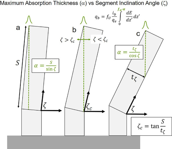
Energy absorption in the segment element by inelastic electron energy loss depends strongly on the deposit thickness along the electron beam path (α) because primary electron trajectories transmit through the deposit during deposition. The thermal circuit network (TCN) model uses a simple rectangular model to determine the path length through the deposit based on the segment thickness (tζ) and segment angle (ζ). (a) The absorption thickness (α) depends on the total segment length (S), at least beyond (b) the critical segment angle (ζc). Below the critical segment angle, (c) the absorption thickness depends on tζ and ζ. Deviations of real primary electron trajectories due to elastic scattering in the deposit are captured in the DBEA model using a calibration factor (fα) that is multiplied by the absorption thickness. The Joule heating rate (qb) is calculated in the TCN model using the equation shown. Most terms are defined in Table 4. The inelastic electron energy loss per unit length along the electron beam path (dE/dz′) is estimated using the modified Bethe expression.37
Importantly, fα serves as a calibration factor in DBEA. Specifically, the calibration factor is varied to determine the best value that leads to linear deposition correction. The correction factor for DBEA is applied as a multiple of the segment absorption thickness for two reasons.
First, a steadily increasing temperature is the dominant factor leading to segment bending. Thus, fα should be applied within the mathematical model directly to a temperature-dependent term. The absorption thickness through the deposit controls the heating rate, thereby directly inducing the bending mechanism. In summary, α·fα should be viewed as an effective absorption thickness.
Second, the magnitude of fα affording calibration can be compared with the expected deviation of electron trajectories (Figure 3) from the idealized linear model (Figure 9) to gauge the realistic merit of the value. For example, at relatively large electron primary beam energies, i.e., Eo = 30 keV, elastic scattering is minimized and a value of fα ∼ 1 is expected. Conversely, non-negligible elastic scattering is expected at lower primary electron beam energies, i.e., Eo = 10 keV. In this regime, fα < 1 is anticipated.
DBEA Calibration
Calibration of the decelerating beam exposure algorithm, or DBEA, is now summarized. DBEA usage here applies only to the correction of the calibration structure. Extrapolation of the DBEA calibration to more complex mesh object models is described and tested later. The summary example presented in Figure 10 applies to the primary deposition parameters of ⟨E30:i35⟩.
Figure 10.
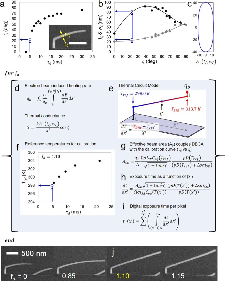
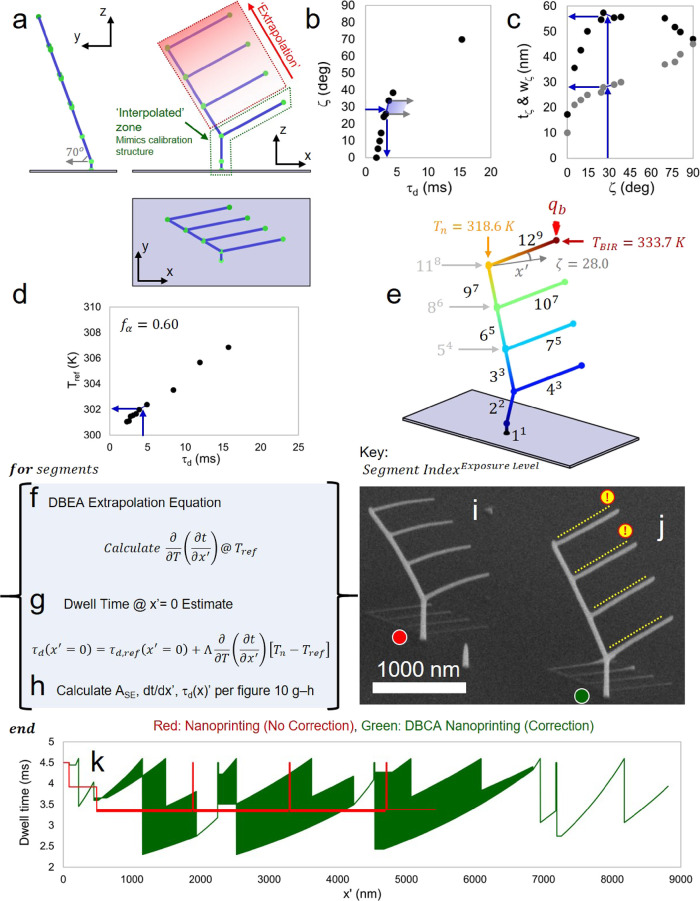
Visual summary of DBEA calibration using ⟨E30:i35⟩. (a) The calibration curve required for uncorrected deposition is again required for DBEA in addition to (b) complementary measurements of the thickness (tζ) and width (wζ), also made at s = 250 nm. (c) A super-ellipse best models the segment cross-sectional area A⊥(tζ,wζ) with an exponent of n = 2.5.35 The super-ellipse cross section shown was calculated for ζ = 22°, i.e., the blue, open circle data points in panels (a) and (b). (d) The electron beam heating rate (qb) and the thermal conductance of the segment depend on tζ, wζ, and ζ and are requisite parameters for the thermal circuit network, or TCN. (e) The TCN calculation yields two important parameters required for the DBEA; it directly computes the reference temperature at the segment origin (Tref) and indirectly computes the linear temperature gradient along the segment using TBIR, Tref, and the segment projected total length (X′). (f) Reference temperature as a function of pixel dwell time for six calibration structures with various segment angles. The calibration factor (fα = 1.10) was used, and it is the value that yields linear segments. (g) The effective secondary electron exposure area at the BIR (ASE) serves as a convergence parameter linking the DBEA expression (eq 15) with the pixel dwell time determined from experimental calibration. (h) Once fα has been determined, the change in exposure time per unit length (dt/dx′) may be computed for all x′. (i) Integration across each pixel yields the digital dwell time per pixel τd(x′). (j) Example experimental structures grown with various fα terms.
Additional calibration structure measurements are required to calibrate the DBEA because the segment cross-sectional area variation with ζ must be known; the segment width (wζ) and segment thickness (tζ) must be measured (Figure 10a), along with ζ. The nature of the variation of tζ and wz (Figure 10b) with the segment angle, as well as beam energy and current, has been shown by Gazzadi et al.15 for different precursors, and the involved growth effects were recently elaborated in detail.35 Please note that the cross-sectional shape of the nanowires can strongly vary for different precursors15 and for different microscope settings.35
Importantly, the measurements are taken at the standard position of s = 250 nm. This value is a convenient choice with regards to ζ; it is small enough such that the segment has yet to exhibit significant deflection while long enough to make a statistically significant estimate of ζ. Regarding the former advantage, the initial phase of deposition (s < 250 nm) is approximated as unaffected by thermal effects. Implementation of this concept will become apparent below.
A typical model segment cross-sectional area is provided in Figure 10c for ζ = 22°. The cross-sectional area as shown is orthogonal to the s-coordinate A⊥(tζ,wz), and it was derived from the open circle data points (blue) in Figure 10a,b. Previous experiments35 have revealed a super-ellipse cross-sectional area as a representative of this segment feature, with an exponent of 2.5.
The remaining steps for DBEA calibration must be carried out for a range of fα values to converge on the proper value that yields linear segment deposition. In the present work, multiple calibration structures spanning the full range of segment angles ζ = 0–90° were deposited for each value of fα to gauge the merit of a single constant value of fα for correction; too small a value (e.g., fα < 1.10) leads to a downward bending, relative to the electron beam trajectory, while too large a value leads to an upward deflection (e.g., fα > 1.10).
DBEA calibration continues with application of the TCN to the calibration structure. Importantly, the TCN is applied to the calibration structure CAD linear model, in other words, not the distorted result from real deposition. The reason is that the DBEA is imposing a linear correction using the initial linear segment inclination, so the TCN must be linear to obtain a realistic estimate of the temperature distribution in the calibration structure. The TCN requires calculating the heating rate at the BIR (qb) and the thermal conductance (G) of the segment (Figure 10d). These terms depend on tζ and wζ explaining the addition of these parameters to the calibration procedure for DBEA. The critical TCN output for DBEA calibration is the temperature at the origin of the segment, the so-called reference temperature (Tref), and the linear temperature gradient along the segment projection (Figure 10e). The latter is derived from the BIR temperature (TBIR) and the length of the segment. Reference temperatures are shown in Figure 10f for six calibration structures as a function of the pixel dwell time (these results were generated using fα = 1.10, which is the correct DBEA calibration for the ⟨E30:i35⟩ experiments reported).
The DBEA must be quantitatively coupled to the TCN results to ensure that the DBEA equation reproduces the experimental electron beam dwell time per pixel when segment deposition begins, i.e.,
| 21 |
This is achieved by rearranging eq 15 and solving for ASE, which is the effective emission area of secondary electrons leading to deposition (Figure 10g). Simulation results show that this parameter varies with segment angle because the EIV convolution with the segment tip shape varies with ζ. So, it is thus an ideal situation to allow this last unknown parameter to be effectively “calibrated away”; in this way, a description of the segment tip shape as a function of segment angle, such as shown in Figure 1i, is avoided!
| 22 |
Crucially, notice that dt/dx′ has been replaced with τd/Λ in eq 22, enforcing the calibration procedure on DBEA, and that ζ equals the initial linear estimate also derived from calibration. Temperature-dependent parameters appearing in eq 22 are determined from the reference temperature at the segment origin.
DBEA correction is applied (Figure 10h) using the variation in temperature predicted by
| 23 |
Primary electron beam exposure is digital in real experiments. This requires translating the analog DBEA model (Figure 10h) into a digital representation over the range x′ = 0:X′. On a per pixel basis, the electron beam dwell time per pixel is
| 24 |
where the summation extends over the number of pixels along x′, which is X′/Λ. DBEA calibration executed at ⟨E30:i35⟩ resulted in a calibration solution at fα = 1.10 (Figure 10j).
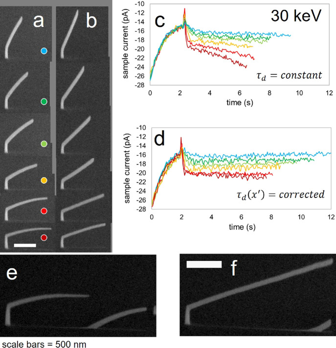
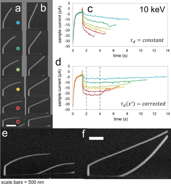
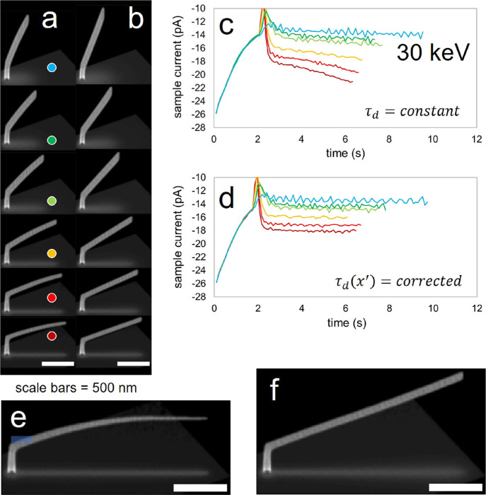
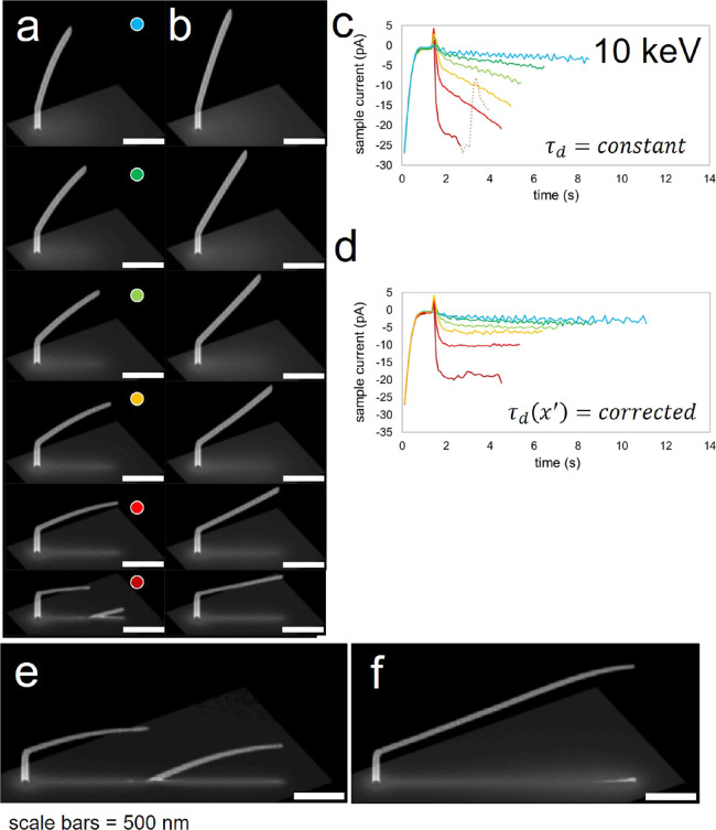
A single calibration factor (fα = 0.95) yielded segment deflection correction for a variety of calibration structures with different segment angles (Figure 11) at ⟨E30:i35⟩. Successful correction is qualitatively evaluated from SEM images based simply on the straightness/linearity of a DBEA-corrected segment. SEM images acquired before DBEA application (Figure 11a, column of images) and after DBEA application (Figure 11b, column of images) reveal the successful correction based on visual inspection.
Figure 11.
(a) Calibration structures (×6) of variable segment angle deposited at ⟨E30:i35⟩. (b) DBEA correction of the calibration structures shown in panel (a) using fα = 0.95. (c) Sample current profiles acquired during deposition for each calibration structure shown in panel (a). (d) Sample current profiles acquired during DBEA-corrected growth revealing the constant sample current associated with the deposition of linear segments. In both panels (c) and (d), the segment deposition begins at the time associated with the relatively sharp peak of maximum current at >2 s. (e) A relatively long segment, with a low initial segment angle (ζ = 22°) exhibits severe negative deflection, ultimately fragmenting due to a loss of e– beam–segment contact. As a result, a new segment emerges on the substrate surface as the beam continues to scan in the segment direction in the focal plane. (f) DBEA correction not only prevents the fragmentation but also produces the desired linear segment. Experimental conditions reported in Supporting Information 1.
Fortunately, a quantitative measure for straightness/linearity also exists, which does not require electron imaging but rather monitoring of electrical current during deposition.27Figure 11c shows sample current traces collected during deposition with a time resolution of 58 ms. The current collection geometry mimics a Σi = 0 circuit node where electrons captured by the deposit/substrate/stage are detected using a picoamperemeter. Emitted BSE, FSE, and SE contribute a current loss term relative to the node, while PE absorption provides a positive contribution. The details of current collection and current profile analysis have been carefully described elsewhere.27 Here, it is enough to point out that a constant current during segment deposition indicates a linear segment.
For example, notice the steady trend toward a more negative current for the smallest uncorrected segment angle (Figure 11c, dark red line, trace). The signature of the beginning of segment deposition is the maximum current spike when depositing a calibration structure, i.e., when a segment is deposited beginning from the tip of a pillar. This spike appears beyond 2 s in Figure 11c. Notice that the steady change in current (beyond ∼2 s) correlates with the deflection of the segment (Figure 11a, ●). The deflection is a consequence of the steady temperature increase at the tip (as the segment elongates) and reflects a decrease in the deposition rate in the BIR. The rate decrease manifests physically as a decrease in segment cross-sectional area. This, in turn, reduces the effective area (ASE) from which SEs may be emitted. Thus, fewer SE electrons are generated (which otherwise contribute to a positive stage current), which accounts for the tendency toward a more negative stage current with segment elongation. DBEA prevents this decrease in deposition rate by increasing the pixel dwell time as a function of x′. Therefore, a properly corrected deposition should yield a constant sample current signal over the course of segment deposition. The DBEA-corrected sample traces in Figure 11d display nearly constant sample current traces for the DBEA segments (Figure 11b).
The results presented in Figure 11 validate the DBEA as a correction scheme for several reasons. First, uncorrected segments with ζ → 0° are the most prone to deflection, yet they can be the most difficult to correct because the calibration curve is the steepest in this region, i.e., max(dζ/dτd) (see Figure 10a). Relatively small changes in τd impart significant changes in ζ. For this reason, DBEA performance at low segment angles (Figure 11e,f) is encouraging where deflection correction extends to ∼3 μm, well beyond the initial segment length on which the correction procedure is based, i.e., 250 nm. As shown in Figure 11f, the correction works well out to 3 μm, where at this length a second segment emerges from the substrate due to the longer dwell times. Next, a further observation that validates DBEA is the fact that a single calibration value (fα = 0.95) corrects for a multitude of segment angles. This suggests that the mathematical model is valid; otherwise, e.g., if multiple fα values were required, perhaps any model could be made to fit the results. Last, the value of fα = 0.95 is nominally 1. Thus, because the calibration factor is imposed as a multiplier to the experimental measured absorption thickness, convergence of fα × α to the absorption thickness (α) seems to validate the TCN model component of DBEA where, at Eo = 30 keV, fα = 1 is expected due to low elastic scattering (Figure 3a). Further evidence in favor of DBEA is the extension of applicability to a lower primary electron beam energy (Figure 12).
Figure 12.
(a) Calibration structures (×6) of variable segment angle deposited at ⟨E10:i48⟩. (b) DBEA correction of the calibration structures shown in panel (a) using fα = 0.53. (c) Sample current profiles acquired during deposition for each calibration structure shown in panel (a). (d) Sample current profiles acquired during DBEA reveal the constant sample current associated with the deposition of linear segments. In both panels (c) and (d), the segment deposition begins at the time associated with the relatively sharp peak of maximum current at >1.5 s. (e) A relatively long segment with a low initial segment angle exhibits severe negative deflection, ultimately fragmenting due to a loss of e– beam–segment contact. As a result, a new segment emerges on the substrate surface as the beam continues to scan in the segment direction in the focal plane. (f) DBEA correction ensures linearity up to the point that the segment merges with a second-order artifact, which is grown by the transmitted primary electron beam. Experimental conditions reported in Supporting Information 1.
The DBEA was also tested favorably at ⟨E10:i48⟩, yielding again a constant calibration factor (fα = 0.53) (Figure 12a–d) as well as reasonable performance in the long segment limit (Figure 12e,f). As a measure of reproducibility, the long segment deposition was conducted using a recalibration of deposition and initialization of the FEI Nova microscope where the experiments were performed. The calibration factor changed to fα = 0.65 for DBEA correction. Therefore, the difference in these values represents the variation associated with realigning the GIS, manually focusing the beam, etc. Such a difference was also found for experiments conducted using Eo = 30 keV where, in March 2020, fα = 0.95 compared with fα = 1.10, which was required for duplicate experiments in August 2020.
The segment thickness model (Figure 9) used as part of the TCN may also influence the relationship between fα and the primary electron beam energy (Eo). Specifically, the reduction in fα observed at ⟨E10:i48⟩ (fα = 0.53), relative to ⟨E30:i35⟩ (fα = 0.95), can be explained by the deposition simulations displayed in Figure 3 in conjunction with the absorption thickness model implemented in the DBEA (Figure 9). Consider the scheme provided in Figure 13, which shows how the α calculation may deviate from the true value of α at the tip and at relatively lower Eo.
Figure 13.
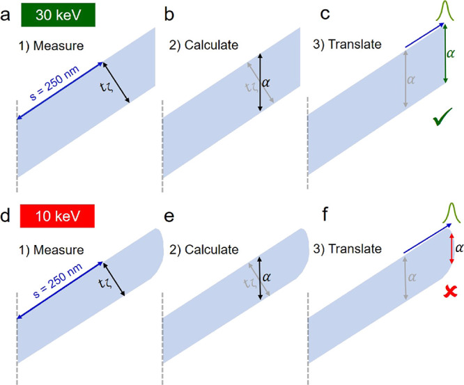
Scheme of the absorption thickness (α) calculation, for use at the segment tip as applied in the thermal circuit network (TCN) model, based on measurements of the segment thickness elsewhere, i.e., at s = 250 nm. The error incurred by this method increases as the electron beam energy decreases, e.g., (a–c) at Eo = 30 keV, the method is appropriate, while (d–f) at Eo = 10 keV, a rounded segment tip leads to a higher error in α. Nonetheless, the correction factor (fα) calibrates out any such error.
To begin, tζ is measured at any position along the segment where the steady-state thickness has developed (Figure 13a). The TCN model calculates α based on a calibration measurement of tζ (Figure 13b and equation in Figure 9). Finally, α is translated to the segment tip as a representative of this dimension (Figure 13c).
This technique is appropriate at Eo = 30 keV where the segment has a nearly vertical terminal (xe′) face at the tip (see simulation in Figure 3a). Also, the segment tip shape has been recently characterized experimentally (see Figure 7 in ref (35)). However, at Eo = 10 keV (Figure 13d–f), the real value of α is less than the calculated α because the tip is curved. The segment tip is curved at Eo = 10 keV (Figure 3b). This could explain the reduced value of fα = 0.53 at Eo = 10 keV relative to fα = 1, which would be expected for a vertical segment tip terminus. As a reminder, elastic scattering influences are not considered in this ideal analysis of the real segment tip shape influence.
The DBEA calibration section concludes with the presentation of complementary simulations that mimic the experiments carried out at ⟨E30:i35⟩ (Figure 14) and ⟨E10:i48⟩ (Figure 15). The simulation reproduces many experimental features, particularly deposit geometry and sample current profiles, yet the focus here is to point out one specific difference; the temperature as predicted by simulations is on the order of ∼10 K higher than the temperature predicted by the TCN (discussed later). This mismatch will be revisited later in Discussion.
Figure 14.
Simulations of calibration structure deposition at ⟨E30:i35⟩, which directly complement the experiments shown in Figure 11. (a) Calibration structures of variable segment angle. (b) DBEA correction of the calibration structures shown in panel (a) using fα = 0.65. Sample current profiles are provided for simulations of (c) uncorrected deposition and (d) DBEA-corrected simulations. Simulations of DBEA correction were also successful in the long segment limit when comparing (e) uncorrected and (f) DBEA-corrected calibration structures. Simulations conditions are reported in Supporting Information 1 along with characterization results.
Figure 15.
Simulations of calibration structure deposition at ⟨E10:i48⟩, which directly complement the experiments shown in Figure 12. (a) Calibration structures of variable segment angle. (b) DBEA correction of the calibration structures shown in panel (a) using fα = 0.40 (dark red), fα = 0.60 (red), fα = 0.7 (orange, green, and cyan), and fα = 0.90 (blue). This was the only situation where multiple values of the correction factor were required at a constant electron beam energy and current setting. Sample current profiles are provided for simulations of (c) uncorrected deposition and (d) DBEA-corrected simulations. Simulations of the DBEA correction were reasonably successful in the long segment limit when comparing (e) uncorrected and (f) DBEA-corrected calibration structures, although relative to experiments, DBEA simulations did exhibit some deflection at a segment length of S ≅ 3 μm. Simulations conditions are reported in Supporting Information 1 along with characterization results.
Figure 16 shows the typical dwell time variation required, as a function of scan length, to correct various segment angles, in this case, for the condition ⟨E10:i37⟩. The pillar element height supporting the segment was 480 nm. The origin of the scanning projection (x′) is the segment origin (x′ = 0). A few additional features of DBEA are revealed via inspection of Figure 16.
Figure 16.
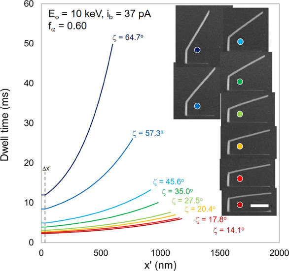
DBEA-generated exposure coordinates of the electron beam dwell time (τd) as a function of electron beam scan position in the focal plane (x′) for calibration structures deposited at ⟨E10:i37⟩. Notably, a single calibration factor of fα = 0.60 corrected the library of calibration structures shown. Scale bars, 500 nm. Simulations conditions are reported in Supporting Information 1 along with characterization results.
DBEA must not influence the original segment angle, as measured from the uncorrected segment deposition. The reason is that ζ is measured at s = 250 nm during the derivation of the calibration curve. Later, this same value is used to calculate ASE, which effectively couples experimental characterization and the DBEA model. ζ modification is avoided using a constant dwell time (τd) over a finite initial beam scanning length (Δx′) equal to nominally half the pillar width (32 nm). This delay in activating DBEA preserves the initial segment angle observed for uncorrected deposition, at least within the measurement error of ζ, which is Δζ = ±2°.
Last, the degree of DBEA compensation required clearly increases as a function of segment angle. Mathematically, the rate of change of the exposure dose per unit length (d2t/dx′2) increases with ζ. This phenomenon is caused by an increase in the absorbed energy per PE due to the increase in α as a function of ζ.4
DBEA Implementation
High-fidelity replication of complex mesh object models using the DBEA nanoprinting strategy is a strong validation of the model merit. Toward this end, the mesh object model shown in Figure 17 was printed. While the previous success of the model verifies the worthiness of DBEA application in an “interpolated” regime (see previous section), the devised mesh object model in Figure 17a tests the model in a more “extrapolated” mode.
Figure 17.
(a) A 3D Comb mesh object model was created to test DBEA beyond the simple interpolation required for DBEA calibration. The extrapolation scheme is demonstrated here using the topmost segment as an example exposure element. (b–d) The segment angle (b) is used to interpolate the following values from the available calibration data including the initial electron beam dwell time, segment thickness (c), segment width (c), and reference temperature (d). (e) Thermal circuit network (TCN) estimates for the segment origin and terminus temperatures. The order of exposure is described in Supporting Information 13 using the superimposed notation of (segment index)exposure level. (f, g) The initial dwell time is estimated based on the difference between the reference temperature, determined from a calibration structure of the same angle, and the TCN-calculated temperature. (h) τd(x′) may then be calculated based on the DBEA calibration algorithm provided in Figure 10g,h. SEM images of (i) uncorrected 3D comb deposition and (j) DBEA-corrected deposition reveal the enhancement in replication afforded by the DBEA method. Finally, (k) a plot of the DBEA electron beam dwell time (ms) versus the exposure number (green line) reveals (1) a relatively longer total deposition time, compared to uncorrected deposition (red line), and (2) wide green bands, which represent simultaneous segment deposition on exposure levels 3, 6, and 9; the plot is actually oscillating between the exposure of two different segments (ζ = 28° and ζ = 54.5°), which is these apparent band regions. Simulations conditions are reported in Supporting Information 1 along with characterization results.
Interpolation and extrapolation, in the context used here, refer to the difference between the segment origin reference temperature calculated during calibration and the origin temperature of any given segment constituting the mesh object model. By using a reference temperature, DBEA application should extend beyond the calibration structure geometry, to a general mesh object model, because a thermal analysis relaxes the geometric dependence. This hypothesis was tested using a “3D Comb” mesh object model (Figure 17a). As described next, certain design elements of the 3D Comb were expected to be favorable for revealing the replication error. First, however, the DBEA implementation steps will be described using the 3D Comb as an example.
The 3D Comb is shown in the traditional side–top–side CAD perspective format in Figure 17a. The following DBEA steps are executed for each segment in the mesh object model.
DBEA begins with a calculation of the first segment angle using the (x, y, z) coordinates of the initial and final vertices. Calibration information is then gathered. First, the initial dwell time is interpolated from the calibration curve based on the segment angle (Figure 17b). Interpolation is indicated in Figure 17b as a linear segment (blue line) spanning the two experimental data points enclosing the calculated angle. Next, the segment thickness (tζ) and width (wζ) (Figure 17c) are interpolated from calibration data. Finally, the reference temperature (Tref) is interpolated using the initial dwell time (Figure 17d).
TCN application follows the gathering of calibration parameters (Figure 17e). As an example, the topmost segment in the 3D Comb has been chosen as the demonstration segment to show the key data collected from the TCN results: the initial node temperature (Tn) and the BIR temperature (TBIR) when the electron beam exposes the final vertex as indicated by qb (→ red). Up to this point, the DBEA implementation algorithm has followed exactly the DBEA calibration. Now, the algorithms diverge with DBEA implementation requiring extrapolation beyond the original calibration to enable DBEA correction for the more complex 3D Comb.
Extrapolation is required because the initial segment node temperature (Tn = 318.6 K) deviates significantly from the interpolated value of Tref ≅ 302 K based on the calibration structure of equal angle (ζ = 28°). A significant decrease in thermal conductance has resulted due to a longer path length to the ground from the segment origin causing the elevation in Tn, relative to Tref.
The extrapolation procedure requires first calculating the derivative in temperature of dt/dx′
| 25 |
where ASE is calculated as presented before in Figure 10h. Importantly, both ASE and ∂2t/∂T∂x′ are calculated at Tref. Extrapolation is then applied via a linear order variation in the dwell time variable to generate an estimate of the initial exposure dwell time
| 26 |
where the initial dwell time per segment angle is indicated now as τd,0.
Equipped with τd,0(Tn), steps in Figure 10f–h are repeated, but in this iteration, Tn is used to solve for the final τd(x′), instead of Tref. As a reminder, τd(x′) is the primary electron beam dwell time variation per unit beam scan length required to correctly deposit a linear segment. The merits of the 3D Comb as a test deposit are now described prior to a presentation of deposition results.
The 3D Comb replicates the calibration structure geometry in the vertical dimension, which effectively exposes each additional segment added to more extreme thermal conditions. In other words, the nature of vertical construction by additive deposition leads to an increase in the initial segment temperature in the z-coordinate. Of course, this is caused by the increasing thermal path length to the ground and the concomitant decrease in thermal conductance. Further, deflection is easily measured after deposition based simply on the spacing variation between deposited segments on adjacent exposure levels. Last, the 3D Comb design is rotated to lie in a plane inclined at 20° off vertical to ensure that the electron beam only exposes the BIR over the duration of 3D Comb deposition; the transmitted beam does not intersect lower exposure levels containing deposition. Multiple beam intersections cannot be currently handled by the TCN but is certainly capable of being modified to do so.
DBEA results for the 3D Comb are now presented. Figure 17i shows the experimental uncorrected printing of the 3D Comb. Clearly, the magnitude of segment negative deflection worsens for each additional segment deposited as seen by the decrease in the initial segment angle for each additional segment added to the 3D Comb, relative to the CAD (Figure 17e).
Careful inspection of the substrate surface below the uncorrected 3D Comb deposit reveals a 2D Comb “shadow” projection. This artifact is caused by ancillary deposition driven by the transmitted electron beam, which occurs in tandem with the intended 3D Comb deposition.
DBEA correction greatly improves the fidelity of the 3D Comb (Figure 17j). SEM imaging reveals that nearly parallel segments are deposited, at least when compared with a superimposed grid (yellow dashed line). The grid lines have a common inclination angle, making it possible to compare ζ among the four segments in the comb. A defect, or error, becomes visible in the third segment deposited in the form of a divergence between the superimposed grid line and the segment. Interestingly, the nature of the defect is an incorrect segment angle, rather than the re-emergence of a gradual deflection. This suggests that the defect emerges due to a compounding of small structural errors over time, rather than a failure in DBEA. The origin of this accumulating defect could arise from many sources including a minor error in reported/simulated FEBID parameters (Table 2) or drifting microscopy conditions. Nonetheless, DBEA-assisted nanoprinting yields a marked improvement over uncorrected printing.
3D Comb printing used the maximum intermittent exposure mode.17 Successful DBEA application in this mode provides further indirect support of the validity of the steady-state heat transport assumption. In Supporting Information 13, this exposure mode is described first before making the connection between this mode of deposition, deposition outcomes, and steady-state heat transfer. In summary, Supporting Information 13 reveals that the fraction of total segment deposition time spent in transient heat transfer conditions is slightly greater when (1) multiple segments are exposed simultaneously and/or (2) the pixel dwell time exceeds a hardware imposed maximum of 4.6 ms. Factor (1) introduces a beam sweeping motion, while factor (2) forces multiple exposures per pixel to accumulate the pixel dwell time needed. It is expected that the electron beam is perturbed in a position somehow during this latter situation, although exactly how is not known. Nevertheless, the quality of DBEA correction shown in Figure 17j (and later in Figures 18 and 19) indicates that the steady-state assumption is still a valid one; otherwise, DBEA would not work!
Figure 18.
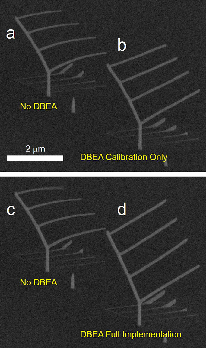
The utility of the DBEA extrapolation approach was quantified by carrying out a deposition (1) using DBEA calibration while (2) not enforcing DBEA extrapolation. First, the 3D Comb design was deposited (a) without correction as well as (b) using DBEA calibration only. In the latter case, Tref values are used to calculate dt/dx′ for each segment. Next, (c) uncorrected deposition was again conducted as a reference, along with (d) full DBEA implementation. During full DBEA implementation, the difference between Tref and the actual segment origin temperature also factors into the calculation of τd(x′) via d2t/dx′dT. Thus, the DBEA extrapolation quality may be gauged by comparing the replication quality between the 3D comb deposits shown in panels (b) and (d). Simulations conditions are reported in Supporting Information 1 along with characterization results.
Figure 19.
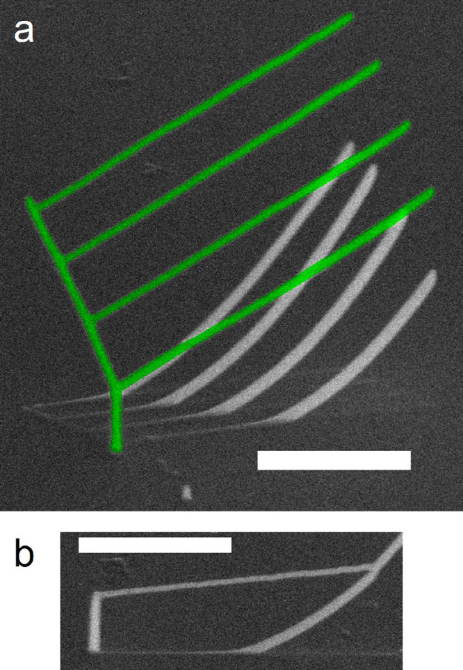
(a) DBEA implementation enhanced high-fidelity CAD replication, even for a segment element length of S = 2400 nm, when the 3D Comb design was modified to further test the extrapolation method. (b) In fact, DBEA implementation works well under the challenging conditions of ζ → 0° to such a degree that straightness/linearity is preserved up to the limit where the segment merges with its ancillary complementary deposit caused by the transmitted primary electron beam. Simulations conditions are reported in Supporting Information 1 along with characterization results.
Briefly, segment exposure occurs on exposure levels 3, 6, and 9 (see Figure 17e) where the electron beam sweeps back and forth between the segments on a per beam exposure basis. These periods are revealed in the plot of electron beam dwell time per exposure (Figure 17k) as the wide green bands. Although unresolved, the plot is rapidly oscillating between the two different exposure times. Nonetheless, the complex structure of the electron beam dwell time per pixel can be appreciated in the diagram. Also, by superimposing the uncorrected dwell time exposure pattern (red line), it is clear that the DBEA correction requires a longer total exposure time. For the case of the 3D Comb, the total process time for the uncorrected Comb was t = 18.5 s, while the DBEA correction required t = 31.6 s, nearly twice as long.
The quality of the DBEA extrapolation technique may be resolved by depositing the 3D Comb with DBEA calibration but not DBEA implementation (Figure 18). Also, this example acts to further stress the DBEA method increasing extrapolation by increasing the 3D Comb segment length by 50% from 800 to 1200 nm. Uncorrected 3D Comb nanoprinting is shown in Figure 18a for reference, followed by nanoprinting using only DBEA calibration (Figure 18b). Specifically, this means that the reference temperature is interpolated using Tref vs τd (Figure 10f), but τd,0 is not extrapolated to account for the actual segment origin temperature calculated by the TCN, i.e., eq 26 is not used. The results are poor relative to the previous demonstration of 3D Comb printing with DBEA extrapolation (Figure 17j). Nonetheless, the results are better than uncorrected deposition. More importantly, this set of experiments quantifies the range of applicability of interpolated DBEA based on calibration structures. Uncorrected 3D Comb deposition was again executed (Figure 18c) followed by full DBEA implementation (Figure 18d). DBEA implementation produced far better results than when using DBEA calibration alone, producing an encouraging fidelity of 3D Comb CAD.
DBEA replication continued to produce high-fidelity replication when again doubling the 3D Comb segment length to 2400 nm (Figure 19). The nature of the ancillary deposition observed in this case is worth explaining in more detail.
Under the 3D Comb exposure conditions, the ancillary deposition at the substrate becomes substantial because the dwell time per pixel increases exponentially with segment length under DBEA implementation, e.g., see again Figure 16. For this reason, the second-order, emerging ancillary substrate segments grow to such an extent that they grow and merge with the CAD-defined segments. The deposition rate of the surface-bound segments is larger than the rate exhibited by the 3D Comb segment elements because the former are grown directly from the surface, which resides at a relatively lower temperature because of the reduced path length to the substrate. Lower temperatures yield a large equilibrium surface coverage of the precursor and, therefore, a larger deposition rate and larger angle. As the dwell time increases for longer segments, the ancillary deposition angle increases and eventually merges with the lower angle segment. Fortunately, as shown in Figure 19b, DBEA implementation works well under the challenging conditions of ζ → 0° to such a degree that straightness/linearity is preserved up to the limit where the segment merges with its ancillary complementary deposit initiated by the transmitted primary electron beam.
Discussion
To overview the validity of the simulation-informed DBEA analytical solution, we list the following algorithm attributes. Certain facts will also be provided with additional supporting evidence. We conclude with a final fact that also serves as an ideal summary of the design, motivation behind, and performance of DBEA.
-
1)
A single value of fα corrects for segment bending across a range of segment angles. If fα varied for each segment angle, one could perhaps argue that any mathematical model could be made to work. Incidentally, DBEA was found to work better for experiments than simulations. Although a single value of fα was required for ⟨E30:i35⟩, multiple values were required at ⟨E10:i48⟩. The reason for this is currently unclear and will be explored in future work.
-
2)
The model was found to result in high-fidelity CAD replication at two different primary electron beam energies. In particular, the reduction from Eo = 30 keV → 10 keV leads to non-negligible elastic scattering, which challenges the assumption that α is equal to the PE beam trajectory through the segment.
-
3)
The merit of the model is also encouraging when considering that the value of fα × α is on the order of the real absorption thickness. In other words, if fα were an order of magnitude smaller or larger, then its application as a multiplication factor with the absorption thickness (α) would be nonphysical.
The astute reader may have identified the contradiction present in fact 2. This contradiction may be posed as a question. How can the DBEA solution be effective at low beam energy when the solution itself does not account for the changing physics? The answer to this question lies in mathematical application of the calibration factor. The calibration factor effectively reduces the path length over which energy is lost, thus reducing the beam heating rate. However, by application as a multiplication factor with the geometric absorption thickness, i.e., as fα × α, the term is more influential as α increases. This is one reason that DBEA seems to work at low beam energy. The 3BID simulation can be used to clarify this point.
The geometric absorption thickness (α) is plotted against the true path length traveled by primary electrons in the segment tip, considering the elastic scattering of transmitted electrons (SPE) (Figure 20). α was measured from simulated SEM images of simulation results using the method presented in Figure 13. SPE is the average path length through the segment tip during irradiation where the average was taken over all electrons in the simulated dose. Please note that SPE is tortuous because of elastic scattering. Simulation data is provided at both Eo = 10 keV (red circles) and Eo = 30 keV (blue squares). The gray dashed line represents the limit of no elastic scattering where the geometric absorption thickness equals the actual electron path through the segment tip.
Now, consider the Eo = 30 keV data set. Elastic scattering effects are a minimum as α tends to zero, which is seen as a clustering of low-angle data points (■23.6°, ■30.0°, ■38.6°) on the correlation line. As α increases, the SPE through the deposit deviates from α, decreasing in magnitude. Elastic scattering is driving PEs out of the deposit, off the maximum center line depth. The blue fit line captures this trend. Fortuitously, fα × α counteracts this effect by reducing the absorption thickness by a larger amount for relatively thicker deposits. The light blue data points (■) show the results of fα × α vs SPE at Eo = 30 keV: DBEA is driving the relationship toward SPE ≅ fα × α, which is expected at Eo = 30 keV where elastic scattering is minimized. In fact, the DBEA model predicts SPE < fα × α for all segment angles. This is expected! As the scheme shows in Figure 20b, the finite size of the electron beam, relative to the segment thickness, causes a significant number of PEs to transmit through thinner portions of the segment thickness, thereby reducing the effective geometric absorption thickness explored by the average PE to a value less than α. Results at Eo = 10 keV (●) further support the conclusions reached regarding the physical interpretation of fα.
Elastic scattering is more pronounced at Eo = 10 keV. For this reason, α vs SPE deviates from the correlation line at smaller segment angles relative to the results shown for Eo = 30 keV. Further, the magnitude of the deviation is greater at constant ζ, at Eo = 10 keV, relative to Eo = 30 keV. DBEA replication predicts a real absorption thickness fα × α < SPE, which is the correct trend for the same reasons explained for the Eo = 30 keV case.
Finally, it should be noted that the result at 10 keV and ζ = 77.2° is not ideal. Inspection of the deposit replication by virtual SEM (Figure 15b) shows that some negative deflection is still observed. The reason for the deviation in this relatively high segment angle simulation is currently unclear.
The simulation analysis above also sheds light on the difference between the experimentally determined parameters of fα = 0.95 at Eo = 30 keV and fα = 0.65 at Eo = 10 keV. Elastic scattering deviates transmitted PEs more severely at Eo = 10 keV, which reduces the absorption thickness needed in the DBEA model to correct for deflection and replicate CAD. Last, one could ask: Why do simulations require a different fα relative to experiments? The answer in this case is simple: the 1D thermal simulation, which produces the nearly instantaneous predictions of temperature required for a priori implementation, predicts a different BIR temperature when compared with the 3D thermal treatment present in the nanoprinting simulation. Specifically, the full 3D simulation accounts for the spreading out of the Joule heating source term over the EIV–deposit convolution. Figure 21 shows that the difference in dimensionality leads to, in general, a lower predicted temperature by ∼10 K for simulations, relative to 1D TCN simulations. Fortunately, fα can absorb this error for DBEA replication.
-
4)
The method can be extended beyond basic DBEA calibration conditions to more complex mesh object models. The basic premise used to construct the model, toward this demonstration, is summarized in Conclusions.
Figure 20.
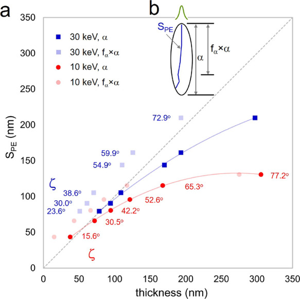
(a) Mean primary electron path length through the deposit during BIR irradiation including elastic scattering (SPE) versus the thickness of the segment (see Figures 9 and 13). SPE is derived from the Monte Carlo algorithm executed as part of the 3D nanoprinting simulation, while α is calculated using tζ measurements from the virtual SEM images of simulation results. The appropriate interpretation of the thickness axis is α for darker data points and fα × α for the lighter data points. Simulations executed at Eo = 30 keV are represented with square data points, while those at Eo = 10 keV are represented using circular data points. In the absence of elastic scattering, SPE = thickness as shown by the gray dashed correlation line. The simulation conditions are provided in Supporting Information 1. (b) Schematic segment slice (ellipse). The primary electron beam trajectory lies in the plane of the slice. The purpose of the schematic is to show the relationship between SPE, α, and fα × α. The data was derived from the simulations shown in Figure 14b (30 keV) and Figure 15b (10 keV).
Figure 21.
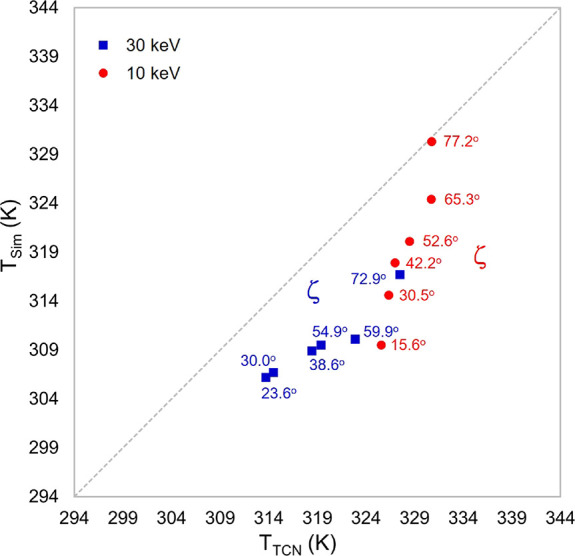
Thermal circuit network (TCN) model temperature prediction versus the temperature estimated by the 3D nanoprinting simulation. The simulation temperature represents the maximum temperature on the BIR surface during the final pixel exposure on the segment element of a calibration structure (see Figures 14b and 15b). Simulations at Eo = 30 keV (solid blue square) and Eo = 10 keV (solid red circle) are presented.
Conclusions
Surface temperature gradients imposed by beam heating during deposition ultimately controls the ability to replicate CAD models during the 3D FEBID nanoprinting of mesh object models. For this reason, reference temperatures are estimated and stored, as a function of segment angle, during DBEA calibration as these temperatures are the most influential variable affecting replication. For mesh object models that deviate from the simple calibration geometry, the difference between the reference temperature and the complementary temperature in the complex model is ultimately used to engineer replication. In this way, the most influential factor affecting deposition is used to engineer the replication solution.
Modulation of the electron dose during deposition was chosen to counteract heat evolution because changes in the dose do not affect thermal conditions, at least under conditions of steady-state heat transfer. Thermal conditions during FEBID are determined by a rate balance (J/s), i.e., a steady state persists during deposition where the beam heating rate in the BIR is balanced with deposition cooling rate at points of deposit–substrate contact. Thus, the electron beam current effects thermal conditions, while the electron beam dose does not. This explains why the electron beam current must be specified for each DBEA calibration, e.g., unique calibrations were required at ⟨E10:i48⟩ and ⟨E10:i37⟩.
Precursor surface concentration gradients ultimately act as the link that translates the surface temperature gradient into unwanted geometric artifacts; quasi steady-state precursor/mass flow conditions persist where the precursor surface desorption rate increases with surface temperature, thereby decreasing the deposition rate in the BIR because of a lower surface concentration of the precursor. The precursor-limited regime (PLR) controls the deposition rate, even at the earliest stages of deposition before the thermal gradients have developed along the deposit. Nonetheless, this PLR-compromised deposition rate is aided by precursor surface diffusion due to a natural gradient that develops due to electron-stimulated precursor dissociation at the BIR. The spatial extent of this gradient is limited mostly to the electron beam size due to the variation in current density over the electron beam profile. All these physical/chemical factors are included in the DBEA model in the form of a steady mass/precursor flow rate balance at the BIR boundary, steady over the course of any given pixel exposure period. The high quality of DBEA replication in the extrapolation mode seems to support the proposed mathematical, physical chemistry-based DBEA model as proposed.
Acknowledgments
J.D.F. and P.D.R. acknowledge that research was conducted at the Center for Nanophase Materials Sciences, which is a DOE Office of Science User Facility. The financial support by the Austrian Federal Ministry for Digital and Economic Affairs and the National Foundation for Research, Technology and Development is gratefully acknowledged (Christian Doppler Laboratory DEFINE, Austria).
Supporting Information Available
The Supporting Information is available free of charge at https://pubs.acs.org/doi/10.1021/acsomega.2c06596.
Details on simulation parameters for Figures 3, 4, 6, 7, 13, and 14 and details on experimental parameters for Figures 10–12 and 15–18 details on segment angle calibration; statement on precursor coverage; explanations on reference frames; beam focus considerations; definition of SEI; statement on calibration procedure; considerations on nanoparticle metal–carbon matrix composite composition; justification for simulations; definition of equilibrium precursor surface concentration; explanation for temperature deviations from linearity; note about the gap in TCN calculation; details on intermittent segment exposure (PDF)
The authors declare no competing financial interest.
Supplementary Material
References
- Hirt L.; Reiser A.; Spolenak R.; Zambelli T. Additive Manufacturing of Metal Structures at the Micrometer Scale. Adv. Mater. 2017, 29, 1–30. 10.1002/adma.201604211. [DOI] [PubMed] [Google Scholar]
- Utke I.; Moshkalev S.; Russell P. E.. Nanofabrication Using Focused Ion and Electron Beams: Principles and Applications ;1st ed.; Utke I.; Moshkalev S.; Russell P. E., Eds.; Oxford University Press: New York, 2012. [Google Scholar]
- Winkler R.; Fowlkes J. D.; Rack P. D.; Plank H. 3D Nanoprinting via Focused Electron Beams. J. Appl. Phys. 2019, 125, 210901. 10.1063/1.5092372. [DOI] [Google Scholar]
- Fowlkes J. D.; Winkler R.; Lewis B. B.; Stanford M. G.; Plank H.; Rack P. D. Simulation-Guided 3D Nanomanufacturing via Focused Electron Beam Induced Deposition. ACS Nano 2016, 10, 6163–6172. 10.1021/acsnano.6b02108. [DOI] [PubMed] [Google Scholar]
- Lewis B. B.; Mound B. A.; Srijanto B.; Fowlkes J. D.; Pharr G. M.; Rack P. D. Growth and Nanomechanical Characterization of Nanoscale 3D Architectures Grown via Focused Electron Beam Induced Deposition. Nanoscale 2017, 9, 16349–16356. 10.1039/C7NR05274J. [DOI] [PubMed] [Google Scholar]
- Winkler R.; Schmidt F.-P.; Haselmann U.; Fowlkes J. D.; Lewis B. B.; Kothleitner G.; Rack P. D.; Plank H. Direct-Write 3D Nanoprinting of Plasmonic Structures. ACS Appl. Mater. Interfaces 2017, 9, 8233–8240. 10.1021/acsami.6b13062. [DOI] [PubMed] [Google Scholar]
- Keller L.; Huth M. Pattern Generation for Direct-Write Three-Dimensional Nanoscale Structures via Focused Electron Beam Induced Deposition. Beilstein J. Nanotechnol. 2018, 9, 2581–2598. 10.3762/bjnano.9.240. [DOI] [PMC free article] [PubMed] [Google Scholar]
- Winkler R.; Lewis B. B.; Fowlkes J. D.; Rack P. D.; Plank H. High-Fidelity 3D-Nanoprinting via Focused Electron Beams: Growth Fundamentals. ACS Appl. Nano Mater. 2018, 1, 1014–1027. 10.1021/acsanm.8b00158. [DOI] [Google Scholar]
- Sattelkow J.; Fröch J. E.; Winkler R.; Hummel S.; Schwalb C.; Plank H. Three-Dimensional Nanothermistors for Thermal Probing. ACS Appl. Mater. Interfaces 2019, 11, 22655–22667. 10.1021/acsami.9b04497. [DOI] [PubMed] [Google Scholar]
- Vavassori P.; Pancaldi M.; Perez-Roldan M. J.; Chuvilin A.; Berger A. Remote Magnetomechanical Nanoactuation. Small 2016, 12, 1013–1023. 10.1002/smll.201503351. [DOI] [PubMed] [Google Scholar]
- Mulders J. J. L. Practical Precursor Aspects for Electron Beam Induced Deposition. NANO 2014, 1, 74–79. 10.2478/nanofab-2014-0007. [DOI] [Google Scholar]
- Barth S.; Huth M.; Jungwirth F. Precursors for Direct-Write Nanofabrication with Electrons. J. Mater. Chem. C 2020, 8, 15884–15919. 10.1039/D0TC03689G. [DOI] [Google Scholar]
- Liu Z. Q.; Mitsuishi K.; Furuya K. Features of Self-Supporting Tungsten Nanowire Deposited with High-Energy Electrons. J. Appl. Phys. 2004, 96, 619–623. 10.1063/1.1755434. [DOI] [Google Scholar]
- Liu Z. Q.; Mitsuishi K.; Furuya K. Three-Dimensional Nanofabrication by Electron-Beam-Induced Deposition Using 200-KeV Electrons in Scanning Transmission Electron Microscope. Appl. Phys. A: Mater. Sci. Process. 2005, 80, 1437–1441. 10.1007/s00339-004-2999-x. [DOI] [Google Scholar]
- Gazzadi G. C.; Frabboni S.; Menozzi C. Suspended Nanostructures Grown by Electron Beam-Induced Deposition of Pt and TEOS Precursors. Nanotechnology 2007, 18, 445709 10.1088/0957-4484/18/44/445709. [DOI] [Google Scholar]
- Fowlkes J. D.; Winkler R.; Mutunga E.; Rack P. D.; Plank H. Simulation Informed CAD for 3D Nanoprinting. Micromachines 2020, 11, 8. 10.3390/mi11010008. [DOI] [PMC free article] [PubMed] [Google Scholar]
- Fowlkes J. D.; Winkler R.; Lewis B. B.; Fernández-Pacheco A.; Skoric L.; Sanz-Hernández D.; Stanford M. G.; Mutunga E.; Rack P. D.; Plank H. High-Fidelity 3D-Nanoprinting via Focused Electron Beams: Computer-Aided Design (3BID). ACS Appl. Nano Mater. 2018, 1, 1028–1041. 10.1021/acsanm.7b00342. [DOI] [Google Scholar]
- Skoric L.; Sanz-Hernández D.; Meng F.; Donnelly C.; Merino-Aceituno S.; Fernández-Pacheco A. Layer-by-Layer Growth of Complex-Shaped Three-Dimensional Nanostructures with Focused Electron Beams. Nano Lett. 2020, 20, 184–191. 10.1021/acs.nanolett.9b03565. [DOI] [PubMed] [Google Scholar]
- Weitzer A.; Huth M.; Kothleitner G.; Plank H. Expanding FEBID-Based 3D-Nanoprinting toward Closed High-Fidelity Nanoarchitectures. ACS Appl. Electron. Mater. 2022, 4, 744–754. 10.1021/acsaelm.1c01133. [DOI] [Google Scholar]
- Plank H.; Winkler R.; Schwalb C. H.; Hütner J.; Fowlkes J. D.; Rack P. D.; Utke I.; Huth M. Focused Electron Beam-Based 3D Nanoprinting for Scanning Probe Microscopy: A Review. Micromachines 2020, 11, 48. 10.3390/mi11010048. [DOI] [PMC free article] [PubMed] [Google Scholar]
- Keller L.; Al Mamoori M. K. I.; Pieper J.; Gspan C.; Stockem I.; Schröder C.; Barth S.; Winkler R.; Plank H.; Pohlit M.; et al. Direct-Write of Free-Form Building Blocks for Artificial Magnetic 3D Lattices. Sci. Rep. 2018, 8, 6160. 10.1038/s41598-018-24431-x. [DOI] [PMC free article] [PubMed] [Google Scholar]
- Fernández-Pacheco A.; Skoric L.; De Teresa J. M.; Pablo-Navarro J.; Huth M.; Dobrovolskiy O. V. Writing 3D Nanomagnets Using Focused Electron Beams. Materials 2020, 13, 3774. 10.3390/ma13173774. [DOI] [PMC free article] [PubMed] [Google Scholar]
- Sanz-Hernández D.; Hierro-Rodriguez A.; Donnelly C.; Pablo-Navarro J.; Sorrentino A.; Pereiro E.; Magén C.; McVitie S.; de Teresa J. M.; Ferrer S.; et al. Artificial Double-Helix for Geometrical Control of Magnetic Chirality. ACS Nano 2020, 14, 8084–8092. 10.1021/acsnano.0c00720. [DOI] [PMC free article] [PubMed] [Google Scholar]
- Skoric L.; Donnelly C.; Hierro-Rodriguez A.; Cascales Sandoval M. A.; Ruiz-Gómez S.; Foerster M.; Niño M. A.; Belkhou R.; Abert C.; Suess D.; et al. Domain Wall Automotion in Three-Dimensional Magnetic Helical Interconnectors. ACS Nano 2022, 16, 8860–8868. 10.1021/acsnano.1c10345. [DOI] [PMC free article] [PubMed] [Google Scholar]
- Höflich K.; Jurczyk J. M.; Madajska K.; Götz M.; Berger L.; Guerra-Nuñez C.; Haverkamp C.; Szymanska I.; Utke I. Towards the Third Dimension in Direct Electron Beam Writing of Silver. Beilstein J. Nanotechnol. 2018, 9, 842–849. 10.3762/bjnano.9.78. [DOI] [PMC free article] [PubMed] [Google Scholar]
- Pakeltis G.; Hu Z.; Nixon A. G.; Mutunga E.; Anyanwu C. P.; West C. A.; Idrobo J. C.; Plank H.; Masiello D. J.; Fowlkes J. D.; et al. Focused Electron Beam Induced Deposition Synthesis of 3D Photonic and Magnetic Nanoresonators. ACS Appl. Nano Mater. 2019, 2, 8075–8082. 10.1021/acsanm.9b02182. [DOI] [Google Scholar]
- Mutunga E.; Winkler R.; Sattelkow J.; Rack P. D.; Plank H.; Fowlkes J. D. Impact of Electron-Beam Heating during 3D Nanoprinting. ACS Nano 2019, 13, 5198–5213. 10.1021/acsnano.8b09341. [DOI] [PubMed] [Google Scholar]
- De Teresa J.; Orús P.; Córdoba R.; Philipp P. Comparison between Focused Electron/Ion Beam-Induced Deposition at Room Temperature and under Cryogenic Conditions. Micromachines 2019, 10, 799. 10.3390/mi10120799. [DOI] [PMC free article] [PubMed] [Google Scholar]
- Hinum-Wagner J.; Kuhness D.; Kothleitner G.; Winkler R.; Plank H. FEBID 3D-Nanoprinting at Low Substrate Temperatures: Pushing the Speed While Keeping the Quality. Nanomaterials 2021, 11, 1527. 10.3390/nano11061527. [DOI] [PMC free article] [PubMed] [Google Scholar]
- Friedli V.; Utke I. Optimized Molecule Supply from Nozzle-Based Gas Injection Systems for Focused Electron- and Ion-Beam Induced Deposition and Etching: Simulation and Experiment. J. Phys. D: Appl. Phys. 2009, 42, 125305 10.1088/0022-3727/42/12/125305. [DOI] [Google Scholar]
- Thorman R. M.; Kumar T. P.; Fairbrother D. H.; Ingólfsson O. The Role of Low-Energy Electrons in Focused Electron Beam Induced Deposition: Four Case Studies of Representative Precursors. Beilstein J. Nanotechnol. 2015, 6, 1904–1926. 10.3762/bjnano.6.194. [DOI] [PMC free article] [PubMed] [Google Scholar]
- Hagen C. W. The Future of Focused Electron Beam-Induced Processing. Appl. Phys. A: Mater. Sci. Process. 2014, 117, 1599–1605. 10.1007/s00339-014-8847-8. [DOI] [Google Scholar]
- De Teresa J. M.; Córdoba R.; Fernández-Pacheco A.; Montero O.; Strichovanec P.; Ibarra M. R. Origin of the Difference in the Resistivity of As-Grown Focused-Ion- and Focused-Electron-Beam-Induced Pt Nanodeposits. J. Nanomater. 2009, 2009, 1–11. 10.1155/2009/936863. [DOI] [Google Scholar]
- Randolph S. J.; Fowlkes J. D.; Rack P. D. Effects of Heat Generation during Electron-Beam-Induced Deposition of Nanostructures. J. Appl. Phys. 2005, 97, 124312. 10.1063/1.1942627. [DOI] [Google Scholar]
- Winkler R.; Fowlkes J. D.; Rack P. D.; Kothleitner G.; Plank H. Shape Evolution and Growth Mechanisms of 3D-Printed Nanowires. Addit. Manuf. 2021, 46, 102076 10.1016/j.addma.2021.102076. [DOI] [Google Scholar]
- Perentes A.; Bachmann A.; Leutenegger M.; Utke I.; Sandu C.; Hoffmann P. Focused Electron Beam Induced Deposition of a Periodic Transparent Nano-Optic Pattern. Microelectron. Eng. 2004, 73, 412–416. [Google Scholar]
- Joy D. C. An Introduction to Monte Carlo Simulations. Scanning Microsc. 1991, 5, 329–337. [Google Scholar]
- Frabboni S.; Gazzadi G. C.; Felisari L.; Spessot A. Fabrication by Electron Beam Induced Deposition and Transmission Electron Microscopic Characterization of Sub-10-Nm Freestanding Pt Nanowires. Appl. Phys. Lett. 2006, 88, 213113–213116. 10.1063/1.2206996. [DOI] [Google Scholar]
Associated Data
This section collects any data citations, data availability statements, or supplementary materials included in this article.


