Abstract
Two-dimensional materials are trending nowadays because of their atomic thickness, layer-dependent properties, and their fascinating application in the semiconducting industry. In this work, we have synthesized MoSe2 and WSe2 nanosheets (NSs) via a liquid-phase exfoliation method and investigated these NSs as channel materials in field-effect transistors (FET). The x-ray diffraction (XRD) pattern revealed that the synthesized NSs have a 2H phase with 0.65 nm d-spacing which belongs to the (002) Miller plane. Transmission electron microscopy (TEM) studies revealed that MoSe2 and WSe2 have a nanosheet-like structure, and the average lateral dimensions of these NSs are ~ 25 nm and ~ 63 nm, respectively. From Raman spectra, we found that the intensity of the A1g vibrational mode decreases with the reduction in the number of layers. UV-visible spectroscopy revealed that the bandgap values of MoSe2 and WSe2 NSs are 1.55 eV and 1.50 eV, respectively, calculated using the Tauc equation. The output and transfer characteristics of the FET devices reveals that the fabricated FETs have good ohmic contact with the channel material and an ON/OFF current ratio of about 102 for both devices. This approach for the fabrication of FET devices can be achieved even without sophisticated fabrication facilities, and they can be applied as gas sensors and phototransistors, among other applications.
Graphical Abstract
Keywords: MoSe2, WSe2, nanosheets, LPE, FET
Introduction
The channel length of a transistor for electronic applications has been continuously reduced over the last several decades owing to increased demand and reduced cost, with no compromise of performance, as predicted by Moore back in 1965. The miniaturization of devices is a major challenge for the silicon industry. To satisfy the ever-growing demand of electronic and optoelectronic applications, many other low-dimensional materials have been explored such as carbon nanotubes (CNTs),1,2 graphene,3,4 transition metal dichalcogenides (TMDs),5–7 and MXenes.8,9 Among these materials, semiconducting TMDs are the first descendants of two-dimensional (2D) materials which are continuously explored for nano-electronic applications.
TMDs have MX2 type hexagonal structure, where M is a transition metal and X (S, Se, Te) is a chalcogen atom.10,11 In TMDs, there is strong covalent bonding in the hexagonal layer between the transition metal atom (M) and chalcogen atom (X) and weak van der Waals (vdW) bonding between the adjacent layers. Due to the vdW interaction, TMDs can be easily peeled off into monolayers having atomic thickness. These atomically thin structures have layer-dependent properties which offer an advantage over conventional materials, such as direct-bandgap transition with a decreased in number of layers and high electrical conductivity.12,13 TMDs can be synthesized by various methods including micromechanical cleavage,14,15 chemical vapor deposition (CVD),16 and the hydrothermal/solvothermal method,17–20 whereas in the liquid-phase exfoliation (LPE) method,21,22 the ultrasonication process emerges as a powerful tool for the exfoliation of 2D materials. The solution thermodynamics describe the mechanism of exfoliation in the LPE method. Several other TMDs have been explored as channel materials for field-effect transistors (FETs) such as HfS2, MoS2, and phosphorene,23–25 which offer better FET performance including subthreshold swing, mobility, and high current ON/OFF ratio. Molybdenum selenide (MoSe2) and tungsten selenide (WSe2) also belong to the class of 2D-TMD materials and are potential candidates as channel materials in FETs. The evolution of the electronic structure in chemical vapor transport (CVT)-grown atomically thin WS2 and WSe2 structures was reported by Zhao et al., who confirmed a 100- and 1000-fold enhancement in photoluminescence (PL) intensity compared to bulk WS2 and WSe2, respectively.26 Varghese et al. demonstrated the direct transfer of exfoliated MoSe2 nanosheets (NSs) with unprecedentedly large holes almost 15 µm in diameter.27 A WSe2 channel-based FET sensor for SARS-CoV-2 was fabricated by Hafshejani et al.28 with a detection limit as low as 25 fg/μL in 0.01X phosphate-buffered saline. Jung et al. reported the fabrication of a CVD-grown MoSe2 channel FET device with p-type ambipolar behavior, and further studied their application as phototransistors. They found that the field effect mobility of the device was 10 cm2/Vs, and it exhibited photo-responsivity of 93.7 A/W.29 Yoo et al. synthesized an n-type MoSe2 grown by CVD, and the mobility of the device was 75 cm2/Vs with ION/OFF ~ 105.30 Moon et al. reported a modified resistance network to extract the transfer length and contact resistivity of WSe2 channel-based FET devices. For n-type and p-type WSe2-FET devices, the sheet resistance values were 38 kΩ/sq and 28 kΩ/sq, respectively.31 The interface of the metal contact and WSe2 channel FET device was studied by Liu et al., in which they observed that the In-WSe2 FET showed better electrical properties, high ON current and electron mobility up to 210 µA/µm and 142 cm2/Vs, respectively.32 However, the performance metrics such as ON/OFF ratio, mobility, and ON current of devices are not as high for practical application, so more study is still required in this direction to enhance the performance parameters of these devices. After an exhaustive survey of the previous reports, we found that exfoliation of the 2D materials from bulk MoSe2 and WSe2 in N-methyl-pyrrolidone (NMP) solution via the LPE method is easy and cost-effective. Thus, we synthesized MoSe2 and WSe2 NSs using the LPE method. These exfoliated NSs were characterized by x-ray diffraction (XRD), field emission scanning electron microscopy (FESEM), transmission electron microscopy (TEM) and Raman spectroscopy to study the morphology and structure of the synthesized NSs. Ultraviolet–visible spectroscopy was used to study the optical properties of NSs. Further, these NSs were transferred on a commercially available pre-patterned organic FET (OFET) device for the investigation of the electrical properties. Because of the atomic-scale thickness, 2D material-based device fabrication is very difficult; most researchers fabricate such devices using electron beam lithography (EBL), which requires highly complex systems that are too costly and thus not practical. Our technique provides a simple approach for the fabrication of 2D material-based FET devices and opens new vistas for other researchers to work in the field of nano-electronics.
Experimental Section
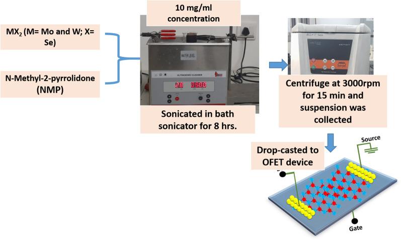
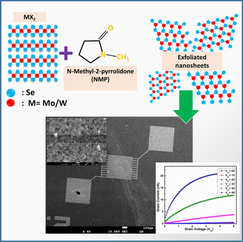
MoSe2 and WSe2 bulk powder (Alfa Aesar, 90% < 2 μm) and NMP (Sigma Aldrich) were used to synthesize the 2D-MoSe2 and WSe2 NSs by the LPE synthesis route because of their high yield and cost-effectiveness. In this process, we started with 10 mg/ml concentration of bulk powder in NMP in a glass vial. The prepared suspension was sonicated for 8 h in a bath sonicator. Once the sonication process was complete, the vials were left undisturbed overnight and solutions were centrifuged at 3000 rpm for 15 min. The supernatant was collected in glass vials. The supernatants were then investigated via various characterization techniques. The exfoliation of MoSe2 and WSe2 NSs can be understood by the schematic shown in Fig. 1. Hygroscopic and lactams have rich chemistry involving nucleophilic addition, elimination and ring interaction.33 For such processes, sonication is complemented by the presence of O2 and H2O from atmosphere. Thus, the extremely active intermediate species such as radicals or hyperoxides (in the case of NMP, N-methylsuccinimide [NMS] is created by auto-oxidation of NMP) promote the exfoliation. Some reports also suggest that auto-oxidation is triggered in the absence of sonication. It is supposed that the MX2 in NMP undergoes edge oxidation and partial dissolution which releases the highly charged anionic clusters. As a consequence, the negatively charged defects and anionic clusters are adsorbed on the surface of MX2, leading to the electrostatic repulsion of MX2 NSs in the colloids.34,35 Further, these 2D NSs were drop-cast on OFET chips (OFET Gen4 devices, Fraunhofer, Germany) to study their behavior as channel material. The source/drain is composed of gold with a thickness of 40 nm, separated by a 230-nm-thick dielectric layer of silicon dioxide (SiO2). Structural and morphological studies of the samples were carried out by 200 keV, high-resolution transmission electron microscopy (HR-TEM; JEOL JEM-F200 with a Gatan OneView camera), FESEM (JEOL, JSM-7610F), XRD (PANalytical Empyrean with Cu Kα as source λ = 1.54 Å), and Raman spectroscopy (Horiba Jobin–Yvon Labram HR system), respectively. The optical properties of the prepared samples were studied by UV–visible spectroscopy (UV-2401PC UV–visible spectrometer, Shimadzu). A four-probe setup (Keithley 2612A SourceMeter ) was used to measure the electrical properties of the FET device.
Fig. 1.
Schematic of synthesis process of MoSe2 and WSe2 nanosheets.
Results and Discussion
XRD Analysis
The XRD patterns of MoSe2 and WSe2 NSs are shown in Fig. 2. The peaks observed at 13.45 and 13.55 belong to the (002) Miller planes for MoSe2 and WSe2 NSs, respectively (JCPDS 98-004-9800 and 98-004-0752).29,36,37 The peak corresponding to 24 for both MoSe2 and WSe2 belongs to quartz. The peaks at 13.45 and 13.55 for MoSe2 and WSe2 NSs confirm that the synthesized NSs have a hexagonal 2H structure with space group P63/mmc which is semiconducting in nature.36 The broadness of (002) plane indicates the formation of a few-layer-thick layered material.38 The interplanar (d) spacing for the NSs is calculated for (002) plane using Bragg’s law:39
| 1 |
where d, and are the d-spacing, x-ray wavelength, and Bragg’s angle, respectively. The d-spacing for MoSe2 and WSe2 is 0.65 nm as calculated for the (002) plane, which is in good agreement with the values from the literature. The micro-strain values for the NSs were calculated using the following equation:40
| 2 |
where is the root mean square value of the micro-strain, β is the full width at half maximum (FWHM) and θ is the Bragg angle. The strain for MoSe2 and WSe2 is 4.22 and 1.62, respectively. The defect state created during the exfoliation process is responsible for the micro-strain produced in the MoSe2 and WSe2 structure, explained in the experimental section.
Fig. 2.
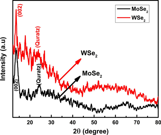
XRD pattern of MoSe2 and WSe2 nanosheet peaks at 13.45° and 13.55°, respectively, confirms the 2H phase.
TEM Analysis
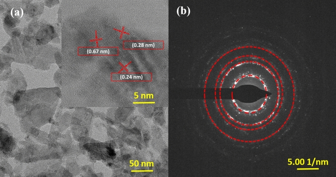
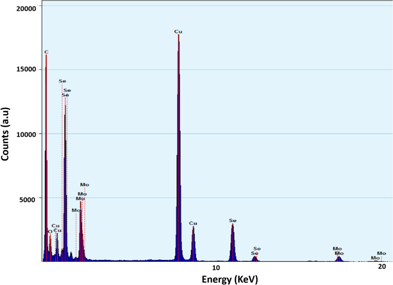
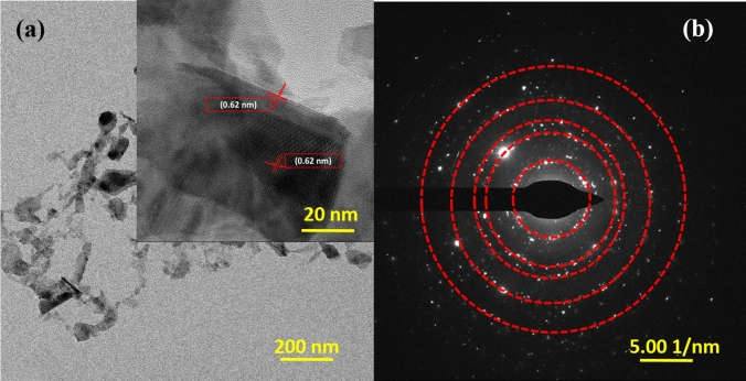
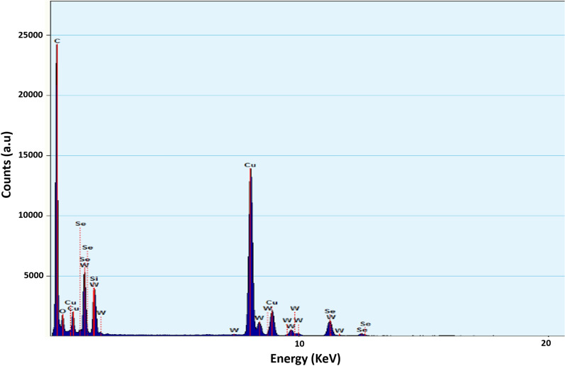
The morphology and internal structure of MoSe2 and WSe2 NSs were studied by TEM. For TEM measurement, suspension of MoSe2 and WSe2 NSs was drop-cast onto a carbon-coated copper grid. The TEM and selected area electron diffraction (SAED) patterns of MoSe2 and WSe2 NSs are shown in Figs. 3 and 4. The average lateral dimension of MoSe2 NSs is ~ 25 nm, which is shown in the inset of Fig. 3a. The zoomed image of the MoSe2 NSs is shown in Fig. 3b, and the d-spacing is calculated as 0.67 nm, 0.24 nm, and 0.28 nm, corresponding to the (002), (103), and (100) Miller planes, respectively.41–43 The TEM image of WSe2 NSs is shown in Fig. 5a, and the inset shows the image of the NS with interplanar spacing of 0.62 nm belonging to the (002) Miller plane, which matches with the XRD result.44 The average lateral dimension of WSe2 NSs is ~ 63 nm. The SAED pattern for MoSe2 and WSe2 is shown in Figs. 3b and 5b, respectively, and the circular diffraction pattern indicates that the NSs are polycrystalline in nature. The SAED pattern from multiple smaller grains may be responsible for the ring-like pattern, which was similarly reported for WS2 by Shinde et al.45 The energy-dispersive X-ray (EDX) spectra for MoSe2 and WSe2 are shown in Figs. 4 and 6, respectively, suggesting that there is no impurity present in the synthesized NS dispersion.
Fig. 3.
(a) TEM image and inset showing the HR-TEM image and (b) SAED pattern of MoSe2 NSs.
Fig. 4.
EDX spectra of MoSe2 NSs exfoliated in NMP.
Fig. 5.
(a) TEM image and inset showing the HR-TEM and (b) SAED pattern of WSe2 NSs.
Fig. 6.
EDX spectra of WSe2 NSs exfoliated in NMP.
Raman Analysis
Raman investigation of the MoSe2 and WSe2 NSs was carried out at 488 nm laser excitation, and three peaks observed in the range of 100–400 cm−1 were identified. The phonon modes were assigned by comparing the peaks with the existing literature. The 2H symmetry of MoSe2 and WSe2 belongs to the space group , and there are 12 modes of lattice vibration at the center of the Brillouin zone:46–48
| 3 |
where and are the acoustic mode, are the infrared-active modes, and,, are the Raman-active modes. These modes are divided into six pairs, where one is symmetric and the other is antisymmetric with respect to the inversion around the center lying around the Se-atom on both sides of the interlayer gap. The Raman spectra of MoSe2 and WSe2 NSs are shown in Fig. 7. The black line represents spectra of MoSe2, and the red line belongs to WSe2. The peaks observed at 169 cm−1, 241 cm−1, and 286 cm−1 are first-order Raman peaks assigned to phonon modes of MoSe2 corresponding to, , and . respectively, which match with the literature.46 The bulk is reported at 243 cm−1 in the literature, which is shifted to 2 cm−1 towards the lower wavenumber due to the decrease in interplanar restoring force.49 This also confirms the exfoliation of bulk MoSe2. Prominent Raman modes for WSe2 NSs were observed at 175 cm−1, 251 cm−1, and 282 cm−1 belonging to the, and , respectively.48,50 Similarly, the vibrational frequency for bulk WSe2 is reported at 253 cm−1,48 which is shifted by 2 cm−1 toward the lower wavenumber. The Raman spectra of MoS2 has been studied extensively to identify the thickness of NSs, whereas to the best of our knowledge, no such study has been reported for WSe2 and MoSe2 NSs that are thinner by a few layers.
Fig. 7.
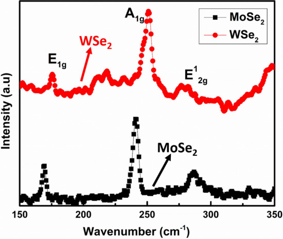
Raman spectra of MoSe2 and WSe2 nanosheets.
UV–Visible Spectroscopy
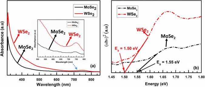
It is well known that the dimensionality affects the optical properties of materials. Therefore, absorption spectroscopy is used to study the optical properties of the synthesized NSs. The absorbance spectra of MoSe2 and WSe2 NSs are shown in Fig. 8a, and the zoomed-in image shows the absorbance peak of NSs. A broad peak in the region of 400–500 nm for both MoSe2 and WSe2 NSs can be attributed to the direct transition at the M-point of the Brillouin zone or due to the Van Hove singularity. The peaks at 741 nm and 748 nm for MoSe2 and WSe2 NSs, respectively, correspond to the direct excitonic transition at the K-point in the Brillouin zone. The direct bandgap of the NSs is calculated by using the Tauc equation given below:51,52
| 4 |
where α, hν, Eg, and A are the absorption coefficient, photo energy, bandgap, and constant, respectively. The bandgap energy of MoSe2 and WSe2 NSs is calculated by extrapolating the linear part of the Tauc plot []. The Tauc plot is shown in Fig. 8b. The bandgap values of MoSe2 and WSe2 NSs are 1.55 eV and 1.50 eV, respectively, which is higher than their bulk counterpart as reported in the literature.53,54 This difference in bandgap suggests that the bulk MoSe2 and WSe2 are reduced to few-layer-thick NSs.52
Fig. 8.
(a) Absorbance spectra of MoSe2 and WSe2 nanosheets, where the inset depicts the absorption peaks at 741 and 748 nm for MoSe2 and WSe2, respectively, (b) Tauc plots of MoSe2 and WSe2 nanosheets.
Electrical Properties of FET Devices
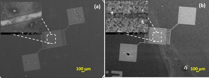
To investigate the electrical properties, the synthesized NSs were deployed as channel materials on a pre-patterned OFET substrate. The prepared NSs were drop-cast on the open-channel OFET devices with a channel length of 2.5 µm, as shown in Fig. 9a and b. The zoomed-in image of the channel confirms that MoSe2 and WSe2 NSs have been deposited over the channel.
Fig. 9.
(a, b) FESEM image of MoSe2 and WSe2 nanosheet channel-based FET devices.
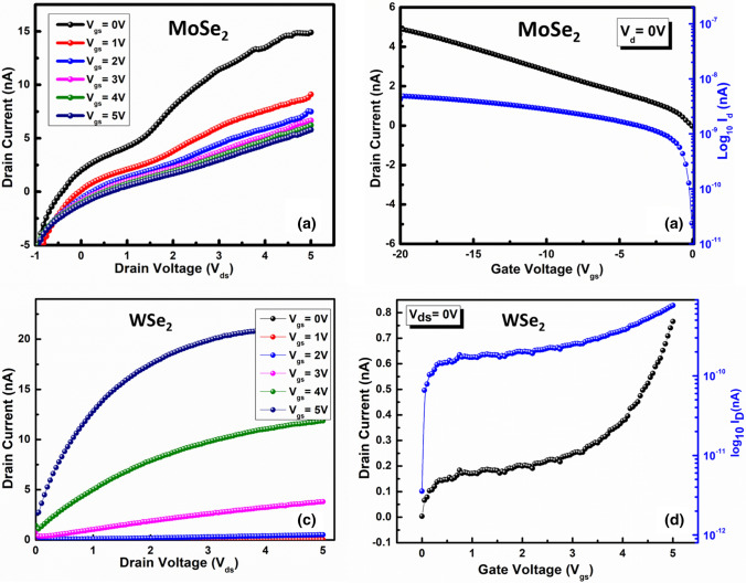
The devices were annealed at 473 K prior to electrical measurement in order to remove any residual contamination. The electrical measurement was performed on a Keithley 2612A SourceMeter in ambient atmosphere. The Au electrode acted as the source and drain electrode. The transfer and output characteristic curve of the MoSe2-FET is shown in Fig. 10a and b. Figure 10a confirms a linear relationship between the drain current and drain voltage up to −0.5 V (threshold voltage), indicating good ohmic contact between the Au electrode and MoSe2 channel material. In output characteristics, the Vgs varies from 0 V to 5 V. The drain current decreases with the application of gate voltage (Vgs) in the MoSe2 channel FET device. This decrease in drain current (increase in resistance) suggest that the depletion width increases for the MoSe2-FET device. When the applied voltage exceeds the threshold voltage, the device turns ON, and the current that flows through the channel in this situation is referred to as the ON current. The term “OFF current” refers to the current that exists below the threshold voltage, and it changes (increases) exponentially as the drain voltage increases. When the FET is in the OFF condition, there is no channel formed between the drain and source terminals. When the FET is in the other two regions, i.e. linear and saturation regions, it is in the ON condition, and there is a channel formed between the drain and source terminals. In transfer characteristics, the maximum ON current is 4.8 10−9 A and the OFF current is 2.37 10−11 A. The ON/OFF current ratio for the devices is 102. From the output characteristics of the WSe2-FET (shown in Fig. 10c), it is clear that there is a linear relationship between the channel material and the Au electrode. The saturation region is clearly visible in the output characteristics. The drain current increases with an increase in gate voltage, which suggests that upon application of the gate voltage there is an increase in the depletion width of the WSe2 FET device. This change in depletion width is responsible for the better FET performance. The transfer characteristics of the WSe2 FET device are shown in Fig. 10d. The maximum ON and OFF current for the WSe2-FET devices is 7.65 10−10 A and 3.55 10−12 A, respectively. The ON/OFF current ratio for the device is 102. The performance of the devices is on par matches with the reported literature.55–57 The FET parameters of both devices are given in Table I. This device fabrication approach could help researchers in the study of the TMD-FET for application in different types of sensors, such as gas sensors, biosensors, humidity sensors, photodetectors, and photovoltaic applications. The performance of the fabricated TMD FETs can be further enhanced by controlling the various processing issues including the generation of surface defects, presence of charge impurities, localized charge distribution, and trapped charges. Due to the presence of these defects, Coulomb scattering takes place, which causes high contact resistance between the metal and TMD material interface and hence overall degradation of device performance.
Fig. 10.
(a–d) Transfer and output characteristics of MoSe2 and WSe2 nanosheet channel-based FET devices.
Table I.
MoSe2 and WSe2 FET parameters derived from output and transfer characteristics
| S. No. | FET device | Threshold voltage (Vth) | ON current (A) | OFF current (A) | ON/OFF ratio |
|---|---|---|---|---|---|
| 1 | MoSe2-FET | −0.5 | 4.8 10−9 | 2.37 10−11 | 102 |
| 2 | WSe2-FET | −0.5 | 7.65 10−10 | 3.55 10−12 | 102 |
Conclusion
LPE was used to synthesize MoSe2 and WSe2 NSs, and these 2D-NSs were used as a channel material for FET applications. MoSe2 and WSe2 have a few-layer-thick 2H semiconducting phase. From Raman spectra, a vibration mode for MoSe2 and WSe2 exists, which confirms the reduction in the number of layers of 2D materials. From the UV–visible spectroscopy, we found that the bandgap values of MoSe2 and WSe2 NSs are 1.55 eV and 1.5 eV, respectively. These exfoliated NSs were cast off as the channel material for the OFET chips. A metal–semiconductor interface was formed at the contact and exhibited Schottky diode-like behavior, which is shown in the transfer characteristics of FET devices, and both devices exhibited n-type behavior. The electrical properties revealed that the ON/OFF current ratio for MoSe2 and WSe2 is 102. This approach for the fabrication of FET devices could advance the study of FET-based devices in sensing and photovoltaics.
Acknowledgments
The authors from Amity Institute of Nanotechnology (OPS and RS) acknowledge the financial support received from DRDO-SSPL (CARS-1115/CARS-64/TS/SPL/18), New Delhi, under the project. The authors are thankful to IUAC for extending the FESEM facility funded by the Ministry of Earth Sciences (MoES) under the Geochronology project [MoES/P.O.(Seismic)8(09)-Geochron/2012].
Conflict of interest
There are no conflicts to declare.
Footnotes
Publisher's Note
Springer Nature remains neutral with regard to jurisdictional claims in published maps and institutional affiliations.
References
- 1.Echtermeyer TJ, Lemme MC, Baus M, Szafranek BN, Geim AK, Kurz H. Nonvolatile switching in graphene field-effect devices. IEEE Electron Device Lett. 2008;29:952. doi: 10.1109/LED.2008.2001179. [DOI] [Google Scholar]
- 2.Kim DS, Nepal D, Geckeler KE. Individualization of single-walled carbon nanotubes: Is the solvent important? Small. 2005;1:1117. doi: 10.1002/smll.200500167. [DOI] [PubMed] [Google Scholar]
- 3.Yao Y, Lin Z, Li Z, Song X, Moon KS, Wong CP. Large-scale production of two-dimensional nanosheets. J. Mater. Chem. 2012;22:13494. doi: 10.1039/c2jm30587a. [DOI] [Google Scholar]
- 4.Novoselov KS, Geim AK, Morozov SV, Jiang D, Zhang Y, Dubonos SV, Grigorieva IV, Firsov AA. Electric field in atomically thin carbon films. Science. 2004;306:666. doi: 10.1126/science.1102896. [DOI] [PubMed] [Google Scholar]
- 5.Ahmad R, Srivastava R, Yadav S, Singh D, Gupta G, Chand S, Sapra S. Functionalized molybdenum disulfide nanosheets for 0D–2D hybrid nanostructures: photoinduced charge transfer and enhanced. J. Phys. Chem. Lett. 2017;8:1729. doi: 10.1021/acs.jpclett.7b00243. [DOI] [PubMed] [Google Scholar]
- 6.Pospischil A, Furchi MM, Mueller T. Solar-energy conversion and light emission in an atomic monolayer p-n diode. Nat. Nanotechnol. 2014;9:257. doi: 10.1038/nnano.2014.14. [DOI] [PubMed] [Google Scholar]
- 7.Das S, Kim M, Lee JW, Choi W. Synthesis, properties, and applications of 2-D materials: a comprehensive review. Crit. Rev. Solid State Mater. Sci. 2014;39:231. doi: 10.1080/10408436.2013.836075. [DOI] [Google Scholar]
- 8.Zhu J, Wang H, Ma L, Zou G. Observation of ambipolar photoresponse from 2D MoS2/MXene heterostructure. Nano Res. 2021;14(10):3416–3422. doi: 10.1007/s12274-021-3518-5. [DOI] [Google Scholar]
- 9.Anasori B, Lukatskaya MR, Gogotsi Y. 2D metal carbides and nitrides (MXenes) for energy storage. Nat. Rev. Mater. 2017 doi: 10.1038/natrevmats.2016.98. [DOI] [Google Scholar]
- 10.Jariwala D, Sangwan VK, Lauhon LJ, Marks TJ, Hersam MC. Emerging device applications for semiconducting two-dimensional transition metal dichalcogenides. ACS Nano. 2014;8:1102. doi: 10.1021/nn500064s. [DOI] [PubMed] [Google Scholar]
- 11.Chowdhury T, Sadler EC, Kempa TJ. Progress and prospects in transition-metal dichalcogenide research beyond 2D. Chem. Rev. 2020;120:12563. doi: 10.1021/acs.chemrev.0c00505. [DOI] [PubMed] [Google Scholar]
- 12.Yang Z, Zhang D, Wang D. Chemical carbon monoxide gas sensing properties of metal-organic frameworks-derived tin dioxide nanoparticles/molybdenum diselenide nanoflowers. Sens. Actuators B Chem. 2020;304:127369. doi: 10.1016/j.snb.2019.127369. [DOI] [Google Scholar]
- 13.Mueller T, Malic E. Exciton physics and device application of two-dimensional transition metal dichalcogenide semiconductors. NPJ 2D Mater. Appl. 2018 doi: 10.1038/s41699-018-0074-2. [DOI] [Google Scholar]
- 14.Li H, Lu G, Wang Y, Yin Z, Cong C, He Q, Wang L, Ding F, Yu T, Zhang H. Mechanical exfoliation and characterization of single- and few-layer nanosheets of WSe2, TaS2, and TaSe2. Small. 2013;9:1974. doi: 10.1002/smll.201202919. [DOI] [PubMed] [Google Scholar]
- 15.Bertolazzi S, Brivio J, Kis A. Stretching and breaking of ultrathin MoS2. ACS Nano. 2011;5:9703. doi: 10.1021/nn203879f. [DOI] [PubMed] [Google Scholar]
- 16.Song JG, Park J, Lee W, Choi T, Jung H, Lee CW, Hwang SH, Myoung JM, Jung JH, Kim SH, Lansalot-Matras C, Kim H. Layer-controlled, wafer-scale, and conformal synthesis of tungsten disulfide nanosheets using atomic layer deposition. ACS Nano. 2013;7:11333. doi: 10.1021/nn405194e. [DOI] [PubMed] [Google Scholar]
- 17.Zeng LH, Wu D, Lin SH, Xie C, Yuan HY, Lu W, Lau SP, Chai Y, Luo LB, Li ZJ, Tsang YH. Controlled synthesis of 2D palladium diselenide for sensitive photodetector applications. Adv. Func. Mater. 2019;29:1806878. doi: 10.1002/adfm.201806878. [DOI] [Google Scholar]
- 18.Duan X, Wang C, Pan A, Yu R, Duan X. Two-dimensional transition metal dichalcogenides as atomically thin semiconductors: opportunities and challenges. Chem. Soc. Rev. 2015;44:8859. doi: 10.1039/C5CS00507H. [DOI] [PubMed] [Google Scholar]
- 19.Kumara A, Ahluwalia PK. Electronic structure of transition metal dichalcogenides monolayers 1H-MX2 (M = Mo, W; X = S, Se, Te) from ab-initio theory: new direct band gap semiconductors. Eur. Phys. J. B. 2012;85:18. [Google Scholar]
- 20.Veeramalai CP, Li F, Liu Y, Xu Z, Guo T, Kim TW. Enhanced field emission properties of molybdenum disulphide few layer nanosheets synthesized by hydrothermal method. Appl. Surf. Sci. 2016;389:1017. doi: 10.1016/j.apsusc.2016.08.031. [DOI] [Google Scholar]
- 21.D. Sahoo, B. Singh, and B. Kaviraj, Strongly luminescent MoS2 nanosheets prepared by liquid phase exfoliation without any surfactant. in 3Rd international conference on condensed matter and applied physics (Icc-2019) 2220, 020027 (2020).
- 22.Kashyap PK, Kumar A, Srivastava R, Gupta S, Gupta BK. A Facile liquid phase exfoliation of tungsten diselenide using dimethyl sulfoxide as polar aprotic solvent to produce high-quality nanosheets. ChemNanoMat. 2021;7:328. doi: 10.1002/cnma.202100020. [DOI] [Google Scholar]
- 23.Kaur H, Yadav S, Srivastava AK, Singh N, Schneider JJ, Sinha OP, Agrawal VV, Srivastava R. Large area fabrication of semiconducting phosphorene by langmuir-blodgett assembly. Sci. Rep. 2016;6:34095. doi: 10.1038/srep34095. [DOI] [PMC free article] [PubMed] [Google Scholar]
- 24.Kaur H, Yadav S, Srivastava AK, Singh N, Rath S, Schneider JJ, Sinha OP, Srivastava R. High-yield synthesis and liquid-exfoliation of two-dimensional belt-like hafnium disulphide. Nano Res. 2018;11:343. doi: 10.1007/s12274-017-1636-x. [DOI] [Google Scholar]
- 25.H. Kaur, V. Varun Agrawal, and R. Srivastava, Unique morphologies of molybdenum disulphide: sheets, diffusion limited cluster aggregates and fractals, by langmuir-blodgett assembly for advanced electronics ArXiv Preprint ArXiv (2017).
- 26.Zhao W, Ghorannevis Z, Chu L, Toh M, Kloc C, Tan P, Eda G. Evolution of electronic structure in atomically thin sheets of WS2 and WSe2. ACS Nano. 2014;7:791. doi: 10.1021/nn305275h. [DOI] [PubMed] [Google Scholar]
- 27.Varghese S, Reig DS, Mehew JD, Block A, El Sachat A, Chávez-Ángel E, Sledzinska M, Ballesteros B, Sotomayor CM, Torres KJT. Fabrication and characterization of large-area suspended MoSe2 crystals down to the monolayer. J. Phys. Mater. 2021;4:046001. doi: 10.1088/2515-7639/ac2060. [DOI] [Google Scholar]
- 28.Fathi-Hafshejani P, Azam N, Wang L, Kuroda MA, Hamilton MC, Hasim S, Mahjouri-Samani M. Two-dimensional-material-based field-effect transistor biosensor for detecting COVID-19 Virus (SARS-CoV-2) ACS Nano. 2021;15:11461. doi: 10.1021/acsnano.1c01188. [DOI] [PubMed] [Google Scholar]
- 29.Jung C, Kim SM, Moon H, Han G, Kwon J, Hong YK, Omkaram I, Yoon Y, Kim S, Park J. Highly crystalline CVD-grown multilayer MoSe2 Thin film transistor for fast photodetector. Nat. Publ. Group. 2015;5:15313. doi: 10.1038/srep15313. [DOI] [PMC free article] [PubMed] [Google Scholar]
- 30.Yoo H, Hong S, Moon H, On S, Ahn H, Lee HK, Kim S, Hong YK, Kim JJ. Chemical doping effects on CVD-grown multilayer MoSe2 transistor. Adv. Electron. Mater. 2018;4:1. [Google Scholar]
- 31.Moon I, Choi MS, Lee S, Nipane A, Hone J, Yoo WJ. Analytical measurements of contact resistivity in two-dimensional WSe2 field-effect transistors. 2D Mater. 2021;8:045019. doi: 10.1088/2053-1583/ac1adb. [DOI] [Google Scholar]
- 32.Liu W, Kang J, Sarkar D, Khatami Y, Jena D, Banerjee K. Role of metal contacts in designing high-performance monolayer n-type WSe2 field effect transistors. Nano Lett. 2013;13:1983. doi: 10.1021/nl304777e. [DOI] [PubMed] [Google Scholar]
- 33.Grayfer ED, Kozlova MN, Fedorov VE. Colloidal 2D nanosheets of MoS2 and other transition metal dichalcogenides through liquid-phase exfoliation. Adv. Coll. Interface Sci. 2017;245:40. doi: 10.1016/j.cis.2017.04.014. [DOI] [PubMed] [Google Scholar]
- 34.Jawaid A, Nepal D, Park K, Jespersen M, Qualley A, Mirau P, Drummy LF, Vaia RA. Mechanism for liquid phase exfoliation of MoS2. Chem. Mater. 2016;28:337. doi: 10.1021/acs.chemmater.5b04224. [DOI] [Google Scholar]
- 35.Gupta A, Arunachalam V, Vasudevan S. Liquid-phase exfoliation of MoS2 nanosheets: the critical role of trace water. J. Phys. Chem. Lett. 2016;7:4884. doi: 10.1021/acs.jpclett.6b02405. [DOI] [PubMed] [Google Scholar]
- 36.Kirubasankar B, Vijayan S, Angaiah S. Sonochemical synthesis of a 2D–2D MoSe2 /graphene nanohybrid electrode material for asymmetric supercapacitors. Sustain. Energy Fuels. 2019;3:467. doi: 10.1039/C8SE00446C. [DOI] [Google Scholar]
- 37.Chakravarty D, Late DJ. Microwave and hydrothermal syntheses of WSe2 micro/nanorods and their application in supercapacitors. Dalton Trans. 2015;5:21700. [Google Scholar]
- 38.Balasingam SK, Lee JS, Jun Y. Few-layered MoSe2 nanosheets as an advanced electrode material for supercapacitors. Dalton Trans. 2015;44:15491. doi: 10.1039/C5DT01985K. [DOI] [PubMed] [Google Scholar]
- 39.Saxena N, Manzhi P, Choudhary RJ, Upadhyay S, Ojha S, Umapathy GR, Chawla V, Sinha OP, Krishna R. Performance optimization of transparent and conductive Zn1-xAlxO thin films for opto-electronic devices: an experimental & first-principles investigation. Vacuum. 2020;177:109369. doi: 10.1016/j.vacuum.2020.109369. [DOI] [Google Scholar]
- 40.Sharma R, Yadav K. Effect of lattice defects on the structural and optical properties of Ni1−XAgXO (where X = 0.0, 0.01, 0.03, 0.05, 0.10 and 0.15) nanoparticles. Appl. Phys. A. 2018 doi: 10.1007/s00339-017-1531-z. [DOI] [Google Scholar]
- 41.Chen Z, Liu H, Chen X, Chu G, Chu S, Zhang H. Wafer-size and single-crystal MoSe2 atomically thin films grown on GAn substrate for light emission and harvesting. ACS Appl. Mater. Interfaces. 2016;8:20267. doi: 10.1021/acsami.6b04768. [DOI] [PubMed] [Google Scholar]
- 42.Yuwen L, Zhou J, Zhang Y, Zhang Q, Shan J, Luo Z, Weng L, Teng Z, Wang L. Aqueous phase preparation of ultrasmall MoSe2 nanodots for efficient photothermal therapy of cancer cells. Nanoscale. 2016;8:2720. doi: 10.1039/C5NR08166A. [DOI] [PubMed] [Google Scholar]
- 43.Dai TJ, Liu YC, Fan XD, Liu XZ, Xie D, Li YR. Synthesis of few-layer 2H-MoSe2 thin films with wafer-level homogeneity for high-performance photodetector. Nanophotonics. 2018;7:1959. doi: 10.1515/nanoph-2018-0153. [DOI] [Google Scholar]
- 44.Fathipour S, Paletti P, Fullerton-Shirey SK, Seabaugh AC. Electric-double-layer p–i–n junctions in WSe2. Sci. Rep. 2020;10:1. doi: 10.1038/s41598-020-69523-9. [DOI] [PMC free article] [PubMed] [Google Scholar]
- 45.N. Babu Shinde, B. Deul Ryu, C. H. Hong, B. Francis, S. Chandramohan, and S. Kumar Eswaran, Growth Behavior, nucleation control and excellent optical properties of atomically thin WS2 thin films processed via Gas-phase chemical vapor deposition. Appl. Surf. Sci. 568, 150908 (2021).
- 46.Sekine T, Izumi M, Nakashizu T, Uchinokura K, Matsuura E. Raman scattering and infrared reflectance in 2H-MoSe2. J. Phys. Soc. Jpn. 1980;49:1069. doi: 10.1143/JPSJ.49.1069. [DOI] [Google Scholar]
- 47.Jin M, Zheng W, Ding Y, Zhu Y. Raman tensor of van der Waals MoSe2. J. Phys. Chem. Lett. 2020;11:4311. doi: 10.1021/acs.jpclett.0c01183. [DOI] [PubMed] [Google Scholar]
- 48.Luo X, Zhao Y, Zhang J, Toh M, Kloc C, Qihua Xiong S, Quek Y. Effects of lower symmetry and dimensionality on Raman spectra in two-dimensional WSe2. Phys. Rev. B. 2013 doi: 10.1103/PhysRevB.88.195313. [DOI] [Google Scholar]
- 49.Singh V, Late DJ, Goyal A, Rath S. Raman spectroscopic investigations of the selenization of MoO3 in the chemical vapor deposition process to form two-dimensional MoSe2. Appl. Surf. Sci. 2021;538:147946. doi: 10.1016/j.apsusc.2020.147946. [DOI] [Google Scholar]
- 50.Shi W, Lin M, Tan Q, Qiao X, Zhang J, Tan P. Raman and photoluminescence spectra of two-dimensional nanocrystallites of monolayer WS2 and WSe2. 2D Mater. 2016;3:025016. doi: 10.1088/2053-1583/3/2/025016. [DOI] [Google Scholar]
- 51.Sharma R, Kumar A, Kumari R, Garg P, Umapathy G, Laisharm R, Ojha S, Srivastava R, Sinha OP. A facile liquid-phase, solvent-dependent exfoliation of large scale MoS2 nanosheets and study of their photoconductive behaviour for UV-photodetector application. ChemistrySelect. 2021;6:11285. doi: 10.1002/slct.202102439. [DOI] [Google Scholar]
- 52.Zhang BQ, Chen JS, Niu HL, Mao CJ, Song JM. Synthesis of ultrathin WSe2 nanosheets and their high-performance catalysis for conversion of amines to imines. Nanoscale. 2018;10:20266. doi: 10.1039/C8NR05954C. [DOI] [PubMed] [Google Scholar]
- 53.Samikannu S, Sivaraj S. Dissipative soliton generation in an all-normal dispersion ytterbium-doped fiber laser using few-layer molybdenum diselenide as a saturable absorber. Opt. Eng. 2016;55:081311. doi: 10.1117/1.OE.55.8.081311. [DOI] [Google Scholar]
- 54.Wang K, Wu J, Chen G, Qiao H, Zhou Y, Li J, Qi X. A robust 3D self-powered photoelectrochemical type photodetector based on MoSe2 nanoflower. J. Mater. Sci.: Mater. Electron. 2021;32:14092. [Google Scholar]
- 55.Fan ZQ, Jiang XW, Chen J, Luo JW. Improving performances of in-plane transition-metal dichalcogenide schottky barrier field-effect transistors. ACS Appl. Mater. Interfaces. 2018;10:19271. doi: 10.1021/acsami.8b04860. [DOI] [PubMed] [Google Scholar]
- 56.Tosun M, Chuang S, Fang H, Sachid AB, Hettick M, Lin Y, Zeng Y, Javey A. High-gain inverters based on WSe2 complementary field-effect transistors. ACS Nano. 2014;8:4948. doi: 10.1021/nn5009929. [DOI] [PubMed] [Google Scholar]
- 57.Nazif KN, Kumar A, Hong J, Lee N, Islam R, Mcclellan CJ, Karni O, Van De Groep J, Heinz TF, Pop E, Brongersma ML, Saraswat KC. High-Performance p−n junction transition metal dichalcogenide photovoltaic cells enabled by MoOx doping and passivation. Nano Lett. 2021;21:3443–3450. doi: 10.1021/acs.nanolett.1c00015. [DOI] [PubMed] [Google Scholar]


