Abstract
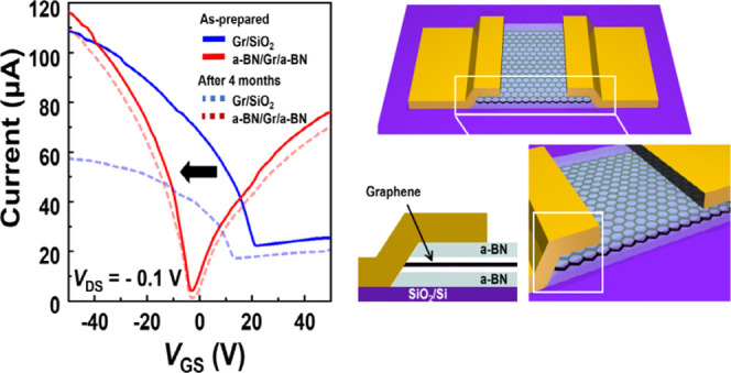
We successfully demonstrated the improvement and stabilization of the electrical properties of a graphene field effect transistor by fabricating a sandwiched amorphous boron nitride (a-BN)/graphene (Gr)/a-BN using a directly grown a-BN film. The a-BN film was grown via low-pressure chemical vapor deposition (LPCVD) at a low growth temperature of 250 °C and applied as a protection layer in the sandwiched structure. Both structural and chemical states of the as-grown a-BN were verified by various spectroscopic and microscopic analyses. We analyzed the Raman spectra of Gr/SiO2 and a-BN/Gr/a-BN structures to determine the stability of the device under exposure to ambient air. Following exposure, the intensity of the 2D/G-peak ratio of Gr/SiO2 decreased and the position of the G and 2D peaks red-shifted due to the degradation of graphene. In contrast, the peak position of encapsulated graphene is almost unchanged. We also confirmed that the mobility of a-BN/Gr/a-BN structure is 17,941 cm2/Vs. This synthetic strategy could provide a facile way to synthesize uniform a-BN film for encapsulating various van der Waals materials, which is beneficial for future applications in nanoelectronics.
Keywords: amorphous boron nitride (a-BN), graphene, heterojunction, field effect transistor (FET), high mobility, boron nitride encapsulation
Introduction
Graphene has been widely used in a variety of applications, such as in field effect transistors (FETs) and memory and tunneling devices, because of its superior electrical properties.1−6 However, graphene has a limitation in that all its carbon atoms are exposed to the external environment, which could cause performance degradation of graphene-based devices.7−9 After exposure to the external environment, silanol groups on the SiO2 surface interfere with the movement of charge carriers, resulting in localized charge accumulation at the interface between graphene and SiO2.10−12 Numerous approaches have been introduced to enhance the stability and performance of graphene-based devices.13−15 Encapsulating such devices using various 2D materials (2DMs) can prevent their deterioration due to external effects.16−21 In particular, hexagonal boron nitride (h-BN) films have many advantageous properties such as a large band gap of approximately 6 eV, and a dielectric constant of ∼3.76. h-BN films have the same hexagonal atomic structure and high crystallinity as 2DMs; thus, they can improve mobility and stabilize device performance (Table S1).18−21 Several research groups have demonstrated the large-scale growth of h-BN on metal catalytic substrates;22−24 however, because of the wet-etching process of metal catalysts during stacking with other 2DMs, contamination at the interface is inevitable.25 In addition, to obtain an h-BN film with a large area, a high growth temperature and a long growth time are required. As an alternative for the crystalized h-BN, amorphous boron nitride (a-BN) has been considered a promising encapsulating material for 2DMs because it is relatively free of defects (traps and dangling bonds) and requires low growth temperature.26−31 Glavin et al. and Hong et al. explored the dielectric properties of ultrathin a-BN film and diffusion barrier behavior for ultrathin electronic devices.28,29 Uddin et al. confirmed that FETs of graphene on an a-BN heterointerface could enhance the hole and electron mobilities to 4980 and 4200 cm2/Vs, respectively.30 Very recently, Lu et al. verified that a-BN film successfully suppresses current fluctuations and enhances carrier mobility of 2D materials.31 However, fabricating a-BN films still has several issues, such as the requirement of additional annealing processes at relatively high temperatures, complicated processes for making the protection layer, and the debate over the transfer process. Above all, experiments to confirm whether a-BN can sufficiently protect 2D materials from the external environment and help improve electrical performance have not been appropriately explored or performed yet (Table S2).
In this study, we succeeded in growing centimeter-sized uniform a-BN films on arbitrary substrates (e.g., graphene/Ge substrate and SiO2/Si substrate) at a low temperature. Using X-ray photoemission spectroscopy (XPS), Raman spectroscopy, and high-resolution transmission electron microscopy (HR-TEM), we verified the high disorderness and near-stoichiometry of the BN film. A capacitance–voltage (C–V) analysis was performed to evaluate the electrical properties of the as-grown a-BN film, and the dielectric constant of a-BN was approximately 1.25 at 1 MHz, very close to the κ of air. Since the a-BN film could be directly grown on the graphene/Ge substrate, we assembled a-BN/graphene/a-BN heterostructure without a wet-etching transfer process. Notably, we fabricated FET-based a-BN-encapsulated graphene and confirmed the enhancement of both stability and transport properties, even after 4-month of exposure to ambient air conditions.
Experimental Details
Low-Temperature Growth of a-BN on an Arbitrary Substrate
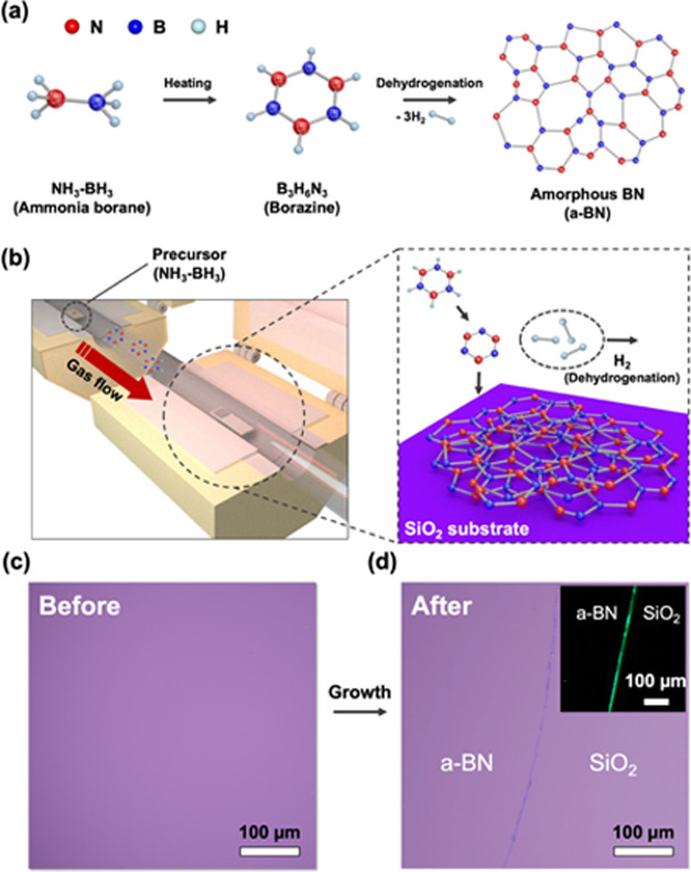
a-BN films were synthesized using a 2-inch double-zone low-pressure chemical vapor deposition system, which was divided into a precursor-vaporization zone (furnace 1) and a reaction zone (furnace 2) (Figure 1). First, ammonia–borane complex (NH3-BH3, 97% purity, 10 mg, Sigma-Aldrich) powder and arbitrary substrates of 1.5 × 1.5 cm2 size (graphene/Ge substrate or 300 nm SiO2/Si substrate) were loaded into furnaces 1 and 2, respectively. The detailed protocol for the growth of graphene on the Ge substrate is described in Figure S1 in the Supplementary Information.32 The chamber was evacuated to a high vacuum (∼1 mTorr) for 30 min. Then, furnace 2 was heated to 250 °C while maintaining 110 Torr at a flow of 20 sccm of H2 (99.999%) and furnace 1 was heated to 100 °C for 30 min to form dehydrogenated B3N6H3 molecules. Simultaneously, evaporated B3N6H3 molecules begin to deposit on the substrate in furnace 2 (Figure 1b). After obtaining the a-BN film of the desired thickness, both furnaces were cooled to room temperature to avoid further growth. Figure 1c,d shows OM images of a 300 nm SiO2/Si substrate before and after a-BN growth, which indicates that the as-grown a-BN is uniform and transparent (surface morphology and average thickness of a-BN is described in Figure S2).27
Figure 1.
Schematic illustration of the (a) growth mechanism of the a-BN film and (b) double-zone low-pressure chemical vapor deposition system. The solid-phase precursor vaporizes in furnace 1 and is supplied into furnace 2. Optical microscopic (OM) images of 300 nm SiO2/Si substrates (c) before and (d) after a-BN growth. (Inset) Dark-field OM image apparently shows the synthesized a-BN on 300 nm SiO2/Si.
Encapsulation and Device Fabrication
Both encapsulation and device fabrication processes are schematically described in Figure S3a. We deposited a 40 nm Au film on an a-BN film-coated graphene/Ge substrate (a-BN/Gr/Ge) through thermal evaporation. Then, poly(methyl methacrylate) (PMMA) solution (PMMA A4, 4% by weight of PMMA in anisole) was spin-coated on the samples at 2500 rpm for 60 s and samples were baked at 120 °C for 10 min. Consequently, a thermal release tape (TRT) was attached, and a mechanical exfoliation method was used to separate a-BN/Gr from the Ge substrate. The stacked TRT/PMMA/Au film/a-BN/Gr structure was transferred onto an a-BN/SiO2/Si substrate using a thermal press at 100 °C for 5 min. After detaching TRT at 120 °C, PMMA was removed using hot (50 °C) acetone treatment for 1 h and dipping in isopropyl alcohol to remove any residual PMMA. The Au film was removed using potassium iodide/iodine (KI/I2) solution. The two-terminal device structure was patterned by standard photolithography (width: 2.0 μm and length: 3.0 μm). To expose the graphene edge, patterned a-BN regions were etched away using plasma etching (a mixture of 10 sccm of Ar and SF6 at 100 W for 2 min). A thermal evaporator was used to deposit 15 nm Cr and 85 nm Au metals as metal electrodes for the source and drain of the FET devices. To compare the performance of the device, we prepared a graphene-based FET device on a 300 nm SiO2/Si substrate (Figure S3b).
Characterization
HR-TEM analysis was performed using a Seron AIF 2100 (Philips CM30). Film thickness was characterized by HR-TEM and atomic force microscopy (AFM, scan rate: 0.5 Hz, Park NX10, Park System). Raman spectroscopy (Alpha300 M+, WITec GmbH) with an excitation wavelength of 532 nm and a Nd:YLF laser was used to investigate the crystal properties of the samples (graphene and a-BN film for a laser power of 5 and 30 mW, respectively). The chemical composition of amorphous boron nitride and graphene were determined by XPS using an ESCA2000 spectrometer; a-BN (power = 120 W, calibration peak: C 1s with a peak at around 284.8 eV) and graphene (power = 80 W, calibration peak: C 1s with a peak at about 284.6 eV). A Keithley 2400 was used to measure the I–V characteristics of both types of graphene FET devices at room temperature (compliance: 0.01 A and scan step: 0.1 V). The capacitance–voltage (C–V) characteristics of the Ag/a-BN/Si/Ag configuration were measured using a K4200A-SCS parameter analyzer system and a probe station facility at room temperature under ambient conditions. The top and bottom electrodes with thicknesses of 100 nm were deposited on a-BN and Si.
Results and Discussion
Chemical and Electrical Properties of the a-BN Film
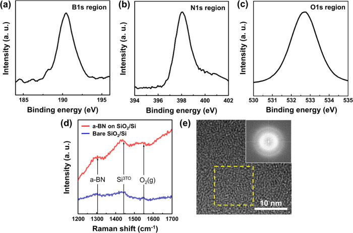
The elemental composition of the a-BN film was analyzed by XPS. High-resolution XPS scans of the B 1s and N 1s depicted single distributed boron and nitrogen atomic bonds, with peaks at 190.4 and 398.1 eV, respectively (Figure 2a,b).29 The peak locations and lack of secondary peaks indicate very low levels of impurities in the a-BN film. Surface oxidation can hinder the encapsulation of the a-BN layer and is commonly reported in BN films.33 However, oxidation peaks (around 192.1 eV) were absent in the XPS spectrum, indicating that the a-BN thin film surface was not oxidized. Figure 2b shows almost no fingerprint of metallic B–B bonding, which appears at B 1s ≈ 187 eV. Additionally, the ratio of B to N was nearly 1 to 1, demonstrating stoichiometric a-BN thin film growth. As shown in Figure 2c, the O 1s peak was observed at 532.7 eV, originating from the bottom SiO2/Si substrate. Compared to the O 1s peak of bare SiO2/Si substrate, the hydroxyl groups on the SiO2 surface were almost eliminated during a-BN film growth, indicating that the as-grown a-BN film well passivated the hydrophilic SiO2 surface (Figure S4).34
Figure 2.
(a–c) N 1s, B 1s, and O 1s region in XPS profiles for the a-BN film on a 300 nm SiO2/Si substrate. (d) Raman spectra acquired from the as-grown a-BN film on a 300 nm SiO2/Si substrate (red) and bare 300 nm SiO2/Si substrate (blue). (e) HR-TEM image of the a-BN film. The inset image shows a fast Fourier transform results of the area depicted in the yellow box inside Figure 2e, indicating a disordered arrangement.
Raman spectroscopy was performed to check the noncrystalline state of the a-BN film on the SiO2/Si substrate. As shown in Figure 2d, the a-BN samples exhibit an amorphous growth status compared to bare SiO2/Si. Three peaks were observed from 1200 to 1700 cm–1 for the a-BN film. The small peak near 1300 cm–1 is ascribed as E2g vibrational mode of BN, which has been shifted to a lower wave number from the peak position of hybridized BN with sp2 bonds at around 1370 cm–1.35−37 This large shift might be due to the random strain effect dominating the degradation of the crystal structure.36−38 The broad peaks at 1450 and 1550 cm–1 were assigned to the third-order transverse optical phonon originating from the Si substrate and the molecular oxygen (e.g., ambient oxygen), respectively.37,38 We analyzed the as-grown a-BN films using top-view TEM images (Figure 2e) to prove the noncrystalline structure and electron diffraction patterns of the grown BN films and found the absence of long-range atomic order (refer to the amorphous nature of BN).
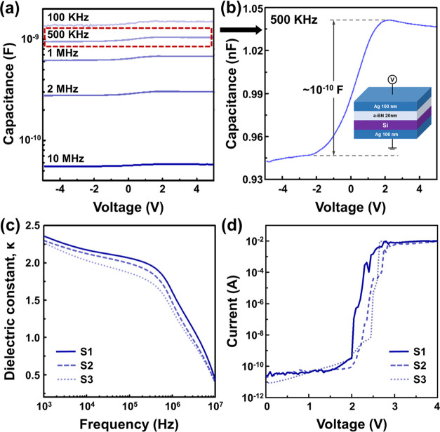
To verify the electrical properties of the as-grown a-BN, we prepared three samples with the Ag/a-BN/Si/Ag configuration (Figure 3). The thickness of a-BN was 20.4 nm for all samples (Figure S5). The capacitance value decreased by more than 1 order of magnitude when the applied frequency was increased from 100 kHz to 10 MHz (Figure 3a). For instance, the capacitance at 3 V was reduced from 5.8 × 10⁻¹¹ to 1.48 × 10⁻⁹ F, when the frequency was increased to 10 MHz. The magnified view of capacitance shows that capacitance increases as a function of voltage (see Figure 3b) for a frequency of 500 kHz. The relative dielectric constants (κ) of a-BN at different frequencies are shown in Figure 3c. At 1 kHz, the κ value was approximately 2.3, and it decreased to approximately 0.4 at 10 MHz, which is close to the findings reported in the literature.39,40 Significantly, the κ value for a-BN was approximately 1.25 at 1 MHz, very close to the κ of air. This low κ value is probably due to the absence of crystalline order in the a-BN structure, which hinders the dipole alignment.19 The I–V characteristics of the a-BN film are shown for the three samples in vertical electrode configurations (Figure 3d). The current increased gently up to approximately 2 V (Poole–Frenkel tunneling) and then dramatically enhanced due to leakage current flow, resulting in an electrical breakdown in the sample at approximately 2.6 V.
Figure 3.
(a) Capacitance as a function of voltage, (b) maximized figure of capacitance changes via voltage, (c) relative dielectric constant versus frequency, and (d) I–V characteristics of a-BN samples.
a-BN/Graphene/a-BN Encapsulation
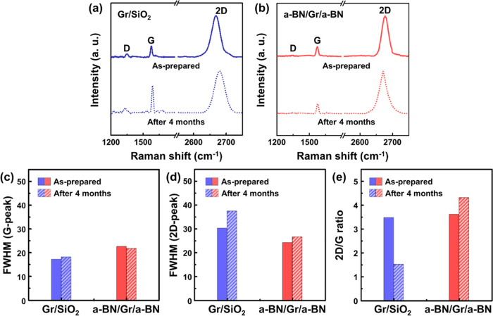
Owing to its ultrathin layers, the structural morphology of graphene is severely affected by the substrate, resulting in different degrees of local structure.41 Furthermore, it has been proven that SiO2 substrates may facilitate the facile degradation of monolayer graphene under ambient conditions by reducing its stability against oxidation.42 These ambient-related factors modify the transport properties, such as graphene’s carrier mobility and conductance. Here, we fabricated sandwiched a-BN/Gr/a-BN structures on a SiO2/Si substrate for the stability of the channel layer, which was then exposed to ambient air for 4 months. Figure 4a,b presents the Raman spectra of a-BN/Gr/a-BN compared to those of Gr/SiO2 before and after exposure to ambient air. Three peaks were identified: the D-peak at approximately 1350 cm–1 comes from transverse optical phonons around the Brillouin zone corner K, the G-peak at approximately 1580 cm–1 originates from the emission of zone-center optical phonons (in-plane phonon mode), and the 2D-peak at approximately 2700 cm–1 corresponds to the high-energy second-order process, which was induced by preferential coupling to transverse optical phonons near the edge of the Brillouin zone.43−45
Figure 4.
Raman spectra analysis for (a) Gr/SiO2, and (b) a-BN/Gr/a-BN samples; as prepared and after 4 months. Calculated full width at half-maximum for (c) G-peak and (d) 2D-peak. (e) Value of 2D/G compared in as prepared and after 4 months.
In the case of Gr/SiO2 as a channel layer, both G-peak and 2D-peak were red-shifted and broadened at the same time after exposure to the ambient air: The peak position of G and 2D peaks at 1577.9 and 2669.2 cm–1 changed to 1588.7 and 2680.6 cm–1, respectively, and the full width at half-maximum (FWHM) values of the G and 2D peaks increased from 17.1 and 30.2 cm–1 to 18.14 and 37.4 cm–1, respectively (Figure 4c,d). A redshift is an increase in wavenumber, with a corresponding decrease in the frequency of an electromagnetic wave, which means that the frequency of phonons interacting with the incident photon decreases.46,47 Ambient conditions and the adsorption of molecules, such as O2, on the surface of graphene vary the chemical interactions, thus altering the peak position and width in the Raman spectrum.48 Furthermore, we observed that the peak ratio of G and 2D peaks ratio of the Gr/SiO2 samples decreased to 1.5 from its initial value of approximately 3.5. Thus, we believe that when the graphene is exposed to ambient air, disordering and oxidation of the graphene can occur, increasing the concentration of charged impurities in the graphene.49−52 On the contrary, when the graphene is perfectly encapsulated by the a-BN (a-BN/Gr/a-BN structure), we confirmed that the width of the peaks has narrowed compared to those of the Gr/SiO2 sample and there is little change in the Raman spectrum after 4 months of exposure to ambient air. Although the peak position of 2D slightly shifted by around 4 cm–1, there was no change in the 2D/G ratio and FWHM values, indicating that the quality of graphene has not degraded.
Device Stability of Field Effect Transistor (FET)
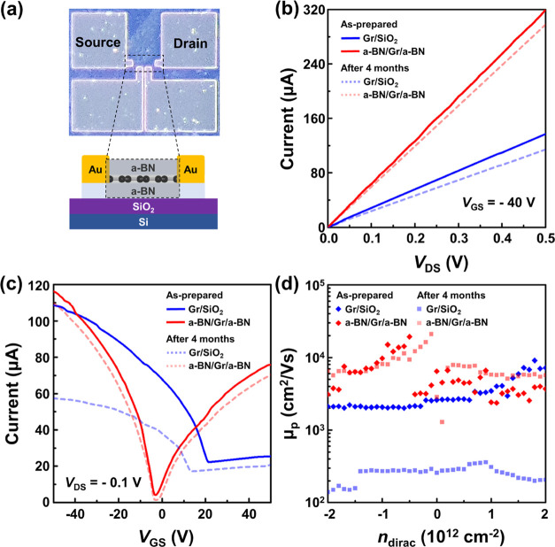
Figure 5a shows the top view of the optical microscope image of FET devices with a sandwiched a-BN/Gr/a-BN structure and its electrical properties based on the FET device. The ID–VDS curves of the two samples (FETs based on a-BN/Gr/a-BN and Gr/SiO2) were evaluated. The current level of Gr/SiO2 was 137 μA (a-BN/Gr/a-BN: 319 μA) at VDS = 0.5 V. After 4 months, the current level of both a-BN/Gr/a-BN and Gr/SiO2 samples were decreased to 114 and 297 μA, respectively. The a-BN/Gr/a-BN FET device can be operated at a significantly higher ID than that of the graphene FET (GFET) on the SiO2 substrate, as shown in Figure 5b. Furthermore, no hysteresis effect was observed in a-BN-encapsulated FET devices, probably because of the clean graphene/a-BN interface and the absence of adsorbed impurities on the GFET channel surface.53Figure 5c shows the transfer curves (ID–VGS) of the GFET devices. The results demonstrate that the device performance of the sandwiched a-BN/Gr/a-BN structure reached a positive neutrality point voltage (VNP) around −2 V, which resulted in fewer charge traps. This leads to enhanced electron flow owing to the surface dielectric screening effect.54 For the Gr/SiO2 FET, the neutrality point voltage shifted to 12.5 V, which is mainly attributed to the dopants adsorbed on the graphene surface owing to its storage under relatively humid ambient conditions. As shown in Figure 5d, we extracted the field effect mobility (μFE) to compare the device performances of the sandwiched structure of the FET device to that of the Gr/SiO2 structure using the following equation55
where L, W, VDS, and VGS are the channel length, channel width, drain-source voltage, and gate-source voltage, respectively, and the capacitance per unit area (C) is ε0ε/d, with relative permittivities of 4 and 2 for SiO2 and a-BN, respectively. For the Gr/SiO2 FET device (Figure 5d), the field effect mobility around the low-carrier-density regime (n ≈ 0.1 × 1012 cm–2) was approximately 698 cm2/Vs, whereas that of a-BN-encapsulated FET was 17,941 cm2/Vs, resulting in an approximately 26-fold enhancement in carrier mobility. We conclude that the electrical properties of the graphene channel a-BN can be effectively improved and it can be protected from degradation under external environmental exposure.
Figure 5.
Optical microscope image of FET device structure of (a) Gr/SiO2 and a-BN/Gr/a-BN, (b) drain current (ID) with drain-source voltage (VDS) curves, (c) transfer curves ID-gate-source (VGS) of two samples, (d) field effect mobility for two samples of as prepared and after 4 months.
Conclusions
In summary, we successfully synthesized large-area a-BN films at a low temperature of 250 °C and performed optical, chemical, structural, and electrical analyses. Chemical analysis revealed that our a-BN film has sp2-bonded B and N. a-BN films have been synthesized for various applications and can be used to fabricate sandwich structures via dry exfoliation transfer processes. We analyzed the a-BN film and stability of the a-BN/Gr/a-BN structure compared to the Gr/SiO2 structure and fabricated FET devices to improve the field effect mobility. The μFE of a-BN/Gr/a-BN was better than that of Gr/SiO2, achieving a value of 21,000 cm2/Vs. Also, the current of the Gr/SiO2 structured FET device was 114 μA at VDS = 0.5 V, compared to 297 μA for the a-BN/Gr/a-BN structured FET device. We believe that our study of FET devices with a sandwiched a-BN/Gr/a-BN structure will be helpful for applications in future nanoelectronics based on ultrathin vdW materials.
Acknowledgments
This research was supported by the National Research Foundation (NRF) fund of Korea (NRF-2021R1A2C2012649, and NRF-2021M3H1A104892211) and by the Ajou University research fund. The authors are thankful for the help of Prof. M. Kim from Seoul National University.
Glossary
Abbreviations
- a-BN
amorphous boron nitride
- Gr
graphene
- FET
field effect transistor
- LPCVD
low-pressure chemical vapor deposition
- 2DMs
2D materials
- h-BN
hexagonal boron nitride
- OM
optical microscope
- HR-TEM
high-resolution TEM
- AFM
atomic force microscopy
- XPS
X-ray photoelectron spectroscopy
- I–V
current–voltage
- C–V
capacitance–voltage
- TO
transverse optical
- FWHM
full width at half-maximum
- GFETs
graphene FETs
- VNP
neutrality point voltage
- μFE
field effect mobility
Supporting Information Available
The Supporting Information is available free of charge at https://pubs.acs.org/doi/10.1021/acsami.2c18706.
Detailed information on the growth of single-crystal graphene on Ge substrate, thickness and uniformity of a-BN, encapsulation and device fabrication process, and the O 1s spectrum of bare SiO2/Si substrate (PDF)
The authors declare no competing financial interest.
Supplementary Material
References
- Novoselov K. S.; Fal’ko V. I.; Colombo L.; Gellert P. R.; Schwab M. G.; Kim K. A roadmap for graphene. Nature 2012, 490, 192–200. 10.1038/nature11458. [DOI] [PubMed] [Google Scholar]
- Dean C. R.; Wang L.; Maher P.; Forsythe C.; Ghahari F.; Gao Y.; Katoch J.; Ishigami M.; Moon P.; Koshino M.; Taniguchi T.; Watanabe K.; Shepard K. L.; Hone J.; Kim P. Hofstadter’s Butterfly and The Fractal Quantum Hall Effect in Moiré Superlattices. Nature 2013, 497, 598–602. 10.1038/nature12186. [DOI] [PubMed] [Google Scholar]
- Bandurin D.-A.; Svintsov D.; Gayduchenko I.; Xu S-G.; Principi A.; Moskotin M.; Tretyakov I.; Yagodkin D.; Zhukov S.; Taniguchi T.; Watanabe K.; Grigorieva I.-V.; Polini M.; Goltsman G.-N.; Geim A.-K.; Fedorov G. Resonant Terahertz Detection using Graphene Plasmons. Nat. Commun. 2018, 9, 5392 10.1038/s41467-018-07848-w. [DOI] [PMC free article] [PubMed] [Google Scholar]
- Withers F.; Del Pozo-Zaumdio O.; Mishchenko A.; Rooney A. P.; Gholinia A.; Watanabe K.; Taniguchi T.; Haigh S. J.; Geim A. K.; Tarakovskii A. I.; Novoselov K. S. Light-emitting diodes by band-structure engineering in van der Waals heterostructures. Nat. Mater. 2015, 14, 301–306. 10.1038/nmat4205. [DOI] [PubMed] [Google Scholar]
- Hong A. J.; Song E. B.; Yu H. S.; Allen M. J.; Kim J.; Fowler J. D.; Wassei J. K.; Park Y.; Wang Y.; Zou J.; Kaner R. B.; Weiller B. H.; Wang K. L. Graphene Flash Memory. ACS Nano 2011, 5, 7812–7817. 10.1021/nn201809k. [DOI] [PubMed] [Google Scholar]
- Moon J. Y.; Kim M.; Kim S. I.; Xu S.; Choi J. H.; Whang D.; Watanabe K.; Taniguchi T.; Park D. S.; Seo J.; Cho S. H.; Son S. K.; Lee J. H. Layer-engineered large-area exfoliation of graphene. Sci. Adv. 2020, 6, eabc6601 10.1126/sciadv.abc6601. [DOI] [PMC free article] [PubMed] [Google Scholar]
- Some S.; Kim J.; Lee K.; Kulkarni A.; Yoon Y.; Lee S.; Kim T.; Lee H. Highly Air-Stable Phosphorus-Doped n-Type Graphene Field-Effect Transistors. Adv. Mater. 2012, 24, 5481–5486. 10.1002/adma.201202255. [DOI] [PubMed] [Google Scholar]
- Alexandrou K.; Petrone N.; Hone J.; Kymissis I. Encapsulated Graphene Field-Effect Transistors for Air Stable Operation. Appl. Phys. Lett. 2015, 106, 113104 10.1063/1.4915513. [DOI] [Google Scholar]
- Hayasaka T.; Kubota Y.; Liu Y.; Lin L. The Influences of Temperature, Humidity, and O2 on Electrical Properties of Graphene FETs. Sens. Actuators, B 2019, 285, 116–122. 10.1016/j.snb.2019.01.037. [DOI] [Google Scholar]
- Calizo I.; Teweldebrhan D.; Bao W.; Miao F.; Lau C. N.; Balandin A. A. Spectroscopic Raman Nanometrology of Graphene and Graphene Multilayers on Arbitrary Substrates. J. Phys.: Conf. Ser. 2008, 109, 012008 10.1088/1742-6596/109/1/012008. [DOI] [Google Scholar]
- Nagashio K.; Yamashita T.; Nishimura T.; Kita K.; Toriumi A. Electrical Transport Properties of Graphene on SiO2 with Specific Surface Structures. J. Appl. Phys. 2011, 110, 024513 10.1063/1.3611394. [DOI] [Google Scholar]
- Entani S.; Takizawa M.; Li S.; Naramoto H.; Sakai S. Growth of Graphene on SiO2 with Hexagonal Boron Nitride Buffer Layer. Appl. Surf. Sci. 2019, 475, 6–11. 10.1016/j.apsusc.2018.12.186. [DOI] [Google Scholar]
- Logoteta D.; Fiori G.; Lannaccone G. Graphene-Based Lateral Heterostructure Transistors Exhibits Better Intrinsic Performance than Graphene-Based Vertical Transistors as Post-CMOS Devices. Sci. Rep. 2014, 4, 6607 10.1038/srep06607. [DOI] [PMC free article] [PubMed] [Google Scholar]
- Liu J.-j.; Li R.; Li Y.; Li H.; Yi J.; Wang H.; Zhao X.; Liu P.; Guo J.; Liu L. Graphene-Based in-Plane Heterostructures for Atomically Thin Electronics. New Carbon Mater. 2018, 33, 481. 10.1016/S1872-5805(18)60352-X. [DOI] [Google Scholar]
- Zhang Z.; Lin P.; Liao Q.; Kang Z.; Si H.; Zhang Y. Graphene-Based Mixed-Dimensional Van Der Waals Heterostructures for Advanced Optoelectronics. Adv. Mater. 2019, 31, 1806411 10.1002/adma.201806411. [DOI] [PubMed] [Google Scholar]
- Kim T.; Fan S.; Lee S.; Joo M.-J.; Lee Y. H. High-Mobility Junction Field-Effect Transistor via Graphene/MoS2 Heterointerface. Sci. Rep. 2020, 10, 13101 10.1038/s41598-020-70038-6. [DOI] [PMC free article] [PubMed] [Google Scholar]
- Low C. G.; Zhang Q.; Hao Y.; Ruoff R. S. Graphene Field Effect Transistors with Mica as Gate Dielectric Layers. Small 2014, 10, 4213. 10.1002/smll.201303929. [DOI] [PubMed] [Google Scholar]
- Dean C. R.; Young A. F.; Meric I.; Lee C.; Wang L.; Sorgenfrei S.; Watanabe K.; Taniguchi T.; Kim P.; Shepard K. L.; Hone J. Boron Nitride Substrates for High Quality Graphene Electronics. Nat. Nanotechnol. 2010, 5, 722–726. 10.1038/nnano.2010.172. [DOI] [PubMed] [Google Scholar]
- Laturia A.; Van de Put M. L.; Vandenberghe W. G. Dielectric properties of hexagonal boron nitride and transition metal dichalcogenides: from monolayer to bulk. npj 2D Mater. Appl. 2018, 2, 6. 10.1038/s41699-018-0050-x. [DOI] [Google Scholar]
- Illarionov Y. Y.; Knobloch T.; Jech M.; Lanza M.; Akinwande D.; Vexler M. I.; Mueller T.; Lemme M. C.; Fiori G.; Schwierz F.; Grasser T. Insulator for 2D nanoelectronics: The Gap to Bridge. Nat. Commun. 2020, 11, 3385 10.1038/s41467-020-16640-8. [DOI] [PMC free article] [PubMed] [Google Scholar]
- Zhang J.; Tan B.; Zhang X.; Gao F.; Hu Y.; Wang L.; Duan X.; Yang Z.; Hu P. Atomically Thin Hexagonal Boron Nitride and its Heterostructures. Adv. Mater. 2020, 33, 2000769. 10.1002/adma.202000769. [DOI] [PubMed] [Google Scholar]
- Jeong H.; Kim D. Y.; Kim J.; Moon S.; Han N.; Lee S. H.; Okello O. F. N.; Song K.; Choi S.-Y.; Kim J. K. Wafer-Scale and Selective-Area Growth of High-Quality Hexagonal Boron Nitride on Ni (111) by Metal-Organic Chemical Vapor Deposition. Sci. Rep. 2019, 9, 5736 10.1038/s41598-019-42236-4. [DOI] [PMC free article] [PubMed] [Google Scholar]
- Oh H.; Jo J.; Tchoe Y.; Yoon H.; Lee H. H.; Kim S.-S.; Kim M.; Sohn B.-H.; Yi G.-C. Centimeter-Sized Epitaxial h-BN Films. NPG Asia Mater. 2016, 8, e330 10.1038/am.2016.178. [DOI] [Google Scholar]
- Song L.; Ci L.; Lu H.; Sorokin P. B.; Jin C.; Ni J.; Kvashnin A. G.; Kvashnin D. G.; Lou J.; Yakobson B. I.; Ajayan P. M. Large Scale Growth and Characterization of Atomic Hexagonal Boron Nitride layers. Nano Lett. 2010, 10, 3209–3215. 10.1021/nl1022139. [DOI] [PubMed] [Google Scholar]
- Shivayogimath A.; Whelan P. R.; Mackenzie D. M. A.; Luo B.; Huang D.; Luo D.; Wang M.; Gammelgaard L.; Shi H.; Ruoff R. S.; Bøggild P.; Booth T. J. Do-It-Yourself Transfer of Large-Area Graphene using An Office Laminator and Water. Chem. Mater. 2019, 31, 2328–2336. 10.1021/acs.chemmater.8b04196. [DOI] [Google Scholar]
- Glavin N. R.; Waite A. R.; Muratore C.; Bultman J. E.; Hu J.; Gengler J. J.; Voevodin A. A.; Fisher T. S. Thermal Conductance at Nanoscale Amorphous Boron Nitride/Metal Interfaces. Surf. Coat. Tech. 2020, 397, 126017 10.1016/j.surfcoat.2020.126017. [DOI] [Google Scholar]
- Zedlitz R.; Heintze M.; Schubert M. B. Properties of Amorphous Boron Nitride Thin Films. J. Non-Cryst. Solids 1996, 198–200, 403–406. 10.1016/0022-3093(95)00748-2. [DOI] [Google Scholar]
- Hong S.; Lee C.-S.; Lee M.-H.; Lee Y.; Ma K. Y.; Kim G.; Yoon S. I.; Ihm K.; Kim K.-J.; Shin T. J.; Kim S. W.; Jeon E.; Jeon H.; Kim J.-Y.; Lee H.-I.; Lee Z.; Antidormi A.; Roche S.; Chhowalla M.; Shin H.-J.; Shin H. S. Ultralow-Dielectric-Constant Amorphous Boron Nitride. Nature 2020, 582, 511–514. 10.1038/s41586-020-2375-9. [DOI] [PubMed] [Google Scholar]
- Glavin N. R.; Muratore C.; Jespersen M. L.; Hu J.; Hagerty P. T.; Hilton A. M.; Blake A. T.; Grabowski C. A.; Durstock M. F.; McConney M. E.; Hilgefort D. M.; Fisher T. S.; Voevodin A. A. Amorphous Boron Nitride: A Universal, Ultrathin Dielectric for 2D Nanoelectronics. Adv. Funct. Mater. 2016, 26, 2640–2647. 10.1002/adfm.201505455. [DOI] [Google Scholar]
- Uddin M. A.; Glavin N.; Singh A.; Naguy R.; Jespersen M.; Voevodin A.; Koley G. Mobility Enhancement in Graphene Transistors on Low Temperature Pulsed Laser Deposited Boron Nitride. Appl. Phys. Lett. 2015, 107, 203110 10.1063/1.4936191. [DOI] [Google Scholar]
- Lu Z.; Zhu M.; Liu Y.; Zhang G.; Tan Z.; Li X.; Xu S.; Wang L.; Dou R.; Wang B.; Yao Y.; Zhang Z.; Dong J.; Cheng Z.; Chen S. Low-Temperature Synthesis of Boron Nitride as a Large-Scale Passivation and Protection Layer for Two-Dimensional Materials and High-Performance Devices. ACS Appl. Mater. Interfaces 2022, 14, 25984–25992. 10.1021/acsami.2c02803. [DOI] [PubMed] [Google Scholar]
- Lee J.-H.; Lee E. K.; Joo W.-J.; Jang Y.; Kim B.-S.; Lim J. Y.; Choi S.-H.; Ahn S. J.; Ahn J. R.; Park M.-H.; Yang C. -W.; Choi B. L.; Hwang S.-W.; Whang D. Wafer-Scale Growth of Single-Crystal Monolayer Graphene on Reusable Hydrogen-Terminated Germanium. Science 2014, 344, 286–289. 10.1126/science.1252268. [DOI] [PubMed] [Google Scholar]
- Bresnehan M. S.; Hollander M. J.; Wetherington M.; Wang K.; Miyagi T.; Pastir G.; Snyder D. W.; Gengler J. J.; Voevodin A. A.; Mitchel W. C.; Robison J. A. Prospects of Direct Growth Boron Nitride Films as Substrates for Graphene Electronics. J. Mater. Res. 2014, 29, 459–471. 10.1557/jmr.2013.323. [DOI] [Google Scholar]
- Liu N.; Huang X.; Dubowski J. J. Selective Area in Situ Conversion of Si (001) Hydrophobic to Hydrophilic Surface by Excimer Laser Irradiation in Hydrogen Peroxide. J. Phys. D: Appl. Phys. 2014, 47, 385106. 10.1088/0022-3727/47/38/385106. [DOI] [Google Scholar]
- Abbas Q.; Liang H.; Shi J.; Chen Y.; Xia X.; Ahmad A.; Liu J.; Du G. Growth and Characterization of Amorphous Boron Nitride Dielectric Films on Si via RF Sputtering at Room Temperature. Mater. Lett. 2018, 227, 284–288. 10.1016/j.matlet.2018.05.099. [DOI] [Google Scholar]
- Zhao S.; Zhou F.; Li Z.; Liu H. Effect of Precursor Purity and Flow Rate on The CVD Growth of Hexagonal Boron Nitride. J. Alloy. Compd. 2016, 688, 1006–1012. 10.1016/j.jallcom.2016.07.117. [DOI] [Google Scholar]
- Kutsay O.; Yan C.; Chong Y. M.; Ye Q.; Bello I.; Zhang W. J.; Zapien J. A.; Zhou Z. F.; Li Y. K.; Garashchenko V.; Gontar A. G.; Novikov N. V.; Lee S. T. Studying Cubic Boron Nitride by Raman and Infrared Spectroscopies. Diam. Relat. Mater. 2010, 19, 968–971. 10.1016/j.diamond.2010.02.033. [DOI] [Google Scholar]
- Couto N. J. G.; Costanzo D.; Engels S.; Ki D.-K.; Watanabe K.; Taniguchi T.; Stampfer C.; Guinea F.; Morpurgo A. F. Random Strain Fluctuations as Dominant Disorder Source for High-Quality on Substrate Graphene Devices. Phys. Rev. X 2014, 4, 041019 10.1103/PhysRevX.4.041019. [DOI] [Google Scholar]
- Lee J.; Ravichandran A. V.; Mohan J.; Cheng L.; Lucero A. T.; Zhu H.; Che Z.; Catalano M.; Kim M. J.; Wallace R. M.; Venugopal A.; Choi W.; Colombo L.; Kim J. Atomic Layer Deposition of Boron Nitride for Large-Area 2D Electronics. ACS Appl. Mater. Interfaces 2020, 12, 36688–36694. 10.1021/acsami.0c07548. [DOI] [PubMed] [Google Scholar]
- Pandey H.; Shaygan M.; Sawallich S.; Kataria S.; Wang Z.; Noculak A.; Otto M.; Nagel M.; Negra R.; Neumaier D.; Lemme M. C. All CVD Boron Nitride Encapsulated Graphene FETs with CMOS Compatible Metal Edge Contacts. IEEE Trans. Electron Devices 2018, 65, 4129. 10.1109/TED.2018.2865382. [DOI] [Google Scholar]
- Meyer J. C.; Geim A. K.; Katsnelson M. I.; Novoselov K. S.; Booth T. J.; Roth S. The Structure of Suspended Graphene Sheets. Nature 2007, 446, 60–63. 10.1038/nature05545. [DOI] [PubMed] [Google Scholar]
- Yamamoto M.; Einstein T. L.; Fuhrer M. S.; Cullen W. G. Charge Inhomogeneity Determines Oxidative Reactivity of Graphene on Substrates. ACS Nano 2012, 6, 8335–8341. 10.1021/nn303082a. [DOI] [PubMed] [Google Scholar]
- Ferrari A. C.; Basko D. M. Raman Spectroscopy as A Versatile Tool for Studying The Properties of Graphene. Nat. Nanotechnol. 2013, 8, 235–246. 10.1038/nnano.2013.46. [DOI] [PubMed] [Google Scholar]
- Roscher S.; Hoffmann R.; Ambacher O. Determination of The Graphene-Graphite Ratio of Graphene by Rama 2D Band Symmetry Analysis. Anal. Methods 2019, 11, 1224–1228. 10.1039/C8AY02619J. [DOI] [Google Scholar]
- Gürünlü B.; Taşdelen-Yücedağ Ç.; Bayramoğlu M. One Pot Synthesis of Graphene Through Microwave Assisted Liquid Exfoliation of Graphite in Different Solvents. Molecules 2022, 27, 5027. 10.3390/molecules27155027. [DOI] [PMC free article] [PubMed] [Google Scholar]
- Pantano M. F.; Iacob E.; Picciotto A.; Margesin B.; Centeno A.; Zurutuza A.; Galiotis C.; Pugno N. M.; Speranza G. Investigation of Charges-Driven Interactions Between Graphene and Different SiO2 Surfaces. Carbon 2019, 148, 336–343. 10.1016/j.carbon.2019.03.071. [DOI] [Google Scholar]
- Das A.; Pisana S.; Chakraborty B.; Piscanec S.; Saha S. K.; Waghmare U. V.; Novoselov K. S.; Krishnamurthy H. R.; Geim A. K.; Ferrari A. C.; Sood A. K. Monitoring Dopants by Raman Scattering in An Electrochemically Top-Gated Graphene Transistor. Nat. Nanotechnol. 2008, 3, 210–215. 10.1038/nnano.2008.67. [DOI] [PubMed] [Google Scholar]
- Yao Y.; Chen X.; Zhu J.; Zeng B.; Wu Z.; Li X. The Effect of Ambient Humidity on The Electrical Properties of Graphene Oxide Films. Nanoscale Res. Lett. 2012, 7, 363. 10.1186/1556-276X-7-363. [DOI] [PMC free article] [PubMed] [Google Scholar]
- Ferrari A. C.; Basko D. M. Raman Spectroscopy as a Versatile Tool for Studying the Properties of Graphene. Nat. Nanotechnol. 2013, 8, 235–246. 10.1038/nnano.2013.46. [DOI] [PubMed] [Google Scholar]
- Lee Y. G.; Kang C. G.; Cho C.; Kim Y.; Hwang H. J.; Lee B. H. Quantitative Analysis of Hysteretic Reactions at The Interface of Graphene and SiO2 using The Short Pulse I-V Method. Carbon 2013, 60, 453–460. 10.1016/j.carbon.2013.04.060. [DOI] [Google Scholar]
- Wu J.-B.; Lin M.-L.; Cong X.; Liu H.-N.; Tan P.-H. Raman Spectroscopy of Graphene-Based Materials and Its Applications in Related Devices. Chem. Soc. Rev. 2018, 47, 1822–1873. 10.1039/C6CS00915H. [DOI] [PubMed] [Google Scholar]
- Ranjan A.; Raghavan N.; O’Shea S. J.; Mei S.; Bosman M.; Shubhakar K.; Pey K. L. Conductive Atomic Force Microscope Study of Bipolar and Threshold Resistive Switching in 2D Hexagonal Boron Nitride Films. Sci. Rep. 2018, 8, 2854 10.1038/s41598-018-21138-x. [DOI] [PMC free article] [PubMed] [Google Scholar]
- Lee J.; Ryu J-H.; Kim B.; Hussain F.; Mahata C.; Sim E.; Ismail M.; Abbas Y.; Abbas H.; Lee D-K.; Kim M-H.; Kim Y.; Choi C.; Park B-G.; Kim S. Synaptic Characteristics of Amorphous Boron Nitride-Based Memristors on A Highly Doped Silicon Substrate for Neuromorphic Engineering. ACS Appl. Mater. Interfaces 2020, 12, 33908–33916. 10.1021/acsami.0c07867. [DOI] [PubMed] [Google Scholar]
- Ra H.-S.; Lee A-Y.; Kwak D.-H.; Jeong M.-H.; Lee J.-S. Dual-Gate Black Phosphorus Field-Effect Transistors with Hexagonal Boron Nitride as Dielectric and Passivation Layers. ACS Appl. Mater. Interfaces 2018, 10, 925–932. 10.1021/acsami.7b16809. [DOI] [PubMed] [Google Scholar]
- Li L.; Chung K.-S.; Jang J. Field Effect Mobility Model in Organic Thin Film Transistor. Appl. Phys. Lett. 2011, 98, 023305 10.1063/1.3543900. [DOI] [Google Scholar]
Associated Data
This section collects any data citations, data availability statements, or supplementary materials included in this article.


