Abstract
Cesium tin chloride (CsSnCl3) is a potential and competitive absorber material for lead-free perovskite solar cells (PSCs). The full potential of CsSnCl3 not yet been realized owing to the possible challenges of defect-free device fabrication, non-optimized alignment of the electron transport layer (ETL), hole transport layer (HTL), and the favorable device configuration. In this work, we proposed several CsSnCl3-based solar cell (SC) configurations using one dimensional solar cell capacitance simulator (SCAPS-1D) with different competent ETLs like indium–gallium–zinc–oxide (IGZO), tin-dioxide (SnO2), tungsten disulfide (WS2), ceric dioxide (CeO2), titanium dioxide (TiO2), zinc oxide (ZnO), C60, PCBM, and HTLs of cuprous oxide (Cu2O), cupric oxide (CuO), nickel oxide (NiO), vanadium oxide (V2O5), copper iodide (CuI), CuSCN, CuSbS2, Spiro MeOTAD, CBTS, CFTS, P3HT, PEDOT:PSS. Simulation results revealed that ZnO, TiO2, IGZO, WS2, PCBM, and C60 ETLs-based halide perovskites with ITO/ETLs/CsSnCl3/CBTS/Au heterostructure exhibited outstanding photoconversion efficiency retaining nearest photovoltaic parameters values among 96 different configurations. Further, for the six best-performing configurations, the effect of the CsSnCl3 absorber and ETL thickness, series and shunt resistance, working temperature, impact of capacitance, Mott–Schottky, generation and recombination rate, current–voltage properties, and quantum efficiency on performance were assessed. We found that ETLs like TiO2, ZnO, and IGZO, with CBTS HTL can act as outstanding materials for the fabrication of CsSnCl3-based high efficiency (η ≥ 22%) heterojunction SCs with ITO/ETL/CsSnCl3/CBTS/Au structure. The simulation results obtained by the SCAPS-1D for the best six CsSnCl3-perovskites SC configurations were compared by the wxAMPS (widget provided analysis of microelectronic and photonic structures) tool for further validation. Furthermore, the structural, optical and electronic properties along with electron charge density, and Fermi surface of the CsSnCl3 perovskite absorber layer were computed and analyzed using first-principle calculations based on density functional theory. Thus, this in-depth simulation paves a constructive research avenue to fabricate cost-effective, high-efficiency, and lead-free CsSnCl3 perovskite-based high-performance SCs for a lead-free green and pollution-free environment.
Subject terms: Solar cells, Solar cells, Electronic properties and materials, Structure of solids and liquids, Optical materials and structures
Introduction
Industrial and academic societies have huge attention to the newly developed technology of lead (Pb) halide PSCs with their most noteworthy progress in the power conversion efficiencies (PCEs) exceeding 23%. The distinctive optoelectronic properties, simple solution-based synthesis technique, economical, and environmentally benign features have drawn scientific curiosity for all-inorganic metal halide perovskite nanocrystals of CsPbX3, (X = halogens) in recent years1,2. Although the performance of inorganic lead halide perovskites is excellent, the problematic issue of lead's inherent toxicity is yet to be addressed properly3. Therefore, CsSnX3 tin (Sn)-based perovskite has been an excellent option to be utilized in SCs, because of the non-toxicity of Sn2+ ions4,5. CsSnX3 perovskites transited from Sn2+ to more stable Sn4+ by oxidation, resulting in a high susceptibility to the surrounding environment6.
High symmetry of the perovskite structure with s2p0 electronic configuration of Sn, yields direct allowed transitions, high optical absorption coefficients, small carrier effective masses, and high defect tolerance, thereby resulting in superior optoelectronic performance7–10. The process of intrinsic ion migration in ABX3 (A = alkali metal or monovalent molecular cation; B = Pb or Sn; X = halogen) results in super device stability11. Due to these attractive features, these optoelectronic halide perovskite semiconductors have recently undergone several attempts of commercialization12,13.
Most solar cell devices use mesoporous and planar structures, which have a perovskite absorbing layer between the HTL and the ETL. The ETL is the layer through which electrons move from mesoscopic perovskite and the conventional nanoparticles of mesoporous metal oxides like TiO214–16 and ZnO17,18, while holes are efficiently transported through a variety of HTLs as reported elsewhere19–22. The perovskite absorber is supported by these layers significantly, but the thickness, carrier concentration, and associated bulk defects need to be adjusted to obtain the best cell performance with superior stability. Several semiconductor materials like TiO2, ZnO, WO3, and SnO223 have been used as ETL, whereas TiO2 with an anatase structure is found to be a promising one with a wide band gap and lower mid-gap defect states, along with high electronic mobility24–26. ETLs such as TiO2 including several semiconductors including ZnO, SnO2 have rarely been studied yet, and therefore an extensive investigation on the usage of promising multiple semiconductors such as ETLs for exploring the full potential of CsSnX3 perovskite-based solar cells is required27.
Furthermore, the HTLs affect solar cell performance, durability, and manufacturing cost significantly28–30. Conventionally, inorganic/organic small molecule and polymeric HTLs may be categorized depending on chemical structure and content. Inorganic HTLs (e.g., CuI, CuSCN, NiO)31 are more chemically stable and inexpensive32 in comparison to organic HTLs like Spiro-MeOTAD, PEDOT: PSS, and PTAA33–35. But the poor carrier extraction hindered obtaining high-performance photovoltaics performance, while the small molecule-based HTLs are too unstable but help to achieve comparable PCEs36. Polymeric HTLs like Spiro MeOTAD and P3HT31 are more stable at high temperatures, water resistant, and compatible with other materials. However, copper barium thiostannate (CBTS) is an earth-abundant, air-stable thin-film material with an adjustable bandgap, high absorption coefficient, non-centrosymmetric crystal structure, and large atomic size37,38. Thus, CBTS is a potential and competent material to be used as HLT for designing high-performance SCs.
For better prediction of the suitability of the title compound in PV applications, first-principle calculations using CASTEP software were also used to assess the structural, electronic, and optical characteristics of the CsSnCl3 absorber within the context of density functional theory (DFT). Some experimental and theoretical reports on this compound have been found in recent times39,40. The title perovskite has been synthesized by the low-temperature hot-injection technique with a temperature of 200 °C coupled with a theoretical study based on DFT. The electronic and optical properties were calculated using GGA + U potential and consistency between experimental and theoretical results was found41. Islam et al.42,43 have studied the optoelectronic, structural, and mechanical properties of CsSnCl3 compound under the application of hydrostatic pressure and metal (Cr/Mn)-doping in CsSnCl3 perovskites using the first principles method based on DFT. It was reported that the electronic band gap was significantly decreased with the effect of pressure and metal doping. Some other authors44–47 have reported the interesting physical properties of some halide perovskite materials for optoelectronic and photovoltaic (PV) applications. Here, we have revisited the structural, electronic, and optical properties of CsSnCl3 materials to provide additional new information. Some minor changes in properties may sometimes significantly impact the device's performance.
In this article, we have extensively investigated different ETLs and HTLs to discover the best possible combination for the CsSnCl3 absorber layer theoretically choosing 96 configurations using SCAPS-1D48,49. To minimize the time consumption and cost required for fabricating experimentally a such huge number of SC configurations, we conducted a numerical analysis to obtain a highly efficient SC architecture. From such perspectives, the CsSnCl3 absorber-based SCs with a wide variety of ETLs such as PCBM, TiO2, ZnO, C60, IGZO, SnO2, WS2, CeO2, and HTLs like Cu2O, CuSCN, CuSbS2, NiO, P3HT, PEDOT: PSS, Spiro MeOTAD, CuI, CuO, V2O5, CBTS, and CFTS for 96 different combinations using ITO/ETLs/CsSnCl3/HTLs/Au structure has been studied. After obtaining the most promising configurations from 96 heterostructures, we further examined the impact of the CsSnCl3 absorber and ETL thickness on PV performance, series and shunt resistance, and the working temperature of the best-performing six devices. Furthermore, the effect of capacitance, Mott-Schottky, generation and recombination rate, J–V characteristics, and quantum efficiency were evaluated. The six best structures were further validated by the wxAMPS simulation. Finally, a comparative study of obtained SC parameters with recent reports has been studied. Thus, several promising and competitive configurations for CsSnCl3-based high-efficiency SC have been proposed, which provide a constructive research avenue for designing and fabricating cost-effective, high-efficiency, and lead-free CsSnCl3-based SCs.
Materials and methods
First principle calculations of the CsSnCl3 absorber layer
In the framework of DFT, the presented first principle calculations are performed employing the CASTEP program50,51. The used basic set of the valence electronic structure for Cs, Sn, and Cl are 5s25p66s1, 4d105s25p2, and 2p63s23p5, respectively. The experimentally obtained structural data are listed in Table 1, which was used to build the crystal structure of CsSnCl3 perovskite. In this cubic unit cell, Cl atoms occupy the Wyckoff location of 3c (0.0, 0.5, 0.5); while Sn and Cs elements are located at the Wyckoff positions of 1b (0.5, 0.5, 0.5) and 1a (0.0, 0.0, 0.0), respectively. Herein, ultrasoft pseudopotential rituality of the Vanderbilt type52 was set to model the interactions between valence electrons and ion ores, and the generalized gradient approximation (GGA) was used as the exchange–correlation potential. We optimized the cubic phase's structure with Pm3̅m symmetry since the choice of exchange–correlation functionals (XCs) is an essential factor in DFT computations. Utilizing various XCs, the Broyden-Fletcher-Goldfarb-Shannon (BFGS) algorithm52 was used to determine the least energy state of the entire stable structure. A comparison of the formation energy (ΔEf, eV/atom) of the optimized structure and the predicted lattice constants with the given experimental data was done. The best-produced data by XC was used to compute all the properties of CsSnCl3 perovskite. The wave function’s cutoff energy was adjusted to 520 eV for the computer simulation of the CsSnCl3 solar absorber. The irreducible Brillouin zone was modeled using a 16 × 16 × 16 (k-point) Monkhorst–Pack grid53. Nonetheless, to view the Fermi surface topology and electronic charge density map, a larger size of the k-point mesh, 19 × 19 × 19 was employed. In such calculations, 0.03 eV/Å was the highest atom potency, 0.001 Å was the utmost atom, and the maximum stress was set as 0.05 GPa. Total energy 1 × 10⁻⁵ eV/atom was utilized for the converging tolerances of geometry optimization.
Table 1.
Crystallographic data of CsSnCl3 absorber material.
| Lattice parameters (Å) | axial angles (°) | Lattice type | Unit-cell volume (Å3) | Ref. | |||||
|---|---|---|---|---|---|---|---|---|---|
| a | b | c | α | β | γ | ||||
| 5.62488 | 5.62488 | 5.62488 | 90 | 90 | 90 | P; S.G. Pmm (#221) | 177.967336 | 42,54 | |
| 5.629 | 5.629 | 5.629 | 90 | 90 | 90 | P; S.G. Pmm (#221) | 178.38 | This study | |
SCAPS-1D numerical simulation
Modeling and simulation made it much simpler to understand the foundations and function of SCs, and it reveals the primary aspects that have the utmost impact on device performance. The behavior of semiconductor materials, when they are in a stable condition, may be solved numerically using the SCAPS-1D software’s numerical solution solving the one-dimensional Poisson and carrier continuity Equations55. The Poisson’s equation, which connects electric field (E) across a p–n junction with the space charge density, is as stated in Eq. (1):
| 1 |
In this case, n/p denotes the total electron/hole density, denote the ionized donor/acceptor concentration. Additionally, ε is the permittivity of the medium, q is the electronic charge, and ψ denotes the electrostatic potential. Equations (2) and (3) are considered to constitute the continuity of the electrons and holes, respectively, as shown in the following equations:
| 2 |
| 3 |
In this equation, represent the electron/hole density, represent the electron/hole net recombination rates per unit volume, and is the generation rate per unit volume.
Again, to compute the absorption data for every layer, the new Eg-sqrt system was used. This system is the updated version of the prior SCAPS model, which was the conventional sqrt law model. These guidelines may be found in something called the "Tauc laws." The updated Eg-sqrt model may be characterized as follows in Eq. (4):
| 4 |
In this context, α stands for the optical absorption constant, is photon energy, and Eg is the bandgap. The following Eqs. (5) and (6) show how the model constants α0 and β0 are connected to the traditional model constants A and B. The dimension of the absorption constant (for example, cm−1) is used for both of these model constants.
| 5 |
| 6 |
wxAMPS numerical simulation
Poisson’s equation in a one-dimensional space is represented by Eq. (7) in the wxAMPS numerical simulation56. The electrostatic potential , and the concentrations of ionized donor denoted by and ionized acceptor denoted by , as well as the free electron denoted by n, and the free hole denoted by p, the trapped electron denoted by nt, and the trapped hole denoted by pt and the variable is x. The free electrons that exist in the delocalized states of the conduction band can be described by the Eq. (8) 56.
| 7 |
| 8 |
where the electrostatic potential is denoted by , and nt/pt denotes the trapped electron/hole density. Similarly, the continuity equation for the free holes in the delocalized states of the valence band takes the form Eq. (9).
| 9 |
here the electron current density is Jn, and the hole current density is Jp. The net recombination rate that occurs as a consequence of band-to-band (direct) recombination and SRH (indirect) recombination that occurs through gap states are taken care of by the term R(x). Equation (10) represents the rate of net direct recombination 56.
| 10 |
In this case, n and p refer to the band carrier concentrations that are present in the devices after they have been subjected to a volt bias, a light bias, or even both of these types of biases. In addition, the material bandgaps under investigation determine the proportionality constant (β). In the continuous equation, the word “Gop(x)” stands for the optical generation rate as a function of x due to externally supplied light, which is a part of the optical generation rate.
CsSnCl3 perovskite SC structure
Simulations of perovskite (CsSnCl3) absorber-based SCs were carried which consist of an ETL defined as the n region, the perovskite layer is the p-region as it is doped p-type, and the HTL also constitutes the p region. When the cell is illuminated by light, excitons (the constituent parts of a restricted state) are dominantly generated in the perovskite layer. The photogenerated carriers of holes (electrons) with longer diffusion lengths allow them to enter the p (n) region. At the boundary between the ETL and perovskite, the generated excitons (h-e pairs) are dissociated and the electrons are transported through the ETL to the respective electrode, while the holes travel efficiently through the HTL. The existence of the built-in field in the space between the ETL or HTL and the perovskite interface drives the excitons dissociation and their transportation, which accelerates electron and hole movement to respective contacts.
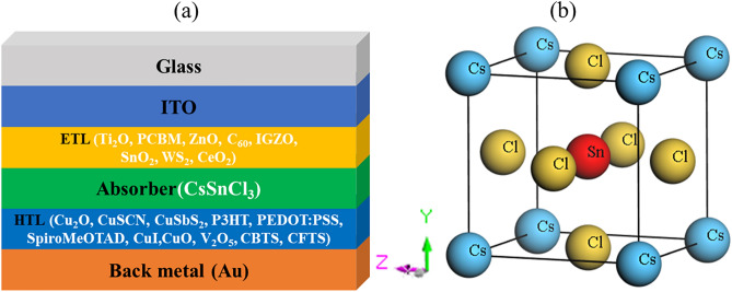
Tables 2 and 3 show the list of simulation parameters of the TCO, ETL, absorber, and HTL layers. Herein, SC architecture comprises indium-doped tin oxide (ITO) as the front contact, 8 ETLs, specified CsSnCl3 perovskite as an absorber, and 12 HTLs with gold (Au) as the back contact metal (Fig. 1a). Furthermore, the simulation parameters of interface defect density are outlined in Table 4. The simulation is run under the conditions of an AM1.5G simulated solar light exposure with a power density of 100 mW/cm2 at the ambient temperature (273 K). The only exception to this is the evaluation of the influence of working temperature on the efficiency of the device. During the initial simulation and further optimization, a standard absorption model with sqrt law (SCAPS traditional) was used.
Table 2.
| Parameters | ITO | TiO2 | PCBM | ZnO | C60 | IGZO | SnO2 | WS2 | CeO2 | CsSnCl3 |
|---|---|---|---|---|---|---|---|---|---|---|
| Thickness (nm) | 500 | 30 | 50 | 50 | 50 | 30 | 100 | 100 | 100 | 800* |
| Band gap, Eg (eV | 3.5 | 3.2 | 2 | 3.3 | 1.7 | 3.05 | 3.6 | 1.8 | 3.5 | 1.52 |
| Electron affinity, X (eV) | 4 | 4 | 3.9 | 4 | 3.9 | 4.16 | 4 | 3.95 | 4.6 | 3.90 |
| Dielectric permittivity (relative), εr | 9 | 9 | 3.9 | 9 | 4.2 | 10 | 9 | 13.6 | 9 | 29.4 |
| CB effective density of states, NC (1/cm3) | 2.2 × 10¹⁸ | 2 × 10¹⁸ | 2.5 × 10²¹ | 3.7 × 10¹⁸ | 8.0 × 10¹⁹ | 5 × 10¹⁸ | 2.2 × 10¹⁸ | 1 × 10¹⁸ | 1 × 10²⁰ | 1 × 10¹⁹ |
| VB effective density of states, NV (1/cm3) | 1.8 × 10¹⁹ | 1.8 × 10¹⁹ | 2.5 × 10²¹ | 1.8 × 10¹⁹ | 8.0 × 10¹⁹ | 5 × 10¹⁸ | 1.8 × 10¹⁹ | 2.4 × 10¹⁹ | 2 × 10²¹ | 1 × 10¹⁹ |
| Electron mobility, µn (cm2/Vs) | 20 | 20 | 0.2 | 100 | 8.0 × 10⁻² | 15 | 100 | 100 | 100 | 2 |
| Hole mobility, µh (cm2/Vs) | 10 | 10 | 0.2 | 25 | 3.5 × 10⁻³ | 0.1 | 25 | 100 | 25 | 2 |
| Shallow uniform acceptor density, NA (1/cm3) | 0 | 0 | 0 | 0 | 0 | 0 | 0 | 0 | 0 | 1 × 10¹⁵* |
| Shallow uniform donor density, ND (1/cm3) | 1 × 10²¹ | 9 × 10¹⁶ | 2.93 × 10¹⁷ | 1 × 10¹⁸ | 1 × 10¹⁷ | 1 × 10¹⁷ | 1 × 10¹⁷ | 1 × 10¹⁸ | 1021 | 0* |
| Defect density, Nt (1/cm3) | 1 × 10¹⁵* | 1 × 10¹⁵* | 1 × 10¹⁵* | 1 × 10¹⁵* | 1 × 10¹⁵* | 1 × 10¹⁵* | 1 × 10¹⁵* | 1 × 10¹⁵* | 1 × 10¹⁵* | 1 × 10¹⁵* |
*This study.
Table 3.
Input optimization parameters HTL the study56.
| HTL | Cu2O | CuSCN | CuSbS2 | P3HT | PEDOT: PSS | Spiro-MeOTAD | NiO | CuI | CuO | V2O5 | CFTS | CBTS |
|---|---|---|---|---|---|---|---|---|---|---|---|---|
| Thickness (nm) | 50 | 50 | 50 | 50 | 50 | 200 | 100 | 100 | 50 | 100 | 100 | 100 |
| Band gap, Eg (eV) | 2.2 | 3.6 | 1.58 | 1.7 | 1.6 | 3 | 3.8 | 3.1 | 1.51 | 2.20 | 1.3 | 1.9 |
| Electron affinity, Χ (eV) | 3.4 | 1.7 | 4.2 | 3.5 | 3.4 | 2.2 | 1.46 | 2.1 | 4.07 | 4.00 | 3.3 | 3.6 |
| Dielectric permittivity (relative), εr | 7.5 | 10 | 14.6 | 3 | 3 | 3 | 10.7 | 6.5 | 18.1 | 10.00 | 9 | 5.4 |
| CB effective density of states, NC (1/cm3) | 2 × 10¹⁹ | 2.2 × 10¹⁹ | 2 × 10¹⁸ | 2 × 10²¹ | 2.2 × 10¹⁸ | 2.2 × 10¹⁸ | 2.8 × 10¹⁹ | 2.8 × 10¹⁹ | 2.2 × 10¹⁹ | 9.2 × 10¹⁷ | 2.2 × 10¹⁸ | 2.2 × 10¹⁸ |
| VB effective density of states, NV (1/cm3) | 1 × 10¹⁹ | 1.8 × 10¹⁸ | 1 × 101 | 2 × 10²¹ | 1.8 × 10¹⁹ | 1.8 × 10¹⁹ | 1 × 10¹⁹ | 1 × 10¹⁹ | 5.5 × 10²⁰ | 5.0 × 10¹⁸ | 1.8 × 10¹⁹ | 1.8 × 10¹⁹ |
| Electron mobility, µn (cm2/Vs) | 200 | 100 | 49 | 1.8 × 10⁻³ | 4.5 × 10⁻² | 2.1 × 10⁻³ | 12 | 100 | 100 | 3.2 × 10² | 21.98 | 30 |
| Hole mobility, µh (cm2/Vs) | 8600 | 25 | 49 | 1.86 × 10⁻² | 4.5 × 10⁻² | 2.16 × 10⁻³ | 2.8 | 43.9 | 0.1 | 4.0 × 101 | 21.98 | 10 |
| Shallow uniform acceptor density, NA (1/cm3) | 1 × 10¹⁸ | 1 × 10¹⁸ | 1 × 10¹⁸ | 1 × 10¹⁸ | 1 × 10¹⁸ | 1.0 × 10¹⁸ | 1 × 10¹⁸ | 1.0 × 10¹⁸ | 1 × 10¹⁸ | 1 × 10¹⁸ | 1 × 10¹⁸ | 1 × 10¹⁸ |
| Shallow uniform donor density, ND (1/cm3) | 0 | 0 | 0 | 0 | 0 | 0 | 0 | 0 | 0 | 0 | 0 | 0 |
| Defect density, Nt (1/cm3) | 1.0 × 10¹⁵* | 1 × 10¹⁵* | 1 × 10¹⁵* | 1 × 10¹⁵* | 1 × 10¹⁵* | 1.0 × 10¹⁵* | 1 × 10¹⁵* | 1.0 × 10¹⁵* | 1 × 10¹⁵* | 1 × 10¹⁵* | 1 × 10¹⁵* | 1 × 10¹⁵* |
*In this study.
Figure 1.
(a) Design configuration of the CsSnCl3-based PSC, and (b) the optimized crystal structure of CsSnCl3 perovskite.
Table 4.
Input parameters of interface defect layers58.
| Interface | Defect type | Capture cross section: Electrons/holes (cm2) | Energetic distribution | Reference for defect energy level | Total density (cm−3) (integrated over all energies) |
|---|---|---|---|---|---|
| ETL/CsSnCl3 | Neutral |
1.0 × 10⁻¹⁷ 1.0 × 10⁻¹⁸ |
Single | Above the VB maximum | 1.0 × 10¹⁰ |
| CsSnCl3/HTL | Neutral |
1.0 × 10⁻¹⁸ 1.0 × 10⁻¹⁹ |
Single | Above the VB maximum | 1.0 × 10¹⁰ |
Results and discussions
Analysis of DFT results
Structural properties of CsSnCl3compound
The structural and phase stability of any material is a crucial criterion for the absorption of solar energy and applications in photovoltaic cells. The compound CsSnCl3 belongs to the cubic crystal family with the space group Pmm (No. 221). The crystallographic data of our studied SC absorber material is presented in Table 1. The Cs atom is at the eight corners, Cl atom is at the six faces, and the Sn atom is in the body-centered position with an SnCl6 octahedral structure in the unit cell of CsSnCl3 perovskite. Figure 1b illustrates the crystal structure of CsSnCl3 perovskite. The title compound contains five atoms in a unit cell, meaning that the unit cell has one formula unit. The crystal structure is optimized using the BFGS optimization technique to obtain minimum volume and energy data59. The estimated lattice parameters a = b = c = 5.629 Å and volume = 178.38 Å3 for the title perovskite compounds agree well with other experimental and theoretical data41,42 as shown in Table 1. The physical properties studied are expected to be reliable since the unit cell dimension mismatch is less than 1.0%. Furthermore, the optimized structure’s extremely low and negative formation energy value (ΔEf = − 1876.16 eV/atom) demonstrates its structural stability, which is compatible with solar system assembly.
Electronic band structure (BS) and density of states (DOS) of CsSnCl3 compound
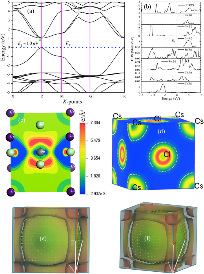
The electronic properties of CsSnCl3 halide lead-free Perovskite, are studied using a GGA within the framework of DFT as implemented in the CASTEP code51,60. The computed electronic properties such as band structure (BS) and density of states (DOS) are calculated along the highly symmetric X–R–M–G–R direction of the first Brillouin zone and are depicted in Fig. 2a,b, respectively. In Fig. 2a, the horizontal dotted line indicates the Fermi level (EF) and is set to zero (0). The energy band gap defined by the difference between the conduction and valence bands is estimated to be ~ 1.0 eV using the GGA functional. The calculated band gap (Eg) value is well justified with other reports using GGA/LDA functional42, but this value is much lower than some reported band gap values using non-local functional41,57. This underestimation of the band gap, especially for semiconductor materials using local functions like GGA and LDA, are widespread61,62. The strong Coulomb correlation and electron–electron interaction of the material might affect the band gap of the semiconductor63–65. However, it is seen from the band diagram that the material using local functional (GGA) is a direct bandgap semiconductor, which is found at the R point in the Brillouin zone. To observe the individual atomic contribution to the conductivity when external stimuli are applied and to acquire knowledge on band formation, we have also studied the total and partial DOS. The total and partial DOS for the CsSnCl3 compound is illustrated in Fig. 2b. It is seen that the valence band, which is very close to the Fermi level (EF), comprises Cl-3s orbital and Sn-5s/5p orbitals, while the nearest conduction band (very close to the EF) is composed of Sn-5p and Cl-3s orbitals. The prime contribution to the conductivity could come from the Sn element, as seen in Fig. 2b. The observed electronic contributions of constituent elements support the utilization of the CsSnCl3 compound as a solar absorber.
Figure 2.
The electronic (a) band structure and (b) DOS of halide perovskite, CsSnCl3, (c) and (d) The mapping images of electron density difference in the (110) and (001) planes for halide perovskite, CsSnCl3, (e) and (f)The Fermi surface topology of CsSnCl3 perovskite along (001) plane of two different orientations in the same Brillouin zone direction.
Electron charge density map of CsSnCl3 compound
The analysis of charge density distribution can reveal the type of chemical bonding that exists in the halide perovskite, CsSnCl3. The mapping image of the electron density difference in the (110) and (100) planes is depicted in Fig. 2c,d. Here, it is seen that maximum charge accumulation occurs around the Cl element for both planes, while its depletion is located around the Sn atom/element. In other words, the overlap of electron clouds between these two elements indicates covalent bonding63,65. This charge distribution channel strongly supports the covalent bonding nature that exists between Sn-Cl atoms. The charge distribution surrounding the atoms is observed to be nearly a sphere, which is a sign of ionic bonding and can be compared to previously reported perovskites66,67. Additionally, the Mulliken population analysis confirms that the Sn–Cl bond’s population value is positive and bigger than zero (0.37), demonstrating the bond's covalent character. On the other hand, the Sn–Cs and Cs–Cl bonds have a negative population value and are therefore determined to be an antibonding character.
Fermi surface topology of CsSsCl3 compound
The thermal, electrical, and optical properties of a compound can be described and predicted by its Fermi surface topology. Therefore, we also have studied the Fermi surface of the titled compound, which is presented in Fig. 2e,f. It is found that a spherical shape is located at the center (G-point) as a hole pocket. An open window is noticed at the six faces along the G-X direction for example. The eight open surfaces can be found at eight corners and are considered electron pockets. As a result, there are Fermi surfaces that resemble both electrons and holes, which suggests that the aforementioned material has multiple band features. Finally, it can be concluded that the highly dispersive band comprising the hybridization between Sn-5p and Cl-3s orbitals could be mainly responsible for the electronic conductivity.
Optical properties of CsSnCl3 compound
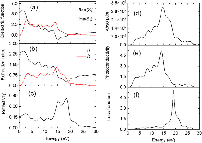
The photon energy-dependent dielectric function [real part, Ɛ1(ω) and imaginary part, Ɛ2(ω)] for CsSnCl3 has been studied in the energy range from 0 to 30 eV which is depicted in Fig. 3a. The corresponding formulas and theory can be found elsewhere68. The static value of the dielectric constant [Ɛ1(0)] can be estimated from the Penn model given in Eq. (11) 68.
| 11 |
where Ep, Eg, and EF indicate plasma energy, energy bandgap, and Fermi energy, respectively. The value of Ɛ1(0) signifies the index of refraction, which is very essential to fabricate many optoelectronic devices. The Ɛ1(0) value is noted to be 5.42. The highest value of Ɛ1(ω) is found to be ~ 6 at a photon energy of 1.57 eV and then gradually decreases to reach zero as well as negative values at 13.2 and 15 eV, respectively. After that, it is back to zero again at around 19.0 eV. This scenario of negative dielectric function in this frequency range is an indication of the Drude behavior of the compound. The absorption function of light can be expressed by the imaginary part of the energy-dependent dielectric function, Ɛ2(ω). The highest peak is noted at 3.6 eV and then a decreased tendency of light absorption is found with the increment of photon energy.
Figure 3.
Photon energy dependency of (a) dielectric function, (b) refractive index and (c) reflection coefficient; and (d) absorption coefficient, (e) photoconductivity and (f) loss function for halide perovskite, CsSnCl3 along (110) plane.
The energy-dependent refractive index (n) and extinction coefficient (k) are shown in Fig. 3b. It is well known that n governs light's speed relative to its free space in a compound, while k denotes its attenuation in a solid. The value of n(0) for CsSnCl3 is 2.26 eV. This value is almost constant (variation ~ 1.6%) in the IR and visible light energy region and then declines as light energy increases as shown in Fig. 3b. The greatest value of the refractive index was 2.28, and we can see that it declines with the increase of radiative light. The value of k follows an almost similar nature to that of Ɛ2(ω). The refractive index fluctuates with external frequency, indicating that CsSnCl3 has photorefractive characteristics.
The energy-dependent reflectance spectrum (R) is a crucial optical function for applying Kramers-Kroning relationships to calculate all optical coefficients. The reflectivity spectrum begins with ~ 16% reflectivity in this solar absorber material (Fig. 3c). The R-value (0. 16) at zero frequency is assumed to be the static component of reflectivity. It is seen from Fig. 3c that this spectrum is almost constant (variation ~ 2.9%) in the IR and visible light region (0–3.1 eV) and then broadly decreased in the near UV region owing to the inter-band transitions up to 6.7 eV. After that, some notable peaks are found at 8.43, 11.0, 15.27, and 18.57 eV and then again sharply decrease to reach zero value at ~ 30 eV of photon energy. The maximum reflectivity (0.41) is seen in the infrared range (3.85 eV) for the intra-band transitions in the compound, according to Fig. 3c.
The term absorption coefficient (α) offers crucial information about solar energy conversion efficiency by displaying the number of photons that a substance has absorbed. As shown in Fig. 3d, the absorption spectrum starts with a photon energy of ~ 1 eV, indicating that CsSnCl3 has an energy gap between the valence and conduction band (semiconducting nature). The absorption coefficient spectrum was increased with some prominent shoulder peaks at 5.66, 8.52, and 11.29 eV which suggests that the photon absorption initiates in the visible spectrum. The maximum value of the absorption coefficient was recorded at 14.84 eV. It is significant to note that with absorbed light, a semiconductor’s electrical conductivity and, consequently, photoconductivity, increase.
The photoconductivity of a material mainly depends on how much light energy is absorbed into the material. As shown in Fig. 3e, photoconductivity increases linearly in the visible light energy range, and then in the UV region, it rises with some distinct peaks at 3.3, 5.43, 8.36, and 11 eV. The maximum photoconductivity (4.8) is achieved when the incident photon energy is 14 eV. However, the photoconductivity typically decreases with photon energy after reaching its peak value.
The energy loss spectrum (L) of CsSnCl3 is depicted in Fig. 3f, which illustrates how much energy a fast electron loses while moving through a molecule. The energy loss of moving carriers is simply explained by the energy loss function. It is seen that energy loss slowly increased up to the light energy of 15.0 eV and then it increased rapidly. The highest energy loss could be obtained at around 19 eV, which is called plasma frequency (ωp). Because of the higher photon energy than Eg, it is evident that the majority of energy loss happens in the UV range.
Analysis of SCAPS-1D results
In this section, the PV performance of the ITO/ETL/CsSnCl3/HTL/Au structure is evaluated by keeping carrier concentration, thickness, and defect density of the ETL, absorber, and HTL layers constant along with 800 nm of CsSnCl3 absorber thickness, acceptor doping concentration of 1018 cm−3, and defect densities of 1015 cm−3 (Tables 2 and 3).
Effect of ETL
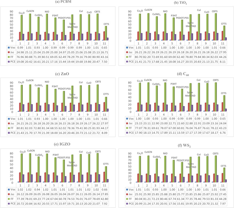
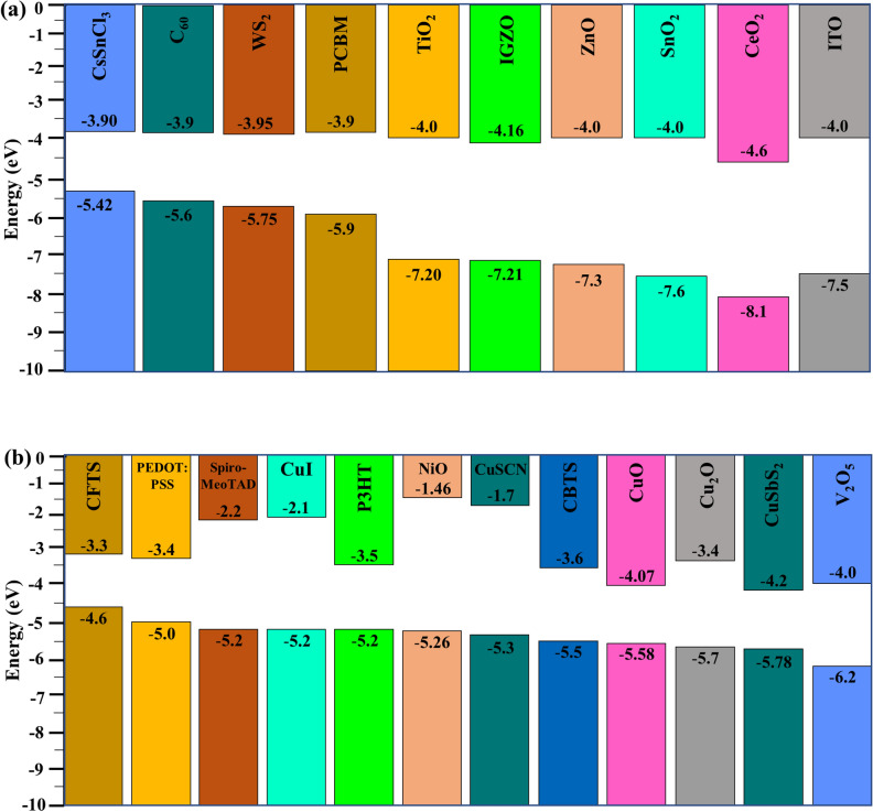
Figure 4 depicts that, the ETLs such as TiO2, ZnO, IGZO, WS2, PCBM, and C60 were inserted into the pristine heterostructure to obtain a configuration showing the highest photovoltaic performance. Our findings illustrate that ETLs of TiO2 and ZnO with a wide bandgap of 3.2 eV and 3.3 eV respectively and suitable electronic properties offer favorable transparency and band alignment (Figs. 5 and 6), which exhibited PCE of around 22% (Table 5), which is consistent with the previous report69. In contrast, ETLs like CeO2, PCBM, and C60 suffering from unsuitable bandgap and/or band alignment showed poor performance relatively. This finding shed light on the unsuitability of these candidates for SC configuration. Further, the optimum ETLs thickness of 30–50 nm, the donor concentration of 1017–1018 cm−3, and defect densities of 1015 cm−3 were obtained. The highest performance was found with the PCE of 21.75%, JSC of 26.22 mA/cm2, VOC of 1.01 V, and FF of 82.03% with ITO/TiO2/CsSnCl3/CBTS/Au heterostructure as shown in Table 5.
Figure 4.
Optimization of CsSnCl3 on PSC characteristics, i.e., VOC (V), JSC (mA/cm2), FF (%) and PCE (%) for various HTLs with Au as back metal contact and ETLs: (a) PCBM, (b) TiO2, (c) ZnO, (d) C60, (e) IGZO, and (f) WS2.
Figure 5.
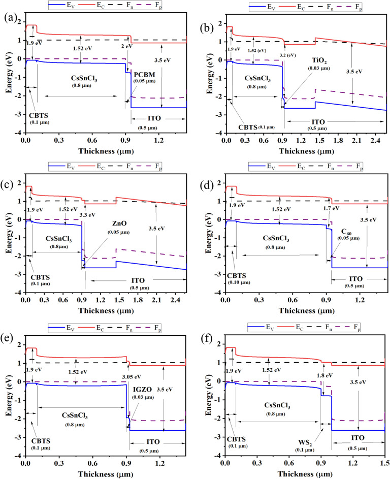
Band diagram of six optimized devices of CsSnCl3 with ETLs (a) C60, (b) IGZO, (c) PCBM, (d) TiO2, (e) WS2, (f) ZnO.
Figure 6.
Energy level alignment of the related (a) ITO, ETLs, and absorber CsSnCl3, and (b) HTLs.
Table 5.
Optimized performance parameters of the best combination for each of the ETLs and CBTS HTL.
| Optimized device | Cell thickness (μm) | Voc (V) | Jsc (mA/cm2) | FF (%) | PCE (%) |
|---|---|---|---|---|---|
| ITO/PCBM/CsSnCl3/CBTS | 0.5/0.05/0.8/0.1 | 1.01 | 25.13 | 80.9 | 20.47 |
| ITO/TiO2/CsSnCl3/CBTS | 0.5/0.03/0.8/0.1 | 1.01 | 26.22 | 82.03 | 21.75 |
| ITO/ZnO/CsSnCl3/CBTS | 0.5/0.05/0.8/0.1 | 1.01 | 26.22 | 81.93 | 21.72 |
| ITO/C60/CsSnCl3/CBTS | 0.5/0.05/0.8/0.1 | 1.00 | 23.16 | 78.22 | 18.17 |
| ITO/IGZO/CsSnCl3/CBTS | 0.5/0.03/0.8/0.1 | 1.02 | 26.14 | 78.69 | 21.07 |
| ITO/CeO2/CsSnCl3/CBTS | 0.5/0.1/0.8/0.1 | 0.85 | 26.06 | 65.37 | 14.43 |
| ITO/WS2/CsSnCl3/CBTS | 0.5/0.1/0.8/0.1 | 1.01 | 25.92 | 81.33 | 21.32 |
Effect of HTL
The HTLs such as CBTS, CuSCN, NiO, Cu2O, V2O5, and CFTS with more than twelve different combinations were studied (all are not shown here). The HTLs of CBTS offered much more favorable band alignment (Figs. 5 and 6), therefore, it exhibited the highest PCE around 22% for CsSnCl3 absorber-based SCs (Table 5). In contrast, the NiO, Cu2O, V2O5, and CFTS showed poor performance in comparison to others. So, there has been a dramatic improvement in performance while using the inorganic HTL. Since the HTL is made of inorganic materials that are more stable, transparent, and band-aligned, it has these advantages over organic HTL. Due to its distinct crystalline structure, light absorption, and atomic size, HTL CBTS, an earth-abundant material, performs well in each set of ETL29,37,38.
Band alignment of CsSnCl3-based heterostructure with different ETLs
Figures 5a–f show the band alignment of different CsSnCl3 absorber-based heterostructures with quasi-Fermi levels of electron and holes as Fn and Fp with conduction band minima and valence band maxima of EC and EV respectively. Fp is aligned with EV in each type of ETL, whereas Fn and EC continue harmonically. For TiO2 and ZnO ETLs, the bandgaps are nearly equal in comparison with the rest of the ETLs (Fig. 6), thereby, resulting in an almost equivalent performance with the same heterostructure. On the other hand, the Fp and EV remained at the same level for CBTS HTL and Fn cross through EC, which opposes holes entering from ETLs and electrons from HTL. Moreover, the rear contact Au collects holes from the HTL, whereas the front contact ITO collects electrons effectively. Herein, the gold was considered as the rear contact with a work function (WF) of 5.1 eV and indium dioxide with a WF of 4.0 eV acts as the front contact.
J-V and QE characteristics
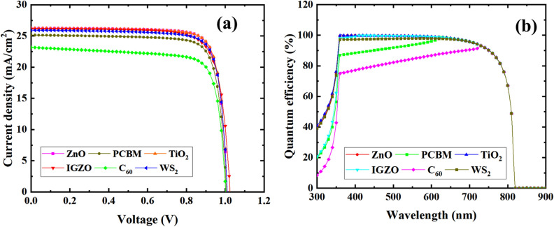
Figure 7 presents the J–V characteristics and QE for different ETLs for the device configuration of ITO/ETLs/CsSnCl3/CBTS/Au heterostructure. The QE computed in this manuscript is actually the external quantum efficiency (EQE). The maximum photocurrent was obtained in ITO/TiO2/CsSnCl3/CBTS/Au PSC while the minimum for ITO/C60/CsSnCl3/CBTS/Au (Fig. 7a). The favorable band alignment of TiO2 (Eg ~ 3.2 eV) ETL offers a higher current density while lower current in C60 (Eg ~ 2 eV) ETL owing to unsatisfactory band alignment. Thus, the ETLs band alignment influences the flow of photogenerated electrons or holes in CsSnCl3-based PSCs, which is consistent with previous reports57,70.
Figure 7.
Effect of (a) J–V, and (b) QE for six studied devices.
The corresponding QE as a function of wavelength (λ) was studied in the range of 300–900 nm as shown in Fig. 7b. This QE started to increase from 300 nm and dropped to 820 nm corresponding to the band edge of each active material. The QE was found maximum for ITO/TiO2/CsSnCl3/CBTS/Au heterostructure as expected from like J–V characteristics and the minimum for ITO/C60/CsSnCl3/CBTS/Au configuration. The higher band gap of TiO2 allows the higher photon to be absorbed in the CsSnCl3 absorber, resulting in the generation of higher current density. On the contrary, C60 with a smaller band gap (Eg ~ 2 eV) result in lower absorption in the absorber, therefore suppressing photocurrent. Thus, the band orientation of the ETLs affects significantly the light absorption, and consequently the photocurrent of cells71.
Effect of absorber and ETL thickness on cell performance
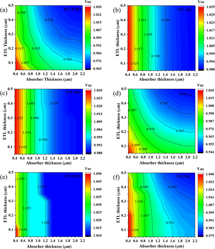
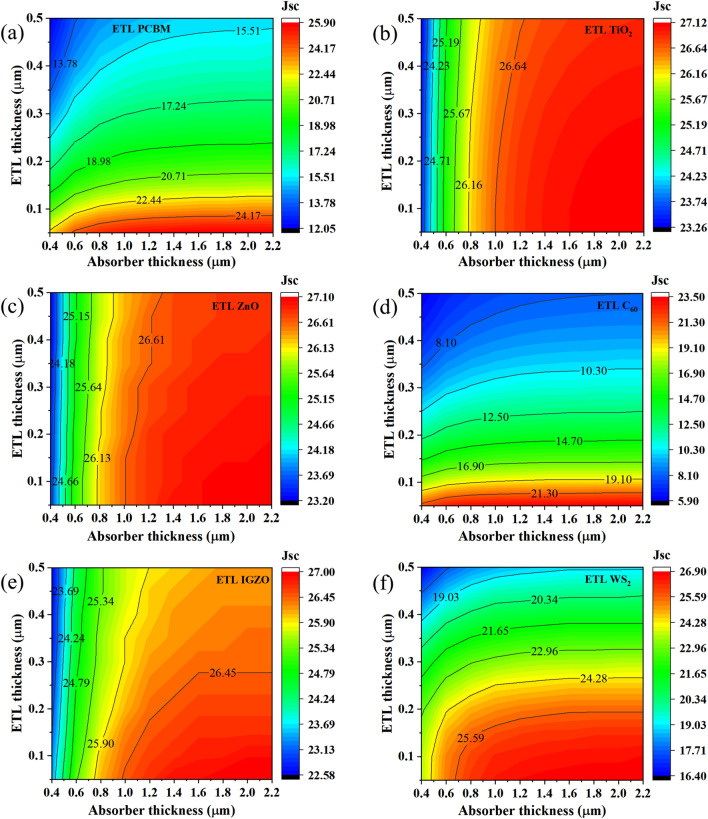
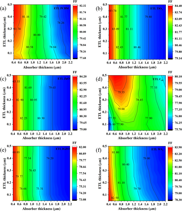
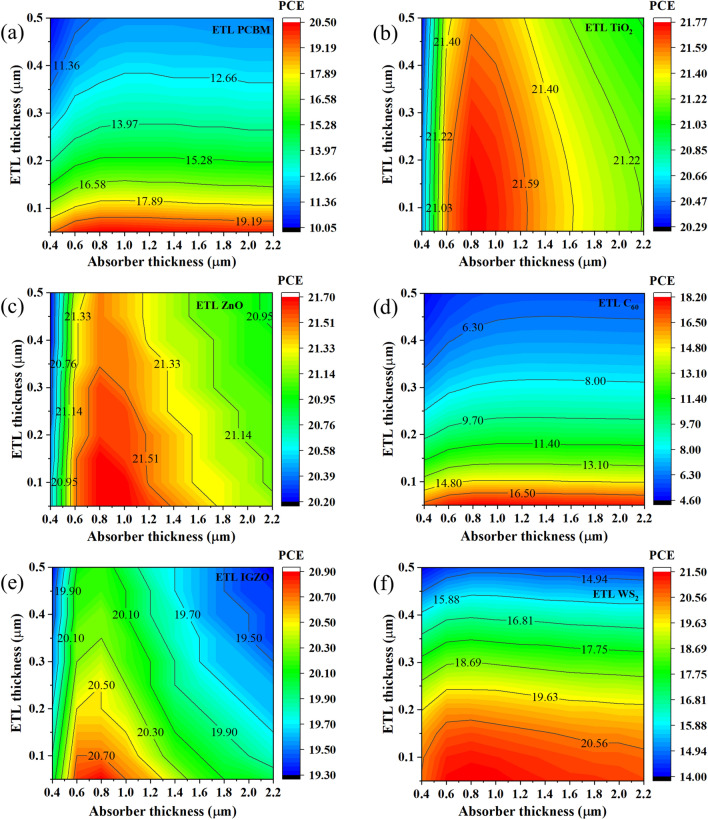
For the CsSnCl3-based PSCs, the contour maps of the computed VOC, JSC, FF, and efficiency with variable ETL thickness (50 nm to 500 nm) and absorber thickness (400 nm to 2200 nm) are depicted in Figs. 8, 9, 10 and 11. VOC was maximum at ~ 1.03–1.05 V for each device at an absorber thickness of 400 nm and at a varied ETL thickness from 50 to 100 nm. Among all devices, VOC was found to be a maximum of 1.050 V at a 400 nm-thick-CsSnCl3 absorber and 50 nm-thick IGZO ETL as depicted in Fig. 8e. And ETLs like PCBM, TiO2, and ZnO showed a slightly smaller VOC of 1.030 V at an absorber and ETL thickness of 400 nm and 100 nm respectively. Since the built-in potential formed by the six chosen ETLs is nearly equal as defined by their electron affinity value in the range of 3.9–4.1 eV, the VOC of each device shows almost the same value as ~ 1.03–1.05 V. The slight difference in terms of VOC between devices employing different ETL materials is mainly due to the bandgap difference. However, the VOC of all the devices tends to decrease with the increase of both absorber and ETL thickness over 500 and 50 nm respectively as observed in Fig. 8. This fact is due to the increased series resistance and reduced photocurrent.
Figure 8.
Contour mapping of VOC for CsSnCl3 absorber and ETLs (a C60, b IGZO, c PCBM, d TiO2, e WS2, and f ZnO) thickness.
Figure 9.
Contour mapping of JSC for CsSnCl3 absorber thickness and ETLs (a C60, b IGZO, c PCBM, d TiO2, e WS2, and f ZnO) thickness.
Figure 10.
Contour mapping of FF for CsSnCl3 absorber thickness and ETLs (a C60, b IGZO, c PCBM, d TiO2, e WS2, and f ZnO) thickness.
Figure 11.
Contour mapping of PCE for CsSnCl3 absorber thickness and ETLs (a C60, b IGZO, c PCBM, d TiO2, e WS2, and f ZnO) thickness.
Figure 9 illustrates the JSC for different ETL configurations whereas the highest JSC was observed in the range of ~ 23.50–27.12 mA/cm2 at an absorber thickness of ≥ 800 nm and ETL thickness of 50–100 nm. The highest JSC of 27.12 mA/cm2 was obtained by TiO2 ETL with absorber thickness of ≥ 1400 nm and ETL thickness of 150 nm for each of the six studied heterostructures. On the contrary, a smaller JSC of 23.50 mA/cm2 was obtained by C60 ETL with an absorber thickness of ≥ 1400 nm and ETL thickness of 50 nm. The relatively higher JSC observed in TiO2, ZnO, and IGZO ETLs-based heterostructure owing to their wide band gap and good light penetration depth through these materials, resulting in, the allowance of the higher amount of incident light to be absorbed in the absorber layer. In addition, higher absorber thickness confirms the absorption of higher wavelength light spectra, resulting in an improved JSC. However, the JSC of all devices starts to decrease for absorber thickness of ≥ 1000 nm and ETL thickness of ≥ 100 nm because of the domination of recombination at thicker device structure than carrier lifetime.
Figure 10 shows the FF for different ETLs configurations, where the highest FF was observed in the range of ~ 80.1–84.4% corresponding to the absorber and ETL thickness of 400–600 nm and 400–500 nm respectively for the investigated heterostructures. Maximum FF of 84.4% was obtained for TiO2 ETL with absorber and ETL thickness of 400 and 450 nm respectively and the FF was relatively smaller at 80.1% for C60 ETL with the absorber and ETL thickness of 600 nm and 450 nm respectively. So far, the FF decreased at an absorber thickness of ≥ 600 nm and ETL thickness of ≤ 400 nm for every heterostructure, owing to the absorber thickness being greater than the diffusion length, thereby generating noticeable recombination of photogenerated charrier in the quasi-neutral region. Besides, reduced ETL thickness will increase the film resistivity which hinders the FF. Otherwise, a strong electric field developed across the absorber layer originates from the FF, and an increasing absorber thickness causes a weakening of the overall electric field’s strength and thereby formation of a quasi-neutral region in the absorber layer. Besides, the formation of a quasi-neutral layer causes the carriers to transport through diffusion rather than drift, which led to a reduction of FF with increasing series resistance.
As a result, the highest efficiency in the range of ~ 18.20–21.77% was obtained for all studied heterostructures at an ETL thickness of 50–100 nm, and absorber thickness of 800–1200 nm (Fig. 11). As expected from the aforementioned VOC, JSC and FF results, the efficiency of 21.77% was the highest for TiO2 ETL with the absorber and ETL thickness of 800 and 50 nm accordingly. The efficiency of ETL C60 was found relatively smaller at 18.20% with absorber and ETL thickness of 1200 and 50 nm respectively. Therefore, the optimum absorber and ETL thickness of 800–1200 and 50–100 nm was obtained for chosen six different ETL configurations. However, the ETLs of TiO2, ZnO, and IGZO-with CsSnCl3 absorber-based heterostructures were found much more efficient and promising than the rest of the structures. These simulated results are consistent with the previous report72.
The effect of ETL thickness variation on the PV parameters, i.e., PCE, FF, JSC, and VOC is shown in Fig. S1. It is clearly seen that the increase in the thickness of the ETL leads to the degradation in the PV parameters for most of the ETLs, thereby leading to a decrement in PCE. This is due to the inefficient transport of charge carriers to the electrodes, the increase in series resistance that degrades the FF, and the increase in the probability of recombination with increasing ETL thickness73.
Effect of series resistance
There are three factors that contribute to series resistance in solar cells: first, the flow of current via the SC’s ETL/PVK and PVK/HTL interfaces (here PVK means “Perovskite”); second, the metal contact/ITO interface resistance; and third, the resistance of the top and rear metal contacts. Series resistance mostly affects the FF reduction, while extremely high values may also have a negative effect on short-circuit current.
Several experimental procedures may be used to control or minimize series resistance. For instance, an ETL film created by thermal oxidation is extremely dense and suppresses recombination at the ETL/PVK interface, thereby lowering series resistance74. The ETL film made by thermal oxidation has a thinner ideal thickness compared to the one made by spin-coating, which lowers the series resistance. Additionally, compared to two-step sintering, one-step sintering results in reduced dark current densities, reduced series resistance, and stronger recombination resistance75. Additionally, perovskite films were molecularly doped to increase their conductivity and electronic contact with the conductive substrate, which decreased their series resistance76.
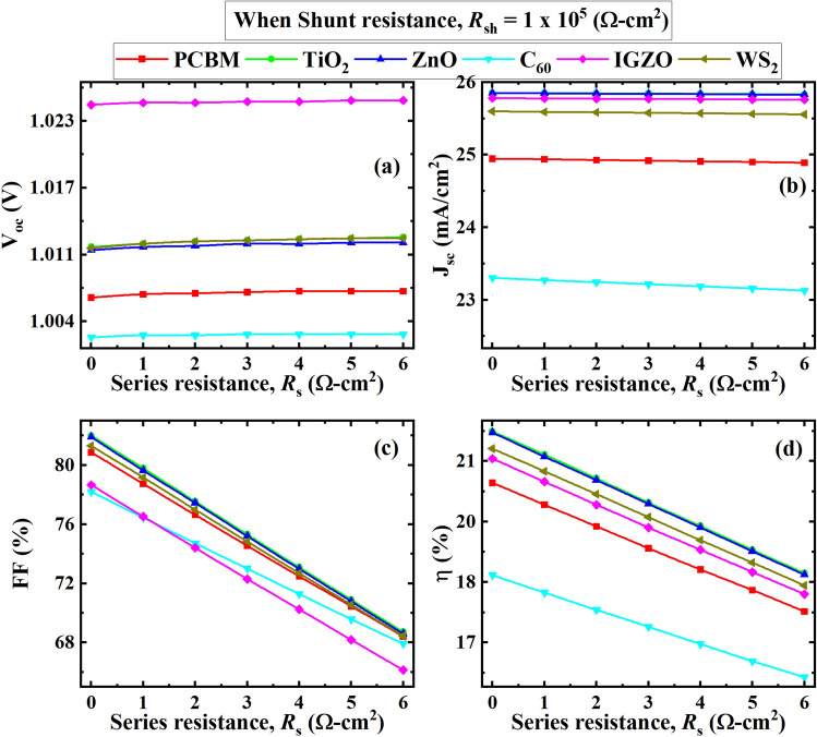
Figure 12 illustrates the impact of series resistance (RS) on the PSC performance in the ranges of 0 to 6 Ω cm2, at a constant shunt resistance (RSH) of 105 Ω cm2. The FF was found as the most affected parameter for the varied RS than VOC, and JSC.
Figure 12.
Effect of RS on (a) VOC; (b) JSC; (c) FF; (d) PCE at an RSH = 105 Ω cm2.
In Fig. 12, the FF decreased drastically from 84.5 to 66% with an increase in RS from 0 to 6 Ω cm2 while the VOC and JSC were affected insignificantly in every device. The IGZO/CsSnCl3/CBTS and TiO2/CsSnCl3/CBTS PSC structures showed the highest VOC and JSC respectively whereas C60/CsSnCl3/CBTS PSC structure showed relatively poor performance. Higher RS affects FF significantly, thereby the conversion efficiency in the PSCs with different heterostructures. Equations (12) and (13) illustrate the effect of RS on solar cell parameters, especially short circuit current ISC.
| 12 |
| 13 |
where IL denotes light-induced current and denotes shunt resistance. It is obvious from the formula above as RS increases, the ISC value drops. The decrease in efficiency and FF is primarily due to this77,78.
Effect of shunt resistance
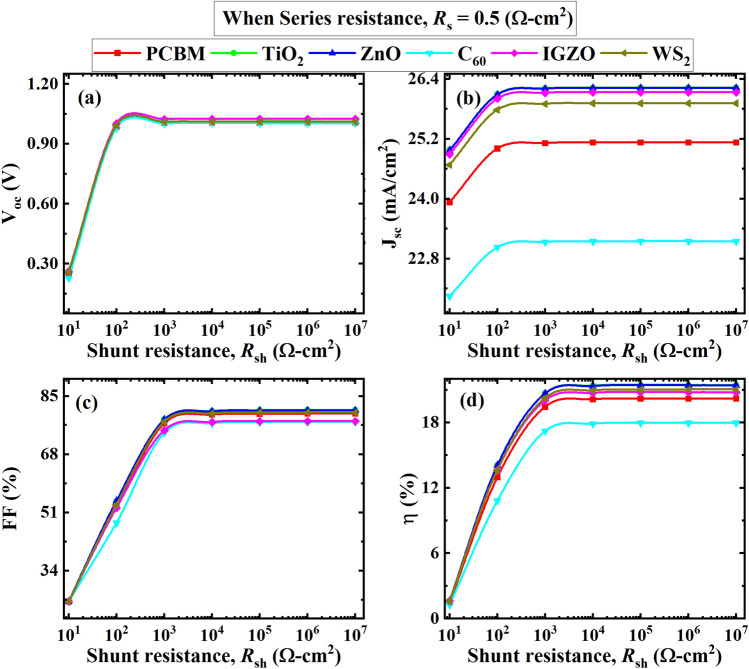
Leakage current and non-geminated recombination losses are responsible for the considerable power losses brought on by the existence of a shunt resistance in PSCs. Due to the creation of pinholes and the metal filling of these pinholes extending to the junctions, there are occasional partial shorts of the junctions in practical solar cells. Low shunt resistance results in power losses in solar cells by giving the current produced by light an alternative path. A similar diversion lowers the voltage generated by the solar cell and lowers the current passing through the junction of the SC. Since there would be a lower light-generated current at low light levels, the influence of shunt resistance is more severe. Accordingly, the effect of losing this current to the shunt is higher. Additionally, the influence of resistance in parallel is significant at lower voltages when the effective resistance of the SC is considerable. Various techniques are used to control or reduce shunt resistance. For instance, a simple way for improving SnO2’s electron transport layer (ETL) involves doping the precursor nanoparticles with modest quantities of a Pb source, which effectively raises the shunt resistance. So, adjusting the Pb quantity makes it simple to alter the Rsh value79.
Figure 13 shows the effect of RSH in the ranges of 10–107 Ω cm2 with ITO/ETL/CsSnCl3/CBTS/Au heterostructure at a constant RS of 0.5 Ω cm2. The figure illustrates the significant variation of PV parameters VOC, JSC, FF, and PCE at a varied shunt resistance. Herein, the PV parameters of VOC, JSC, FF, and consequently PCE increase markedly from 2 to ~ 23% when RSH increases from 10 to 103 Ω cm2. The PCE reached the highest value of ~ 22% at RSH of 104 and remained constant up to 107 Ω cm2 or beyond RSH. The primary origin of RSH is the defects formed during the manufacturing process. The structure becomes a low-resistance path for current flow at a higher RSH value56,80. Herein, the VOC increased with shunt resistance up to 8000 Ω cm2 while the JSC was found almost constant as observed in the previous investigation81. Thus, a high value of of ≥ 104 is favorable to obtain the highest PCE in ITO/ETL/CsSnCl3/CBTS/Au PSCs.
Figure 13.
Effect of RSH on (a) VOC; (b) JSC; (c) FF; (d) PCE at an RS = 0.5 Ω cm2.
Effect of temperature
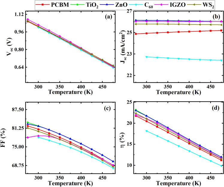
Figure 14 shows the impact of temperature changes on the performance benchmarks for the six devices, including VOC, JSC, FF, and PCE corresponding to working temperature from 275 to 475 K for an ITO/ETL/CsSnCl3/CBTS/Au heterojunction PSC under 1000 Wm−2 solar light.
Figure 14.
Effect of the variation in temperature from 275 to 475 K on (a) VOC; (b) JSC; (c) FF; and (d) PCE.
For classical semiconductors, the relationship between temperature and solar cell characteristics is well described82. From Fig. 14, the characteristic mainly affected by temperature rise in traditional solar cells is VOC, which falls with temperature increase, owing to a continuous increase in the saturation current with temperature83. The shift in intrinsic carrier concentrations that occurs when the temperature rises cause higher rates of recombination, which in turn has a major impact on the saturation current83.
The reliance of JSC for PSCs may be roughly described as a linear connection, the same as how it is for VOC84. The JSC in an SC is often defined as the product of the ideal current and the collecting fraction. The ideal current is the current that might be created if most incident photons with energies greater than the bandgap were absorbed without losses, whereas the collection fraction is a consequence of charge carrier reflection, transmission, parasitic absorption, and recombination in the SC. From Fig. 14, the variations in JSC with temperature are significantly lower than the changes in VOC. Notwithstanding the commonly approved linear dependence of JSC on the temperature in conventional SCs, it is unclear how the JSC shifts with temperature in PSCs because increasing the bandgap causes a decrease in the ideal current while the collection fraction rises typically with temperature85. As a result, depending on which of these factors predominate, the JSC may drop or rise with temperature.
Effect of capacitance and Mott-Schottky
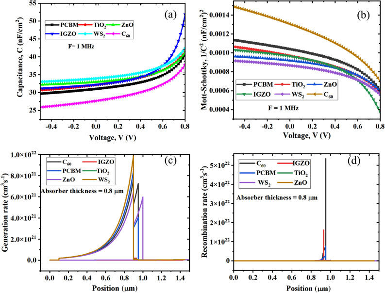
The influence of capacitance and Mott-Schottky versus a voltage range of − 0.5 V to 0.8 V with a fixed frequency of 1 MHz for six different configurations of CsSnCl3-based PSCs with different ETLs, is shown in Fig. 15a,b respectively. In Fig. 15a, the capacitance increases exponentially with an increase in supply voltage and reaches saturation. The highest amount of capacitance of 52.5 C was observed for IGZO ETL-based device, whereas the lowest capacitance for C60 ETL at 0.8 V. At zero bias, the device is in depletion condition; however, when a forward bias of around 0.5 V is applied, the depletion width falls to a value that is almost equal to the thickness of the absorber layer. As a result, the capacitance rises for further applied forward bias voltage retaining a consistent Mott-Schottky relationship. The current is only allowed to surpass the contact's saturation current during voltage spikes, contrary to what has previously been seen, where it is considerably reduced during low voltages.
Figure 15.
(a) The capacitance–voltage (C–V) response, (b) Mott-Schottky (1/C2) response, (c) generation rate, (d) recombination rate for absorber CsSnCl3-based heterostructures with six different ETLs.
The built-in potential (Vbi), which distinguishes between the activities of electrode operation and doping level, can be calculated with the help of the widely used Mott-Schottky (MS) method. The intercept point on the x-axis of the C–V curve typically corresponds to the Vbi of the respective junction and the intercept point of the 1/C2–V curve denotes the concentration of occupied trapping centers. With an increase in Vbi values, the MS values fall for a particular device. Herein, the simulated results obtained at an identical condition of all of the significant criteria for each of the devices were comparable and consistent with earlier reports70.
Effect of generation and recombination rate
The carrier generation and recombination rates for CsSnCl3-based PSCs are shown in Fig. 15c,d at a range of 0.0–1.5 μm. When an electron is stimulated from the valence band to the conduction band due to the absorption of a photon, a hole is created in the valence band, and this process produces electron–hole pairs. According to the findings, all the device generation rates peak between 0.9 and 1.0 μm. SCAPS-1D calculates the formation of electron–hole pairs G(x) using the arriving photon flux Nphot (λ, x), and Eq. (14) analyses this photon flux to show the value of G(x) for every spectrum and location.
| 14 |
On the other hand, the recombination rate is exactly opposite to the generation process, which unites and eliminates the generated electrons and holes. The rate of recombination in PSCs is influenced by the charge carrier's lifetime and density. The decrease in electron–hole recombination is caused by the defect states that exist within the absorber layer. The maximum recombination rate was observed between 0.9 and 1.0 μm for all studied devices while C60 ETL contained the highest recombination peak. The energy levels generated mid-level of the valence-conduction band cause electron–hole recombination within the devices noticeably. The PSCs’ recombination rate distribution can be non-uniform due to grain boundaries and device manufacturing flaws56,80.
Comparison with wxAMPS results and previous work
Comparison between SCAPS-1D and wxAMPS results
The simulations were further conducted by the wxAMPS (version 2.0) program to validate the obtained results (Table 6) by SCAPS-1D at a working temperature of 300 K and using an AM1.5G solar spectrum. Both software programs ran simulations using absorber thickness, absorber acceptor concentrations, and defect concentrations of 800 nm, 1015 cm-3, and 1015 cm−3, respectively to determine how the PV properties of all the CsSnCl3 devices are affected. Table 6 presents a comparison of software simulations using SCAPS-1D and wxAMPS. The closeness between the two simulation results (especially FF and Voc) obtained by wxAMPS and SCAPS-1D revealed the validation of obtained results, which are also inconsistent with earlier studies56,80.
Table 6.
Comparison between SCAPS-1D and wxAMPS software simulation results for CsSnCl3 PSCs.
| Device structure | Software | Voc (V) | Jsc (mA/cm2) | FF (%) | PCE (%) |
|---|---|---|---|---|---|
| ITO/PCBM/CsSnCl3/CBTS/Au | SCAPS-1D | 1.01 | 25.13 | 80.90 | 20.47 |
| wxAMPS | 0.99 | 16.79 | 80.92 | 13.52 | |
| ITO/TiO2/CsSnCl3/CBTS/Au | SCAPS-1D | 1.01 | 26.22 | 82.03 | 21.75 |
| wxAMPS | 1.01 | 21.25 | 82.23 | 17.68 | |
| ITO/ZnO/CsSnCl3/CBTS/Au | SCAPS-1D | 1.01 | 26.22 | 81.93 | 21.72 |
| wxAMPS | 1.00 | 20.26 | 80.83 | 16.46 | |
| ITO/C60/CsSnCl3/CBTS/Au | SCAPS-1D | 1.00 | 23.16 | 78.22 | 18.17 |
| wxAMPS | 0.99 | 17.15 | 80.94 | 13.84 | |
| ITO/IGZO/CsSnCl3/CBTS/Au | SCAPS-1D | 1.02 | 26.14 | 78.69 | 21.07 |
| wxAMPS | 1.02 | 21.51 | 79.84 | 17.47 | |
| ITO/WS2/CsSnCl3/CBTS/Au | SCAPS-1D | 1.01 | 25.92 | 81.33 | 21.32 |
| wxAMPS | 1.01 | 21.02 | 80.93 | 17.13 |
Comparison of SCAPS-1D results with previous work
Table 7 compares our obtained outcomes to recent experimental and theoretical findings of CsSnCl3-based PSCs for a different configuration. The highest experimental PCE of 17.93% is reported FTO/PCBM/CsSnCl3/PTAA/Au heterostructure. To date, the theoretical research conducted for improving the performance of the CsSnCl3 absorber, and the highest PCE of < 20.0% was found through simulation. Herein, we have reported the maximum PCE of ~ 22.0% for the very first time. Further, we conducted an extensive simulation for finding an effective ETL, HTL, back metal contact, and so on. However, we conducted all of these simulations to identify the ideal pairings for a stellar performance. In addition, experimental work is in demand for the time to validate the theoretical study that will conduct in near future.
Table 7.
The comparison of PV parameters of CsSnCl3-based solar cells.
| Device structure | Absorber thickness (μm) | Voc (V) | Jsc (mA/cm2) | FF (%) | PCE (%) | Ref |
|---|---|---|---|---|---|---|
| FTO/PCBM/CsSnCl3/PTAA/Au | 1.0 | 1.30 | 15.34 | 89.90 | 17.93 | 57 |
| ITO/PCBM/CsSnCl3/CBTS/Au | 0.8 | 1.01 | 25.13 | 80.9 | 20.47 | * |
| ITO/TiO2/CsSnCl3/CBTS/Au | 0.8 | 1.01 | 26.22 | 82.03 | 21.75 | * |
| ITO/ZnO/CsSnCl3/CBTS/Au | 0.8 | 1.01 | 26.22 | 81.93 | 21.72 | * |
| ITO/C60/CsSnCl3/CBTS/Au | 0.8 | 1.00 | 23.16 | 78.22 | 18.17 | * |
| ITO/IGZO/CsSnCl3/CBTS/Au | 0.8 | 1.02 | 26.14 | 78.69 | 21.07 | * |
| ITO/WS2/CsSnCl3/CBTS/Au | 0.8 | 1.01 | 25.92 | 81.33 | 21.32 | * |
*This work.
Conclusion
A detailed numerical study on CsSnCl3 absorber-based Pb-free SCs from 96 configurations has been performed using the SCAPS-1D simulator. Utilizing the most efficient six device configurations among 96 heterostructures, we further investigated the effects of the CsSnCl3 and ETL thickness, series and shunt resistance, and operating temperature. Further, the effects of C–V characteristics like capacitance, and Mott-Schottky, along with generation and recombination rates, J–V characteristics, and quantum efficiency were also assessed. The TiO2 ETL and CBTS HTL-based heterojunction with ITO/TiO2/CsSnCl3/CBTS/Au device configuration showed the highest PCE of 21.75% with VOC of 1.01 V, JSC of 26.22 mA/cm2, and FF of 82.03% from six optimized devices. Meanwhile, the ZnO, WS2, IGZO, PCBM, and C60-based devices showed PCE of 21.72, 21.32, 21.07, 20.47, and 18.17% respectively. Furthermore, these simulated results obtained by SCAPS-1D were reproduced and validated using wxAMPS numerical study. Moreover, first-principles DFT simulations with the CASTEP program were performed to investigate the structural, electrical, and optical characteristics of the CsSnCl3 absorber. The calculated band gap for the CsSnCl3 absorber was 1.0 eV and the Sn-5s/5p orbital electrons displayed significant hybridization based on the estimated partial DOS. The charge density difference analysis strongly supports the covalent bonding nature between Sn-Cl atoms. The observed Fermi surface exhibits hole and electron-like pockets, demonstrating the multiband character of the CsSnCl3 perovskite. Thus, these extensive simulations with validation results revealed the high potential of CsSnCl3 absorber with TiO2, ZnO, IGZO, WS2, PCBM, and C60 ETLs and CBTS HTL, thereby paving a constructive research avenue for the photovoltaic industry to fabricate cost-effective, high-efficiency, and lead-free CsSnCl3-based solar cells. Our future perspective is to use combined DFT-SCAPS-Machine Learning technique to critically investigate nontoxic perovskite devices (ABX3: A = Cs; B = Sn, Bi, Ge, Ag, and Sb and X = I, Br) employing competitive charge transport materials, thereby offering researchers a clear guidance towards enhancing PCE values.
Supplementary Information
Acknowledgements
The SCAPS-1D program was provided by Dr. M. Burgelman of the University of Gent in Belgium. The authors would like to express their gratitude to him. They would also like to thank Professor A. Rockett and Dr. Yiming Liu from UIUC, as well as Professor Fonash from Penn State University, for their contributions to the wxAMPS program.
Author contributions
M.K.H.: Conceptualization, Methodology, Software, Validation, Formal analysis, Investigation, Data curation, Writing—original draft, Writing—review and editing, Supervision, Project administration; G.F.I.T.: Formal analysis, Investigation, Data curation, Writing—original draft; A.K.: Writing—review and editing; M.H.K.R.: Software, Data curation; Formal analysis, Investigation, Writing—review and editing; M.M.H., H.B., M.F.R., M.R.I., and M.M.: Validation, Formal analysis, Writing—review and editing.
Data availability
The datasets used and/or analysed during the current study available from the corresponding author on reasonable request.
Competing interests
The authors declare no competing interests.
Footnotes
Publisher's note
Springer Nature remains neutral with regard to jurisdictional claims in published maps and institutional affiliations.
Contributor Information
M. Khalid Hossain, Email: khalid.baec@gmail.com, Email: khalid@kyudai.jp.
M. H. K. Rubel, Email: mhk_mse@ru.ac.bd
Supplementary Information
The online version contains supplementary material available at 10.1038/s41598-023-28506-2.
References
- 1.Palazon F, et al. Polymer-free films of inorganic halide perovskite nanocrystals as UV-to-white color-conversion layers in LEDs. Chem. Mater. 2016;28:2902–2906. doi: 10.1021/acs.chemmater.6b00954. [DOI] [PMC free article] [PubMed] [Google Scholar]
- 2.Wang Y, Wan J, Ding J, Hu J, Wang D. A rutile tio2electron transport layer for the enhancement of charge collection for efficient perovskite solar cells. Angew. Chem. Int. Ed. 2019;58:9414–9418. doi: 10.1002/anie.201902984. [DOI] [PubMed] [Google Scholar]
- 3.Saparov B, et al. Thin-film deposition and characterization of a Sn-deficient perovskite derivative Cs2SnI6. Chem. Mater. 2016;28:2315–2322. doi: 10.1021/acs.chemmater.6b00433. [DOI] [Google Scholar]
- 4.Lee B, et al. Air-stable molecular semiconducting iodosalts for solar cell applications: Cs2SnI6 as a hole conductor. J. Am. Chem. Soc. 2014;136:15379–15385. doi: 10.1021/ja508464w. [DOI] [PubMed] [Google Scholar]
- 5.Qiu X, et al. From unstable CsSnI3 to air-stable Cs2SnI6: A lead-free perovskite solar cell light absorber with bandgap of 1.48 eV and high absorption coefficient. Sol. Energy Mater. Sol. Cells. 2017;159:227–234. doi: 10.1016/j.solmat.2016.09.022. [DOI] [Google Scholar]
- 6.Qiu X, et al. Lead-free mesoscopic Cs2SnI6 perovskite solar cells using different nanostructured ZnO nanorods as electron transport layers. Phys. Status Solidi Rapid Res. Lett. 2016;10:587–591. doi: 10.1002/pssr.201600166. [DOI] [Google Scholar]
- 7.Bencherif H, Hossain MK. Design and numerical investigation of efficient (FAPbI3)1–x(CsSnI3)x perovskite solar cell with optimized performances. Sol. Energy. 2022;248:137–148. doi: 10.1016/j.solener.2022.11.012. [DOI] [Google Scholar]
- 8.Yin W-J, Shi T, Yan Y. Unique properties of halide perovskites as possible origins of the superior solar cell performance. Adv. Mater. 2014;26:4653–4658. doi: 10.1002/adma.201306281. [DOI] [PubMed] [Google Scholar]
- 9.Miyata A, et al. Direct measurement of the exciton binding energy and effective masses for charge carriers in organic–inorganic tri-halide perovskites. Nat. Phys. 2015;11:582–587. doi: 10.1038/nphys3357. [DOI] [Google Scholar]
- 10.Bencherif H, et al. Performance enhancement of (FAPbI3)1–x(MAPbBr 3)x perovskite solar cell with an optimized design. Micro Nanostruct. 2022;171:207403. doi: 10.1016/j.micrna.2022.207403. [DOI] [Google Scholar]
- 11.Shao Y, et al. Grain boundary dominated ion migration in polycrystalline organic–inorganic halide perovskite films. Energy Environ. Sci. 2016;9:1752–1759. doi: 10.1039/C6EE00413J. [DOI] [Google Scholar]
- 12.Rolston N, et al. Engineering stress in perovskite solar cells to improve stability. Adv. Energy Mater. 2018;8:1802139. doi: 10.1002/aenm.201802139. [DOI] [Google Scholar]
- 13.Wu W-Q, et al. Bilateral alkylamine for suppressing charge recombination and improving stability in blade-coated perovskite solar cells. Sci. Adv. 2019;5:eaav8925. doi: 10.1126/sciadv.aav8925. [DOI] [PMC free article] [PubMed] [Google Scholar]
- 14.Hossain MK, et al. Influence of natural dye adsorption on the structural, morphological and optical properties of TiO2 based photoanode of dye-sensitized solar cell. Mater. Sci. 2017;36:93–101. [Google Scholar]
- 15.Hossain MK, et al. A comparative study on the influence of pure anatase and Degussa-P25 TiO2 nanomaterials on the structural and optical properties of dye sensitized solar cell (DSSC) photoanode. Optik (Stuttg) 2018;171:507–516. doi: 10.1016/j.ijleo.2018.05.032. [DOI] [Google Scholar]
- 16.Hossain MK, et al. Annealing temperature effect on structural, morphological and optical parameters of mesoporous TiO2 film photoanode for dye-sensitized solar cell application. Mater. Sci. 2017;35:868–877. [Google Scholar]
- 17.Mia MNH, et al. Influence of Mg content on tailoring optical bandgap of Mg-doped ZnO thin film prepared by sol-gel method. Results Phys. 2017;7:2683–2691. doi: 10.1016/j.rinp.2017.07.047. [DOI] [Google Scholar]
- 18.Pervez MF, et al. Influence of total absorbed dose of gamma radiation on optical bandgap and structural properties of Mg-doped zinc oxide. Optik (Stuttg) 2018;162:140–150. doi: 10.1016/j.ijleo.2018.02.063. [DOI] [Google Scholar]
- 19.Kim H-S, et al. Lead Iodide perovskite sensitized all-solid-state submicron thin film mesoscopic solar cell with efficiency exceeding 9% Sci. Rep. 2012;2:591. doi: 10.1038/srep00591. [DOI] [PMC free article] [PubMed] [Google Scholar]
- 20.Lee MM, Teuscher J, Miyasaka T, Murakami TN, Snaith HJ. Efficient hybrid solar cells based on meso-superstructured organometal halide perovskites. Science. 2012;338:643–647. doi: 10.1126/science.1228604. [DOI] [PubMed] [Google Scholar]
- 21.Mei A, et al. A hole-conductor-free, fully printable mesoscopic perovskite solar cell with high stability. Science. 2014;345:295–298. doi: 10.1126/science.1254763. [DOI] [PubMed] [Google Scholar]
- 22.Yu J-G, et al. The effect of calcination temperature on the surface microstructure and photocatalytic activity of TiO2 thin films prepared by liquid phase deposition. J. Phys. Chem. B. 2003;107:13871–13879. doi: 10.1021/jp036158y. [DOI] [Google Scholar]
- 23.Diao X-F, et al. Study on the property of electron-transport layer in the doped formamidinium lead iodide perovskite based on DFT. ACS Omega. 2019;4:20024–20035. doi: 10.1021/acsomega.9b03015. [DOI] [PMC free article] [PubMed] [Google Scholar]
- 24.Baktash A, Amiri O, Sasani A. Improve efficiency of perovskite solar cells by using Magnesium doped ZnO and TiO2 compact layers. Superlattices Microstruct. 2016;93:128–137. doi: 10.1016/j.spmi.2016.01.026. [DOI] [Google Scholar]
- 25.Kavan L. Conduction band engineering in semiconducting oxides (TiO2, SnO2): Applications in perovskite photovoltaics and beyond. Catal. Today. 2019;328:50–56. doi: 10.1016/j.cattod.2018.10.065. [DOI] [Google Scholar]
- 26.Kim IS, et al. Amorphous TiO2 compact layers via ALD for planar halide perovskite photovoltaics. ACS Appl. Mater. Interfaces. 2016;8:24310–24314. doi: 10.1021/acsami.6b07658. [DOI] [PubMed] [Google Scholar]
- 27.Cojocaru L, et al. Surface treatment of the compact TiO2 layer for efficient planar heterojunction perovskite solar cells. Chem. Lett. 2015;44:674–676. doi: 10.1246/cl.150068. [DOI] [Google Scholar]
- 28.Rahman MF, et al. Design and numerical investigation of cadmium telluride (CdTe) and iron silicide (FeSi2) based double absorber solar cells to enhance power conversion efficiency. AIP Adv. 2022;12:105317. doi: 10.1063/5.0108459. [DOI] [Google Scholar]
- 29.Khattak YH, Baig F, Toura H, Beg S, Soucase BM. CZTSe kesterite as an alternative hole transport layer for MASnI3 perovskite solar cells. J. Electron. Mater. 2019;48:5723–5733. doi: 10.1007/s11664-019-07374-5. [DOI] [Google Scholar]
- 30.Rahman MF, et al. Concurrent investigation of antimony chalcogenide (Sb2Se3 and Sb2S3)-based solar cells with a potential WS2 electron transport layer. Heliyon. 2022;8:e12034. doi: 10.1016/j.heliyon.2022.e12034. [DOI] [PMC free article] [PubMed] [Google Scholar]
- 31.Gil B, et al. Recent progress in inorganic hole transport materials for efficient and stable perovskite solar cells. Electron. Mater. Lett. 2019;15:505–524. doi: 10.1007/s13391-019-00163-6. [DOI] [Google Scholar]
- 32.Chen J, Park N-G. Inorganic hole transporting materials for stable and high efficiency perovskite solar cells. J. Phys. Chem. C. 2018;122:14039–14063. doi: 10.1021/acs.jpcc.8b01177. [DOI] [Google Scholar]
- 33.Rafique S, Abdullah SM, Shahid MM, Ansari MO, Sulaiman K. Significantly improved photovoltaic performance in polymer bulk heterojunction solar cells with graphene oxide/PEDOT:PSS double decked hole transport layer. Sci. Rep. 2017;7:39555. doi: 10.1038/srep39555. [DOI] [PMC free article] [PubMed] [Google Scholar]
- 34.Hawash Z, Ono LK, Raga SR, Lee MV, Qi Y. Air-exposure induced dopant redistribution and energy level shifts in spin-coated spiro-MeOTAD films. Chem. Mater. 2015;27:562–569. doi: 10.1021/cm504022q. [DOI] [Google Scholar]
- 35.Wang S, et al. Role of 4- tert -butylpyridine as a hole transport layer morphological controller in perovskite solar cells. Nano Lett. 2016;16:5594–5600. doi: 10.1021/acs.nanolett.6b02158. [DOI] [PubMed] [Google Scholar]
- 36.Liu C, et al. Highly stable and efficient perovskite solar cells with 22.0% efficiency based on inorganic-organic dopant-free double hole transporting layers. Adv. Funct. Mater. 2020;30:1908462. doi: 10.1002/adfm.201908462. [DOI] [Google Scholar]
- 37.Shin D, et al. BaCu2Sn(S, Se)4: Earth-abundant chalcogenides for thin-film photovoltaics. Chem. Mater. 2016;28:4771–4780. doi: 10.1021/acs.chemmater.6b01832. [DOI] [Google Scholar]
- 38.Chakraborty R, et al. Colloidal synthesis, optical properties, and hole transport layer applications of Cu2BaSnS4 (CBTS) nanocrystals. ACS Appl. Energy Mater. 2019;2:3049–3055. doi: 10.1021/acsaem.9b00473. [DOI] [Google Scholar]
- 39.Das T, Di Liberto G, Pacchioni G. Density functional theory estimate of halide perovskite band gap: When spin orbit coupling helps. J. Phys. Chem. C. 2022;126:2184–2198. doi: 10.1021/acs.jpcc.1c09594. [DOI] [Google Scholar]
- 40.Ben Bechir M, Dhaou MH. Study of charge transfer mechanism and dielectric relaxation of all-inorganic perovskite CsSnCl3. RSC Adv. 2021;11:21767–21780. doi: 10.1039/D1RA02457D. [DOI] [PMC free article] [PubMed] [Google Scholar]
- 41.Ali MS, Das S, Abed YF, Basith MA. Lead-free CsSnCl3 perovskite nanocrystals: Rapid synthesis, experimental characterization and DFT simulations. Phys. Chem. Chem. Phys. 2021;23:22184–22198. doi: 10.1039/D1CP02666F. [DOI] [PubMed] [Google Scholar]
- 42.Islam J, Hossain AKMA. Semiconducting to metallic transition with outstanding optoelectronic properties of CsSnCl3 perovskite under pressure. Sci. Rep. 2020;10:14391. doi: 10.1038/s41598-020-71223-3. [DOI] [PMC free article] [PubMed] [Google Scholar]
- 43.Islam J, Hossain AKMA. Narrowing band gap and enhanced visible-light absorption of metal-doped non-toxic CsSnCl3 metal halides for potential optoelectronic applications. RSC Adv. 2020;10:7817–7827. doi: 10.1039/C9RA10407K. [DOI] [PMC free article] [PubMed] [Google Scholar]
- 44.Kholil MI, Bhuiyan MTH, Rahman MA, Ali MS, Aftabuzzaman M. Effects of Fe doping on the visible light absorption and bandgap tuning of lead-free (CsSnCl3) and lead halide (CsPbCl3) perovskites for optoelectronic applications. AIP Adv. 2021;11:035229. doi: 10.1063/5.0042847. [DOI] [PMC free article] [PubMed] [Google Scholar]
- 45.Kholil MI, Hossen Bhuiyan MT. Effects of Cr- and Mn-alloying on the band gap tuning, and optical and electronic properties of lead-free CsSnBr3 perovskites for optoelectronic applications. RSC Adv. 2020;10:43660–43669. doi: 10.1039/D0RA09270C. [DOI] [PMC free article] [PubMed] [Google Scholar]
- 46.Roknuzzaman M, Ostrikov K, Wang H, Du A, Tesfamichael T. Towards lead-free perovskite photovoltaics and optoelectronics by ab-initio simulations. Sci. Rep. 2017;7:14025. doi: 10.1038/s41598-017-13172-y. [DOI] [PMC free article] [PubMed] [Google Scholar]
- 47.Ur Rehman J, et al. First-principles calculations to investigate structural, electronics, optical and elastic properties of Sn-based inorganic Halide-perovskites CsSnX3 (X = I, Br, Cl) for solar cell applications. Comput. Theor. Chem. 2022;1209:113624. doi: 10.1016/j.comptc.2022.113624. [DOI] [Google Scholar]
- 48.Ali, M. H. et al. Numerical analysis of FeSi2 based solar cell with PEDOT:PSS hole transport layer. Mater. Today Commun. (2023).
- 49.Pandey, R. et al. Halide Composition Engineered Non-Toxic Perovskite-Silicon Tandem Solar Cell with 30.7% Conversion Efficiency. ACS Appl. Electron. Mater. (2023).
- 50.Clark SJ, et al. First principles methods using CASTEP. Z. Krist. Cryst. Mater. 2005;220:567–570. doi: 10.1524/zkri.220.5.567.65075. [DOI] [Google Scholar]
- 51.Segall MD, et al. First-principles simulation: Ideas, illustrations and the CASTEP code. J. Phys. Condens. Matter. 2002;14:2717–2744. doi: 10.1088/0953-8984/14/11/301. [DOI] [Google Scholar]
- 52.Vanderbilt D. Soft self-consistent pseudopotentials in a generalized eigenvalue formalism. Phys. Rev. B. 1990;41:7892–7895. doi: 10.1103/PhysRevB.41.7892. [DOI] [PubMed] [Google Scholar]
- 53.Monkhorst HJ, Pack JD. Special points for Brillouin-zone integrations. Phys. Rev. B. 1976;13:5188–5192. doi: 10.1103/PhysRevB.13.5188. [DOI] [Google Scholar]
- 54.mp-1070375: CsSnCl3 (Cubic, Pm-3m, 221) - materials project. The Materials Projecthttps://materialsproject.org/materials/mp-27394/.
- 55.Burgelman M, Nollet P, Degrave S. Modelling polycrystalline semiconductor solar cells. Thin Solid Films. 2000;361–362:527–532. doi: 10.1016/S0040-6090(99)00825-1. [DOI] [Google Scholar]
- 56.Hossain MK, et al. Effect of various electron and hole transport layers on the performance of CsPbI3-based perovskite solar cells: A numerical investigation in DFT, SCAPS-1D, and wxAMPS frameworks. ACS Omega. 2022;7:43210–43230. doi: 10.1021/acsomega.2c05912. [DOI] [PMC free article] [PubMed] [Google Scholar]
- 57.Srivastava S, Singh AK, Kumar P, Pradhan B. Comparative performance analysis of lead-free perovskites solar cells by numerical simulation. J. Appl. Phys. 2022;131:175001. doi: 10.1063/5.0088099. [DOI] [Google Scholar]
- 58.Raoui Y, et al. Performance analysis of MAPbI3 based perovskite solar cells employing diverse charge selective contacts: Simulation study. Sol. Energy. 2019;193:948–955. doi: 10.1016/j.solener.2019.10.009. [DOI] [Google Scholar]
- 59.Fischer TH, Almlof J. General methods for geometry and wave function optimization. J. Phys. Chem. 1992;96:9768–9774. doi: 10.1021/j100203a036. [DOI] [Google Scholar]
- 60.Perdew JP, Burke K, Ernzerhof M. Generalized gradient approximation made simple. Phys. Rev. Lett. 1996;77:3865–3868. doi: 10.1103/PhysRevLett.77.3865. [DOI] [PubMed] [Google Scholar]
- 61.Schira R, Latouche C. DFT and hybrid-DFT calculations on the electronic properties of vanadate materials: Theory meets experiments. New J. Chem. 2020;44:11602–11607. doi: 10.1039/D0NJ02316G. [DOI] [Google Scholar]
- 62.Feng J, Xiao B. Effective masses and electronic and optical properties of nontoxic MASnX3 (X = Cl, Br, and I) perovskite structures as solar cell absorber: A theoretical study using HSE06. J. Phys. Chem. C. 2014;118:19655–19660. doi: 10.1021/jp506498k. [DOI] [Google Scholar]
- 63.Rubel MHK, et al. First-principles calculations to investigate structural, elastic, electronic, thermodynamic, and thermoelectric properties of CaPd3B4O12(B = Ti, V) perovskites. Results Phys. 2022;42:105977. doi: 10.1016/j.rinp.2022.105977. [DOI] [Google Scholar]
- 64.Islam MR, Mazumder AAM, Mojumder MRH, Shifat ASZ, Hossain MK. Strain-induced tunable optoelectronic properties of inorganic halide perovskites APbCl3(A= K, Rb, and Cs) Jpn. J. Appl. Phys. 2023;62(1):011002. doi: 10.35848/1347-4065/acb09e. [DOI] [Google Scholar]
- 65.Rubel MHK, et al. First-principles calculations to investigate physical properties of single-cubic (Ba0.82K0.18)(Bi0.53Pb0.47)O3 novel perovskite superconductor. Mater. Today Commun. 2022;33:104302. doi: 10.1016/j.mtcomm.2022.104302. [DOI] [Google Scholar]
- 66.Nishio T, Ahmad J, Uwe H. Spectroscopic observation of bipolaronic point defects in Ba1−xKxBiO3. Phys. Rev. Lett. 2005;95:176403. doi: 10.1103/PhysRevLett.95.176403. [DOI] [PubMed] [Google Scholar]
- 67.Hinks DG, et al. Synthesis, structure and superconductivity in the Ba1−xKxBiO3−y system. Nature. 1988;333:836–838. doi: 10.1038/333836a0. [DOI] [Google Scholar]
- 68.Penn DR. Wave-number-dependent dielectric function of semiconductors. Phys. Rev. 1962;128:2093–2097. doi: 10.1103/PhysRev.128.2093. [DOI] [Google Scholar]
- 69.Mandadapu U, Vedanayakam SV, Thyagarajan K. Simulation and analysis of lead based perovskite solar cell using SCAPS-1D. Indian J. Sci. Technol. 2017;10:1–8. doi: 10.17485/ijst/2017/v11i10/110721. [DOI] [Google Scholar]
- 70.Samiul Islam M, et al. Defect study and modelling of SnX3-based perovskite solar cells with SCAPS-1D. Nanomaterials. 2021;11:1218. doi: 10.3390/nano11051218. [DOI] [PMC free article] [PubMed] [Google Scholar]
- 71.Lin L, et al. Simulated development and optimized performance of CsPbI3 based all-inorganic perovskite solar cells. Sol. Energy. 2020;198:454–460. doi: 10.1016/j.solener.2020.01.081. [DOI] [Google Scholar]
- 72.Bag A, Radhakrishnan R, Nekovei R, Jeyakumar R. Effect of absorber layer, hole transport layer thicknesses, and its doping density on the performance of perovskite solar cells by device simulation. Sol. Energy. 2020;196:177–182. doi: 10.1016/j.solener.2019.12.014. [DOI] [Google Scholar]
- 73.Jeyakumar R, Bag A, Nekovei R, Radhakrishnan R. Influence of electron transport layer (TiO2) thickness and its doping density on the performance of CH3NH3PbI3-based planar perovskite solar cells. J. Electron. Mater. 2020;49:3533–3539. doi: 10.1007/s11664-020-08041-w. [DOI] [Google Scholar]
- 74.Ke W, et al. Perovskite solar cell with an efficient TiO2 compact film. ACS Appl. Mater. Interfaces. 2014;6:15959–15965. doi: 10.1021/am503728d. [DOI] [PubMed] [Google Scholar]
- 75.Nazir G, et al. Stabilization of perovskite solar cells: Recent developments and future perspectives. Adv. Mater. 2022;34:2204380. doi: 10.1002/adma.202204380. [DOI] [PubMed] [Google Scholar]
- 76.Wu W-Q, et al. Molecular doping enabled scalable blading of efficient hole-transport-layer-free perovskite solar cells. Nat. Commun. 2018;9:1625. doi: 10.1038/s41467-018-04028-8. [DOI] [PMC free article] [PubMed] [Google Scholar]
- 77.Heriche H, Rouabah Z, Bouarissa N. New ultra thin CIGS structure solar cells using SCAPS simulation program. Int. J. Hydrogen Energy. 2017;42:9524–9532. doi: 10.1016/j.ijhydene.2017.02.099. [DOI] [Google Scholar]
- 78.Jeon NJ, et al. Compositional engineering of perovskite materials for high-performance solar cells. Nature. 2015;517:476–480. doi: 10.1038/nature14133. [DOI] [PubMed] [Google Scholar]
- 79.Bi Z, et al. High shunt resistance SnO2–PbO electron transport layer for perovskite solar cells used in low lighting applications. Adv. Sustain. Syst. 2021;5:2100120. doi: 10.1002/adsu.202100120. [DOI] [Google Scholar]
- 80.Hossain MK, et al. Combined DFT, SCAPS-1D, and wxAMPS frameworks for design optimization of efficient Cs2BiAgI6-based perovskite solar cells with different charge transport layers. RSC Adv. 2022;12:34850–34873. doi: 10.1039/D2RA06734J. [DOI] [PMC free article] [PubMed] [Google Scholar]
- 81.Jayan KD, Sebastian V, Kurian J. Simulation and optimization studies on CsPbI3 based inorganic perovskite solar cells. Sol. Energy. 2021;221:99–108. doi: 10.1016/j.solener.2021.04.030. [DOI] [Google Scholar]
- 82.Dupré O, Vaillon R, Green MA. Physics of the temperature coefficients of solar cells. Sol. Energy Mater. Sol. Cells. 2015;140:92–100. doi: 10.1016/j.solmat.2015.03.025. [DOI] [Google Scholar]
- 83.Green MA. General temperature dependence of solar cell performance and implications for device modelling. Prog. Photovolt. Res. Appl. 2003;11:333–340. doi: 10.1002/pip.496. [DOI] [Google Scholar]
- 84.Schwenzer JA, et al. temperature variation-induced performance decline of perovskite solar cells. ACS Appl. Mater. Interfaces. 2018;10:16390–16399. doi: 10.1021/acsami.8b01033. [DOI] [PubMed] [Google Scholar]
- 85.Saidi WA, Poncé S, Monserrat B. Temperature dependence of the energy levels of methylammonium lead iodide perovskite from first-principles. J. Phys. Chem. Lett. 2016;7:5247–5252. doi: 10.1021/acs.jpclett.6b02560. [DOI] [PubMed] [Google Scholar]
Associated Data
This section collects any data citations, data availability statements, or supplementary materials included in this article.
Supplementary Materials
Data Availability Statement
The datasets used and/or analysed during the current study available from the corresponding author on reasonable request.


