Abstract
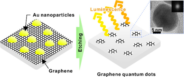
A new graphene quantum dot (GQD) fabrication method is presented, which employs a lithographic approach based on self-assembled Au nanoparticles formed by solid-state dewetting. The GQDs are formed by the patterned etching of a graphene layer enabled by Au nanoparticles, and their size is controllable through that of the Au nanoparticles. GQDs are fabricated with four different diameters: 12, 14, 16, and 27 nm. The geometrical features and lattice structures of the GQDs are determined using transmission electron microscopy (TEM). Hexagonal lattice fringes in the TEM image and G- and 2D-band Raman scattering evidence the graphitic characteristics of the GQDs. The oxygen content can be controlled by thermal reduction under a hydrogen atmosphere. In GQDs, the absorption peak wavelengths in the ultraviolet range tend to decrease as the size of the GQDs decreases. They also exhibit apparent photoluminescence (PL). The PL peak wavelength is approximately 600 nm and becomes shorter as the size of the GQDs decreases. The blue shift in the optical absorption and PL of the smaller GQDs is attributed to the quantum confinement effect. The proposed GQD fabrication method can provide a way to control the physical and chemical properties of GQDs via their size and oxygen content.
1. Introduction
Graphene quantum dots (GQDs) are mono- or few-layer graphene with a lateral dimension less than 100 nm.1,2 The quantum confinement effect in GQDs opens a finite band gap and provides to graphene several intriguing optical, thermal, mechanical, and electrical properties including fluorescence.1,3−5 Fluorescent GQDs with photostability, low toxicity, and biocompatibility have several potential applications such as bioimaging,6,7 drug delivery,8,9 photodynamic therapy,10 photodetectors,11−13 light-emitting diodes,14−16 solar cells,17−19 fuel cells,20,21 etc. Choosing a relevant synthesis method is critical for using GQDs in a desired application as the physical and chemical properties of GQDs are sensitive to their size, doping, defects, atomic edge structure, and surface functionalization,22−25 which are affected by the fabrication methods. Recent theoretical studies have predicted that the energy gap and edge states of GQDs depend on passivation24,25 and doping.26 Oxygen passivation can effectively decrease the energy gap in GQDs, and quantum dot shape, edge termination, and functional groups can influence their dipole moments.24 Shape engineering, edge passivation, and functionalization enable the control of material properties for different applications. For example, the engineered GQD-based type-II heterostructures are beneficial for solar cell applications.25
Recently, a number of GQD synthesis methods have been reported, which can be categorized into two groups in a conventional manner: bottom-up and top-down methods.2,22 Bottom-up methods synthesize GQDs from carbon-containing small precursors. These methods include stepwise organic synthesis,27 pyrolysis of the precursor,28 microwave-assisted hydrothermal method,29,30 chemical vapor deposition,31 etc. The bottom-up approach is generally advantageous for the control of the size and shape of the GQDs and less defect formation; however, this method has narrow process windows and a limited number of usable precursors or solvents. The top-down methods usually cleave the bulk graphite into small flakes. The hydrothermal and solvothermal methods,32,33 ultrasonication,34 microwave-assisted processes,35,36 and chemical/electrochemical exfoliation37−39 belong to this category. This approach is generally simpler and more suitable for mass production than bottom-up methods; however, random cleavage limits size and shape controllability. Size-controllable top-down fabrication methods have been developed using block copolymers (BCPs).40,41 Lee et al. employed self-assembled polystyrene-b-poly(dimethylsiloxane) BCPs to fabricate an array of silica nanoparticles on graphene as an etch hard mask.40 Kim et al. made Au nanoparticles in a hexagonal array from an HAuCl4-containing diblock copolymer.41 However, such methods require a long process time. In addition, the size-dependent optical properties of GQDs have not been demonstrated using these methods.
In this study, we report a novel top-down GQD fabrication method in a simple and fast manner that enables controlling the size of GQDs and optical properties accordingly. This method utilizes self-assembled Au nanoparticles, which are formed by solid-state dewetting (SSD) on the SiO2 intermediate layer.42,43 The Au nanoparticles act as hard masks during the subsequent SiO2 and graphene etching steps, resulting in the formation of GQDs. The geometric features and atomic structures of the GQDs were observed using transmission electron microscopy (TEM). Raman spectroscopy clearly indicates G- and 2D-bands from the GQDs, which are characteristic signatures of graphitic carbon materials. The incorporation of oxygen into GQDs was also revealed by Raman spectroscopy, which occurs at their edges during the oxygen plasma-etching step. Thermal reduction under a hydrogen atmosphere can remove oxygen, and this provides a pathway to control the physical and chemical properties via oxygen content. The optical properties of the reduced GQDs were characterized using ultraviolet–visible (UV/vis) absorption spectroscopy and photoluminescence (PL). The blue shift in both the optical absorption and PL spectra as the size of the GQDs decreases is attributed to the size-dependent quantum confinement effect.
2. Fabrication Process of GQDs Using Self-Assembled Au Nanoparticles
The complete fabrication process is illustrated in Figure 1. The substrate was cleaned with acetone and isopropyl alcohol to remove organic contaminants (Figure 1a). Double-sided polished c-plane sapphire substrates were mainly used in this study. CVD-grown graphene on Cu foils was transferred onto the cleaned substrate (Figure 1b) employing a poly(methyl methacrylate) (PMMA)-assisted Cu etching method.44 The PMMA supporting layer was dissolved in hot acetone (60 °C). PMMA residues were burned by heat treatment at 450 °C under a N2 ambient for 30 min. Note that the formation of GQDs directly on Cu foil without transfer is also possible by following the processes described later.
Figure 1.
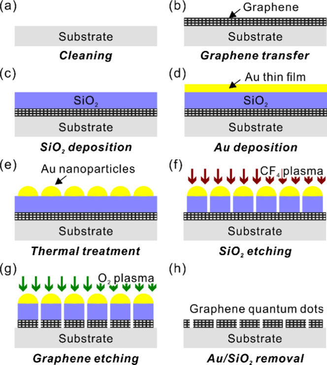
Illustration of the GQD fabrication process using self-assembled Au nanoparticles. (a) Substrate cleaning, (b) graphene transfer to the substrate, (c) deposition of the intermediate SiO2 layer, (d) deposition of the Au thin film, (e) thermal annealing to form Au nanoparticles, (f) SiO2 layer etching by CF4 plasma, (g) graphene etching by O2 plasma, and (h) removal of Au nanoparticles and SiO2 layer.
A 30 nm thick SiO2 layer was deposited on the graphene layer by plasma-enhanced chemical vapor deposition with SiH4 and N2O precursors (Figure 1c). The thin Au film deposition by e-beam evaporation is sketched in Figure 1d. From the thin Au film, nanoparticles were spontaneously generated by rapid thermal annealing in N2 ambient (Figure 1e). We controlled the thickness of the Au film in the range of 2–5 nm, annealing temperature in the range of 300–600 °C, and annealing time in the range of 30–120 s to control the diameters of the Au nanoparticles and improve their dispersion.
The Au nanoparticles were utilized as hard masks in the subsequent SiO2 etching step. The SiO2 layer was etched using inductively coupled plasma reactive ion etching with 10 sccm of CF4 gas (Figure 1f). The etching rate was approximately 0.65 nm/s. Only the graphene exposed on the surface was etched by O2 plasma; however, the one underneath the Au/SiO2 hard mask survived and formed GQDs (Figure 1g). Finally, a 6:1 buffered oxide etchant and a diluted commercial Au etchant removed the SiO2 and Au nanoparticles, respectively, revealing GQDs, as illustrated in Figure 1h. Each wet etching process was followed by rinsing in deionized water for a minute.
3. Results and Discussion
3.1. Self-Assembled Au Nanoparticles
SSD refers to agglomeration in a thin metal film on a substrate, activated to reduce the surface energy of the film and interfacial energy between the film and substrate.42 SSD can be thermally driven through the enhanced surface diffusion of the metal atoms even at temperatures below the melting point of a metal.42 The SSD process parameters (Au film thickness, annealing temperature, and time) are tuned to control the diameters of self-assembled Au nanoparticles, as well as improve their dispersion. Figure 2a–d provides the scanning electron microscopy (SEM) images of Au nanoparticles fabricated under optimal conditions. Each condition produced uniformly dispersed Au nanoparticles of different diameters. The process parameters are presented in Table 1.
Figure 2.
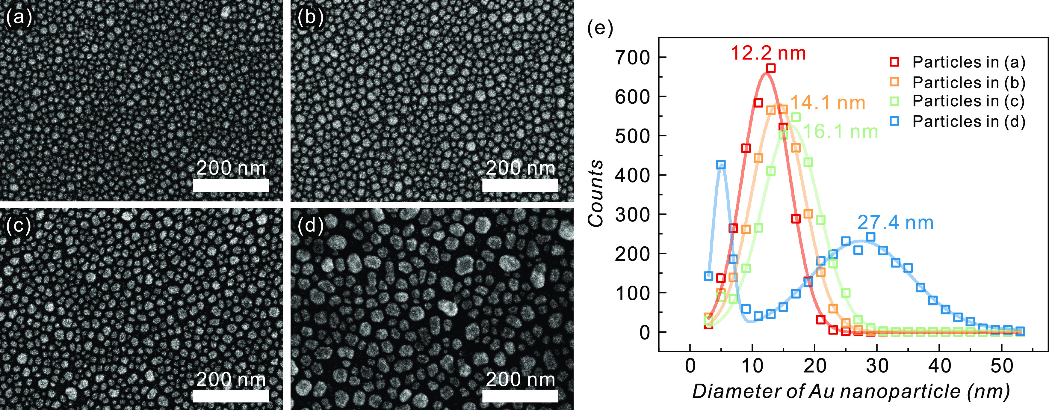
Self-assembled Au nanoparticles. Scanning electron microscopy images of Au nanoparticles made from (a) 2 nm Au film annealed by 500 °C for 2 min, (b) 2.5 nm Au film annealed by 600 °C for 2 min, (c) 3 nm Au film annealed by 400 °C for 2 min, and (d) 5 nm Au film annealed by 300 °C for 30 s. (e) Histogram for the diameter of Au nanoparticles given in panels (a–d).
Table 1. Process Parameters for Fabricating Au Nanoparticlesa,b.
| annealing
condition |
|||||
|---|---|---|---|---|---|
| Au film thickness (nm) | temperature (°C) | time (s) | particle diameter (nm) | σ (nm) | |
| condition A | 2 | 500 | 120 | 12.2 | 7.7 |
| condition B | 2.5 | 600 | 120 | 14.1 | 8.5 |
| condition C | 3 | 300 | 120 | 16.1 | 9.2 |
| condition D | 5 | 400 | 30 | 5.1 | 2.86 |
| 27.4 | 16.0 | ||||
A thin SiO2 layer is crucial for the formation of Au nanoparticles on graphene. On the pristine graphene surface, Au nanoparticles were not uniformly formed, as indicated in Figure S1. This could be attributed to the low interfacial energy between graphene and metal.45 The roughness and thickness of the SiO2 layer affect the formation of Au nanoparticles. On a very thin SiO2 layer (<15 nm), Au nanoparticles were not evenly formed, which was probably due to the rough surface. When using a thick SiO2 layer (>35 nm), the Au nanoparticles could not endure the long SiO2 etching process and failed to act as hard masks.
Figure 2e illustrates the histograms of the distribution of the diameters of the Au nanoparticles, as illustrated in Figure 2a–d. Assuming that a nanoparticle is hemispherical, its diameter can be calculated from the area. Particle diameters and their distributions were determined by the Gaussian fitting and are presented in Table 1. We were able to precisely control the particle diameters between 12 and 16 nm in steps of 2 nm. Both the diameter and distribution tended to increase as the initial Au film thickness increased. We also fabricated larger Au nanoparticles with an average diameter of 27.4 nm. As illustrated by the pale blue line in Figure 2e, small Au nanoparticles (∼5 nm in diameter) survived when forming larger particles. Such small Au particles could not function as hard masks during the SiO2 etching process and lead to small GQDs.
3.2. Geometrical Features of the Fabricated GQDs
The GQDs remained after graphene etching with a Au/SiO2 hard mask, as illustrated in Figure 1h. TEM measurements confirmed the formation of GQDs. Figure 3a illustrates a low-magnification plane-view image of the GQDs on a TEM grid. These GQDs were fabricated directly on a Cu foil without the initial transfer step (Figure 1a,b) and transferred onto a TEM grid from the Cu foil by the PMMA-assisted method described before.
Figure 3.
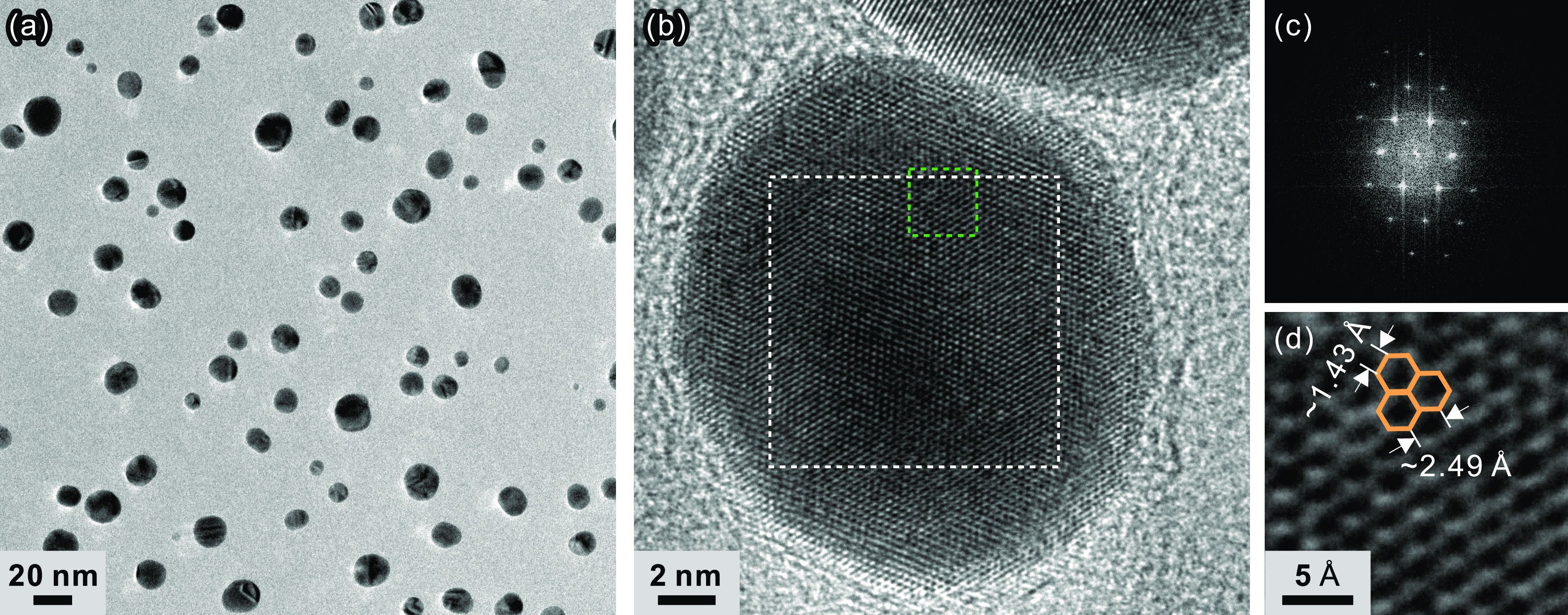
(a) Low-magnification TEM image of the fabricated GQDs dispersed on a TEM grid and (b) high-resolution TEM image of a single GQD. (c) FFT image for the area indicated by the white dotted box and (d) lattice fringes over the green dotted box of panel (b).
In Figure 3a, the most popular diameter of GQDs is ∼14.3 nm and the standard deviation of the GQD diameter is ∼5.9 nm. Since the process parameter has been optimized to minimize the isotropicity of the etching process, the lateral dimension of the SiO2 hard mask is, in principle, one-to-one with that of Au nanoparticles, which is again one-to-one with the diameter of the fabricated GQDs. Consequently, the size of Au nanoparticles and GQDs is similar to each other. It can also be possible to obtain GQDs smaller than Au nanoparticles by increasing the isotropic etching characteristics.
A high-resolution (HR) TEM image of a single GQD is illustrated in Figure 3b, and the corresponding fast Fourier transform (FFT) image of the area indicated by the white dotted box in the figure is illustrated in Figure 3c. The clearly visible lattice fringes in the HR-TEM image and hexagonal structure in the FFT image are consistent with the graphene lattice, and these guarantee the high crystal quality of the fabricated GQDs. The lattice fringes in the green dotted area in Figure 3b are magnified in Figure 3d. The hexagonal lattice fringes are clearly visible. The measured lattice constant (∼2.49 Å) and carbon–carbon bond length (∼1.43 Å) are similar to those of pristine graphene.46 Lattice parameters are obtained from the intensity profile of lattice fringes, as indicated in Figure S2.
3.3. Raman Spectrum of the Fabricated GQDs
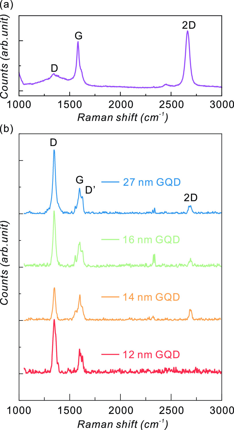
Raman spectra of the GQDs and the graphene have been measured. The results are shown in Figure 4. The wavelength of the incident laser is 532 nm. Figure 4a illustrates the Raman spectrum of the graphene transferred onto a sapphire substrate. The peak around 1580 cm–1 (G-band) is a signature of the sp2-carbon system, which originates from the E2g vibration mode (stretching of the C–C bond in graphitic material) at the Γ-point.47 Disordered structure, impurities, or surface charges in graphene can induce D- and D′-bands, which peak at ∼1350 and ∼1650 cm–1, respectively.48−50 D′-band is attributed to the interaction between the localized defect-related vibration modes and extended vibrational modes of graphene. The 2D-band at ∼2680 cm–1 is a second-order scattering of the D-band, comprising the signature of graphitic carbon materials.49,50 The 2D-band intensity being stronger than the G-band indicates that this sample is mainly a single layer.51 The height of the GQDs is determined by the thickness of the graphene. We do expect that most of the fabricated GQDs will comprise monolayer graphene.
Figure 4.
Raman spectra of (a) graphene and (b) as-fabricated GQDs.
As illustrated in Figure 4b, GQDs show the signature scattering of graphitic material, G- and 2D-band, which is consistent with the preserved graphene lattice of GQDs in the TEM images. The intensities of the G- and 2D-bands decrease because the graphene area is reduced by forming quantum dots. This is a common feature of GQDs made of graphene sheets.40,41 The D-band intensity of GQDs increases remarkably. The enhanced D-band intensity can originate from the generation of edge structures that are inherently disordered in several ways. Similar to the decrease in the G- and 2D-band intensities, an increase in D-band scattering is commonly observed in GQDs.40,41
3.4. Presence of Oxygen in the Fabricated GQDs
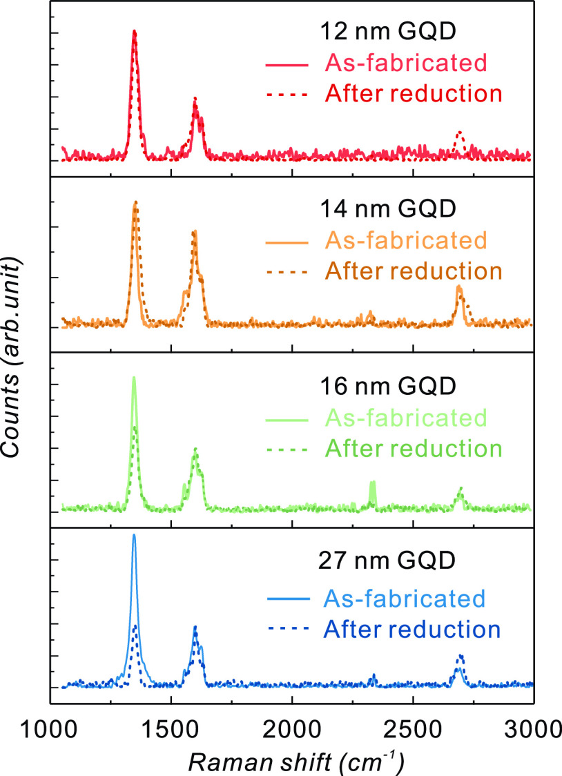
In the Raman spectra of the GQDs illustrated in Figure 4b, the D′-peak at ∼1620 cm–1, which is absent in the Raman spectrum of the transferred graphene film, is present. This can be attributed to the vacancy-like defects at the GQD edges and oxygen impurities in the GQDs.49,50 During oxygen plasma etching, oxygen can be incorporated into GQDs by reacting with the vacancy-like defects present along the exposed edges. Thermal annealing in a reducing atmosphere can remove oxygen impurities from GQDs. Figure 5 shows the Raman spectra of the GQDs before and after thermal reduction at 800 °C in H2 ambient for 10 min. A reduction in defect-related Raman bands, particularly in the D-band, can be observed clearly for 16 nm and 27 nm of GQDs. On the other hand, there is little change in the D-band intensity of the 12 and 14 nm GQDs. The D-band intensity change can be relevant for the modification of the edge structure. A more detailed discussion is available in the Supporting Information based on the intensity ratio between the D-band and G-band before and after thermal treatment (see Figure S3).
Figure 5.
Raman spectra of as-fabricated GQDs and thermally reduced GQDs.
The D′-peak tends to decrease by thermal reduction. The D′-band suppression is attributed to the removal of oxygen atoms. XPS confirmed that the thermal reduction process effectively suppressed the C–O bonding, as shown in Figure S4. The thermal reduction process can sometimes be crucial for obtaining the desired properties because the physical and chemical properties of GQDs can be affected by the oxygen content.
3.5. Optical Properties of the Fabricated GQDs
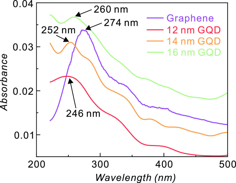
The optical properties of the reduced GQDs were characterized using UV/vis absorption and PL spectroscopy. Figure 6 illustrates the room-temperature optical UV/vis absorption spectra of graphene and GQDs with different diameters. In graphene, the absorption peak at ∼274 nm is attributed to the excitonic effect on the interband transition near the saddle point (M) in the graphene band structure.52,53 An additional small peak seen at ∼320 nm is attributed to the n−π* transition of the carbon–oxygen double bond,54 which may be formed during the oxygen plasma etching performed to remove the graphene on the back side of the Cu foil.
Figure 6.
Optical absorbance of graphene and GQDs with different diameters. The spectra are characterized by a blue shift for smaller diameters of the GQDs.
The predominant absorption peaks of GQDs are blue-shifted compared to those in graphene. The absorption peaks are at 246 nm (5.04 eV), 252 nm (4.92 eV), and 260 nm (4.77 eV) for 12.2, 14.1, and 16.1 nm GQDs, respectively. The absorption peak wavelengths decrease as the size of the GQDs decreases. The optical band gap was calculated using a Tauc plot, as shown in Figure S5. The optical band gap of GQDs decreases from 3.92 to 3.43 eV as their size increases from 12.2 to 16.1 nm. The blue shift can be attributed to the stronger quantum confinement effects in smaller GQDs.
The PL spectra of the GQDs on a sapphire substrate have been measured at a cryogenic temperature (10 K) with an excitation laser wavelength of 365 nm. The GQD diameters of 12.2 and 14.1 nm exhibit 582 nm (2.13 eV) and 599 nm (2.07 eV) luminescence, respectively, as illustrated in Figure 7a. PL emission was not observed for graphene and the GQDs with diameters of 16 and 27 nm. Most PL studies have been conducted with very large numbers of GQDs dispersed in liquid solutions.1−5 PL observation of thin-film-structured GQDs has been challenging because of the limited number of GQDs that should be compensated by the higher quality with fewer defects for effective luminescence. Although measured at a cryogenic temperature, the GQDs exhibited clear and apparent luminescence and size dependence.
Figure 7.
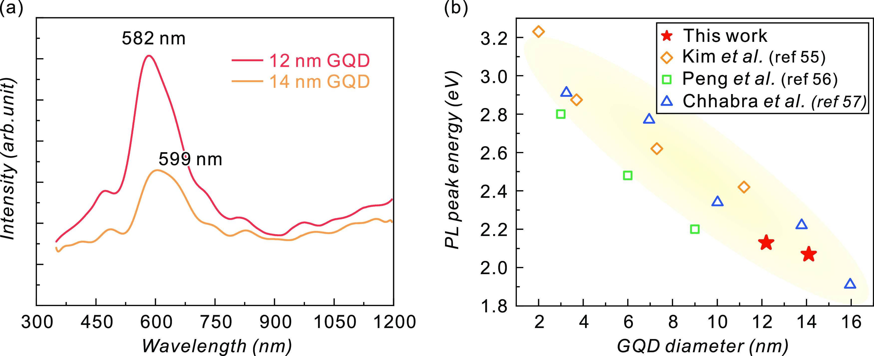
(a) Photoluminescence spectra taken at 10 K from GQDs with diameters of 12 and 14 nm. A shorter PL peak is observed in 12 nm diameter GQDs. (b) Trend of the PL peak energy depending on the diameter of GQDs. These results are consistent with the results in refs (55−57). Reprinted in part from ref (55) with permission from Kim et al., ACS Nano 2012, 6, 8203–8208. Copyright 2012 American Chemical Society, from ref (56) with permission from Peng et al., Nano Lett. 2012, 12, 844–849. Copyright 2012 American Chemical Society, and from ref (56) with permission from Chhabra et al., RSC. Adv. 2018, 8, 11446–11454. Copyright 2018 Royal Society of Chemistry.
The size-dependent luminescence wavelength can behave in a complex way because the emission from GQDs is easily affected not only by their size but also by other variables such as defects, edge structures, and functional groups. If internal defects or disorders exist, the effective GQD volume where the quantum confinement actually emerges can differ from its physical volume, and the PL peak energy will alter accordingly.55 Our method will be bound to limit the generation of defects inside the GQD, owing to hard masks protecting graphene from plasma damage. Therefore, we would expect that the observed change in the PL peak wavelength is mainly caused by the stronger confinement effect in the smaller GQDs. The edge structures are also known to affect the band-gap energy.23 Our GQDs can have a complex edge structure comprising both zigzag and armchair structures as generated by the plasma-etching process.58 Since a zigzag edge is theoretically favored to emit long-wavelength light,23 the zigzag structure may be more dominant in the GQDs over the armchair structure. The observed PL peak energies of the GQDs are in line with the trend observed for the other GQDs, as illustrated in Figure 7b.
It is worth noting that size-controlled high-quality luminescent GQDs were successfully fabricated in this study through simple and fast processes using self-assembled Au nanoparticles. This fabrication method comprises well-established thin-film technologies that are compatible with the conventional lithographic technique; therefore, it is also possible to distribute GQDs only in a specific area through the patterning of Au thin films. Process compatibility allows it to be easily applied to a variety of devices, such as transistors, nonvolatile memories, light-emitting devices, and photodiodes.
This fabrication method also has some challenges. The luminescent properties of GQDs can be tuned by adding a functional group to the edge.22−25 However, the functionalization is limited to an etching-based top-down approach. Postannealing in a reactive atmosphere like post-thermal reduction in this study can be a countermeasure to relieve the limitation. A low throughput is a typical issue in the top-down approaches. The compatibility of the proposed process with the well-established large-scale graphene production technology59 can enable the fabrication of large amounts of GQDs using the proposed method and alleviate the throughput issue.
4. Summary and Conclusions
In summary, GQDs of various sizes have been fabricated by the patterned etching of graphene with self-assembled Au nanoparticles, which were spontaneously formed from thin Au films by SSD. The graphene underneath the Au/SiO2 hard mask was protected from oxygen plasma etching, resulting in the formation of GQDs. The proposed method is simple and faster than other top-down GQD fabrication methods. The formation of the GQDs has been confirmed using microscopic techniques and Raman spectroscopy. The graphitic characteristics of the GQDs were directly observed using TEM and evidenced by G- and 2D-band scattering in Raman spectroscopy. Weak G- and 2D-bands and relatively strong D-band scattering in the Raman spectrum were common features of GQDs, owing to the high ratio of the perimeter to the surface area. The oxygen incorporated into the dots during plasma etching was removed by thermal reduction under a hydrogen atmosphere. The reduced GQDs revealed optical emission and a blue shift in the UV/vis absorption and PL peaks as the diameter of the GQDs decreased. This trend is attributed to the stronger quantum confinement effect in smaller QDs. The proposed method is able to control the physical and chemical properties of GQDs via their size and impurities. In addition to the current thin-film and large-scale graphene production technologies, these new GQDs are expected to show diverse application possibilities.
Acknowledgments
This work was supported by the Basic Science Research Program through the National Research Foundation (NRF) of Korea funded by the Ministry of Education (Grant No. NRF-2020R1I1A3066324). The authors gratefully thank Prof. Jochen Mannhart for editorial comments and Dr. Bhishma Pandit for technical support.
Supporting Information Available
The Supporting Information is available free of charge at https://pubs.acs.org/doi/10.1021/acsomega.2c07683.
SEM images of Au nanoparticles formed on graphene layers (Figure S1); the intensity profiles of GQD’s lattice fringes measured by HR-TEM (Figure S2); the intensity ratio of the D-band to the G-band (ID/IG) of the GQDs before and after thermal reduction (Figure S3); XPS of GQDs before and after thermal reduction (Figure S4); and Tauc plot from the absorbance spectra of GQDS (Figure S5) (PDF)
Author Contributions
§ H.K. and D.Y.K. contributed equally to this work as the first author.
The authors declare no competing financial interest.
Supplementary Material
References
- Wang D.; Chen J. F.; Dai L. M. Recent Advances in Graphene Quantum Dots for Fluorescence Bioimaging from Cells through Tissues to Animals. Part. Part. Syst. Charact. 2015, 32, 515–523. 10.1002/ppsc.201400219. [DOI] [Google Scholar]
- Chen W.; Lv G.; Hu W. M.; Li D. J.; Chen S. N.; Dai Z. X. Synthesis and applications of graphene quantum dots: a review. Nanotechnol. Rev. 2018, 7, 157–185. 10.1515/ntrev-2017-0199. [DOI] [Google Scholar]
- Luk C. M.; Tang L. B.; Zhang W. F.; Yu S. F.; Teng K. S.; Lau S. P. An efficient and stable fluorescent graphene quantum dot–agar composite as a converting material in white light emitting diodes. J. Mater. Chem. 2012, 22, 22378–22381. 10.1039/c2jm35305a. [DOI] [Google Scholar]
- Lin L.; Rong M.; Luo F.; Chen D.; Wang Y.; Chen X. Luminescent graphene quantum dots as new fluorescent materials for environmental and biological applications. TrAC, Trends Anal. Chem. 2014, 54, 83–102. 10.1016/j.trac.2013.11.001. [DOI] [Google Scholar]
- Yoon H.; Park M.; Kim J.; Novak T. G.; Lee S.; Jeon S. Toward highly efficient luminescence in graphene quantum dots for optoelectronic applications. Chem. Phys. Rev. 2021, 2, 031303 10.1063/5.0049183. [DOI] [Google Scholar]
- Zhang M.; Bai L.; Shang W.; Xie W.; Ma H.; Fu Y.; Fang D.; Sun H.; Fan L.; Han M.; Liu C.; Yang S. Facile synthesis of water-soluble, highly fluorescent graphene quantum dots as a robust biological label for stem cells. J. Mater. Chem. 2012, 22, 7461–7467. 10.1039/c2jm16835a. [DOI] [Google Scholar]
- Schroeder K. L.; Goreham R. V.; Nann T. Graphene Quantum Dots for Theranostics and Bioimaging. Pharm. Res. 2016, 33, 2337–2357. 10.1007/s11095-016-1937-x. [DOI] [PubMed] [Google Scholar]
- Iannazzo D.; Ziccarelli I.; Pistone A. Graphene quantum dots: multifunctional nanoplatforms for anticancer therapy. J. Mater. Chem. B 2017, 5, 6471–6489. 10.1039/C7TB00747G. [DOI] [PubMed] [Google Scholar]
- Su Y.-L.; Yu T.-W.; Chiang W. -H.; Chiu H.-C.; Chang C.-H.; Chiang C.-S.; Hu S.-H. Hierarchically Targeted and Penetrated Delivery of Drugs to Tumors by Size-Changeable Graphene Quantum Dot Nanoaircrafts for Photolytic Therapy. Adv. Funct. Mater. 2017, 27, 1700056 10.1002/adfm.201700056. [DOI] [Google Scholar]
- Zhang D.; Wen L.; Huang R.; Wang H.; Hu X.; Xing D. Mitochondrial specific photodynamic therapy by rare-earth nanoparticles mediated near-infrared graphene quantum dots. Biomaterials 2018, 153, 14–26. 10.1016/j.biomaterials.2017.10.034. [DOI] [PubMed] [Google Scholar]
- Zhang Q.; Jie J. S.; Diao S. L.; Shao Z. B.; Zhang Q.; Wang L.; Deng W.; Hu W. D.; Xia H.; Yuan X. D.; Lee S. T. Solution-Processed Graphene Quantum Dot Deep-UV Photodetectors. ACS Nano 2015, 9, 1561–1570. 10.1021/acsnano.5b00437. [DOI] [PubMed] [Google Scholar]
- Bai G.; Tsang M.-K.; Hao J. Luminescent Ions in Advanced Composite Materials for Multifunctional Applications. Adv. Funct. Mater. 2016, 26, 6330–6350. 10.1002/adfm.201602142. [DOI] [Google Scholar]
- Tang L.; Ji R.; Li X.; Bai G.; Liu C. P.; Hao J.; Lin J.; Jiang H.; Teng K. S.; Yang Z.; Lau S. P. Deep Ultraviolet to Near-Infrared Emission and Photoresponse in Layered N-Doped Graphene Quantum Dots. ACS Nano 2014, 8, 6312–6320. 10.1021/nn501796r. [DOI] [PubMed] [Google Scholar]
- Dong P.; Jiang B.-P.; Liang W.-Q.; Huang Y.; Shi Z.; Shen X.-C. Synthesis of white-light-emitting graphene quantum dots via a one-step reduction and their interfacial characteristics-dependent luminescence properties. Inorg. Chem. Front. 2017, 4, 712–718. 10.1039/C6QI00587J. [DOI] [Google Scholar]
- Dai W.; Lei Y.; Xu M.; Zhao P.; Zhang Z.; Zhou J. Rare-Earth Free Self-Activated Graphene Quantum Dots and Copper-Cysteamine Phosphors for Enhanced White Light-Emitting-Diodes under Single Excitation. Sci. Rep. 2017, 7, 12872 10.1038/s41598-017-13404-1. [DOI] [PMC free article] [PubMed] [Google Scholar]
- Zhu J.; Bai X.; Chen X.; Xie Z.; Zhu Y.; Pan G.; Zhai Y.; Zhang H.; Dong B.; Song H. Carbon dots with efficient solid-state red-light emission through the step-by-step surface modification towards light-emitting diodes. Dalton Trans. 2018, 47, 3811–3818. 10.1039/C7DT04579D. [DOI] [PubMed] [Google Scholar]
- Tang Q.; Zhu W.; He B.; Yang P. Rapid Conversion from Carbohydrates to Large-Scale Carbon Quantum Dots for All-Weather Solar Cells. ACS Nano 2017, 11, 1540–1547. 10.1021/acsnano.6b06867. [DOI] [PubMed] [Google Scholar]
- Tsai M. L.; Wei W. R.; Tang L.; Chang H. C.; Tai S. H.; Yang P. K.; Lau S. P.; Chen L. J.; He J. H. Si Hybrid Solar Cells with 13% Efficiency via Concurrent Improvement in Optical and Electrical Properties by Employing Graphene Quantum Dots. ACS Nano 2016, 10, 815–821. 10.1021/acsnano.5b05928. [DOI] [PubMed] [Google Scholar]
- Diao S.; Zhang X.; Shao Z.; Ding K.; Jie J.; Zhang X. 12.35% efficient graphene quantum dots/silicon heterojunction solar cells using graphene transparent electrode. Nano Energy 2017, 31, 359–366. 10.1016/j.nanoen.2016.11.051. [DOI] [Google Scholar]
- Dhand A.; Suresh S.; Jain A.; Varadan O. N.; Kerawalla M. A. K.; Goswami P. Advances in Materials for Fuel Cell Technologies-A Review. Int. J. Res. Appl. Sci. Eng. Technol. 2017, 5, 1672–1682. 10.22214/ijraset.2017.9243. [DOI] [Google Scholar]
- Fei H.; Ye R. Q.; Ye G. L.; Gong Y. J.; Peng Z. W.; Fan X. J.; Samuel E. L. G.; Ajayan P. M.; Tour J. M. Boron- and Nitrogen-Doped Graphene Quantum Dots/Graphene Hybrid Nanoplatelets as Efficient Electrocatalysts for Oxygen Reduction. ACS Nano 2014, 8, 10837–10843. 10.1021/nn504637y. [DOI] [PubMed] [Google Scholar]
- Zhu S.; Song Y.; Wang J.; Wan H.; Zhang Y.; Ning Y.; Yang B. Photoluminescence mechanism in graphene quantum dots: Quantum confinement effect and surface/edge state. Nano Today 2017, 13, 10–14. 10.1016/j.nantod.2016.12.006. [DOI] [Google Scholar]
- Li Y.; Shu H.; Wang S.; Wang J. Electronic and Optical Properties of Graphene Quantum Dots: The Role of Many-Body Effects. J. Phys. Chem. C 2015, 119, 4983–4989. 10.1021/jp506969r. [DOI] [Google Scholar]
- Abdelsalam H.; Elhaes H.; Ibrahim M. A. Tuning electronic properties in graphene quantum dots by chemical functionalization: Density functional theory calculation. Chem. Phys. Lett. 2018, 695, 138–148. 10.1016/j.cplett.2018.02.015. [DOI] [Google Scholar]
- Abdelsalam H.; Atta H. M.; Osman W.; Zhang Q. Two-dimensional quantum dots for highly efficient heterojunction solar cells. J. Colloid Interface Sci. 2021, 603, 48–57. 10.1016/j.jcis.2021.06.121. [DOI] [PubMed] [Google Scholar]
- Osman W.; Abdelsalam H.; Ali M.; Teleb N. H.; Yahia I. S.; Ibrahim M. A.; Zhang Q. Electronic and magnetic properties of graphene quantum dots doped with alkali metals. J. Mater. Res. Technol. 2021, 11, 1517–1533. 10.1016/j.jmrt.2021.01.119. [DOI] [Google Scholar]
- Tian R.; Zhong S.; Wu J.; Geng Y.; Zhou B.; Wang Q.; Jiang W. Facile preparation and the stepwise formation mechanistic investigation of gram-scale nitrogen-doped graphene quantum dots. J. Mater. Chem. C 2017, 5, 9174–9180. 10.1039/C7TC02434G. [DOI] [Google Scholar]
- Naik J. P.; Sutradhar P.; Saha M. Molecular scale rapid synthesis of graphene quantum dots (GQDs). J. Nanostruct. Chem. 2017, 7, 85–89. 10.1007/s40097-017-0222-9. [DOI] [Google Scholar]
- Choi Y.; Thongsai N.; Chae A.; Jo S.; Kang E. B.; Paoprasert P.; Park S. Y.; In I. Microwave-assisted synthesis of luminescent and biocompatible lysine-based carbon quantum dots. J. Ind. Eng. Chem. 2017, 47, 329–335. 10.1016/j.jiec.2016.12.002. [DOI] [Google Scholar]
- Borse V.; Thakur M.; Sengupta S.; Srivastava R. N-doped multi-fluorescent carbon dots for ‘turn off-on’ silver-biothiol dual sensing and mammalian cell imaging application. Sens. Actuators, B 2017, 248, 481–492. 10.1016/j.snb.2017.03.158. [DOI] [Google Scholar]
- Fan L.; Zhu M.; Lee X.; Zhang R.; Wang K.; Wei J.; Zhong M.; Wu D.; Zhu H. Direct Synthesis of Graphene Quantum Dots by Chemical Vapor Deposition. Part. Part. Syst. Charact. 2013, 30, 764–769. 10.1002/ppsc.201300125. [DOI] [Google Scholar]
- Pan D.; Zhang J.; Li Z.; Wu M. Hydrothermal Route for Cutting Graphene Sheets into Blue-Luminescent Graphene Quantum Dots. Adv. Mater. 2010, 22, 734–738. 10.1002/adma.200902825. [DOI] [PubMed] [Google Scholar]
- Tetsuka H.; Asahi R.; Nagoya A.; Okamoto K.; Tajima I.; Ohta R.; Okamoto A. Optically Tunable Amino-Functionalized Graphene Quantum Dots. Adv. Mater. 2012, 24, 5333–5338. 10.1002/adma.201201930. [DOI] [PubMed] [Google Scholar]
- Zhu Y.; Wang G.; Jiang H.; Chen L.; Zhang X. One-step ultrasonic synthesis of graphene quantum dots with high quantum yield and their application in sensing alkaline phosphatase. Chem. Commun. 2015, 51, 948–951. 10.1039/C4CC07449A. [DOI] [PubMed] [Google Scholar]
- Li L.-L.; Ji J.; Fei R.; Wang C.-Z.; Lu Q.; Zhang J.-R.; Jiang L.-P.; Zhu J.-J. A Facile Microwave Avenue to Electrochemiluminescent Two-Color Graphene Quantum Dots. Adv. Funct. Mater. 2012, 22, 2971–2979. 10.1002/adfm.201200166. [DOI] [Google Scholar]
- Zhang C.; Cui Y.; Song L.; Liu X.; Hu Z. Microwave assisted one-pot synthesis of graphene quantum dots as highly sensitive fluorescent probes for detection of iron ions and pH value. Talanta 2016, 150, 54–60. 10.1016/j.talanta.2015.12.015. [DOI] [PubMed] [Google Scholar]
- Tan X.; Li Y.; Li X.; Zhou S.; Fan L.; Yang S. Electrochemical synthesis of small-sized red fluorescent graphene quantum dots as a bioimaging platform. Chem. Commun. 2015, 51, 2544–2546. 10.1039/C4CC09332A. [DOI] [PubMed] [Google Scholar]
- Shinde D. B.; Pillai V. K. Electrochemical Preparation of Luminescent Graphene Quantum Dots from Multiwalled Carbon Nanotubes. Chem.- Eur. J. 2012, 18, 12522–12528. 10.1002/chem.201201043. [DOI] [PubMed] [Google Scholar]
- Shinde D. B.; Dhavale V. M.; Kurungot S.; Pillai V. K. Electrochemical preparation of nitrogen-doped graphene quantum dots and their size-dependent electrocatalytic activity for oxygen reduction. Bull. Mater. Sci. 2015, 38, 435–442. 10.1007/s12034-014-0834-3. [DOI] [Google Scholar]
- Lee J.; Kim K.; Park W. I.; Kim B. H.; Park J. H.; Kim T. H.; Bong S.; Kim C. H.; Chae G.; Jun M.; Hwang Y.; Jung Y. S.; Jeon S. Uniform Graphene Quantum Dots Patterned from Self-Assembled Silica Nanodots. Nano. Lett. 2012, 12, 6078–6083. 10.1021/nl302520m. [DOI] [PubMed] [Google Scholar]
- Kim S. S.; Choi J. Y.; Kim K.; Sohn B. H. Large area tunable arrays of graphene nanodots fabricated using diblock copolymer micelles. Nanotechnology 2012, 23, 125301 10.1088/0957-4484/23/12/125301. [DOI] [PubMed] [Google Scholar]
- Seguini G.; Curi J. L.; Spiga S.; Tallarida G.; Wiemer C.; Perego M. Solid-state dewetting of ultra-thin Au films on SiO2 and HfO2. Nanotechnology 2014, 25, 495603 10.1088/0957-4484/25/49/495603. [DOI] [PubMed] [Google Scholar]
- Gadkari P. R.; Warren A. P.; Todi R. M.; Petrova R. V.; Coffey K. R. Comparison of the agglomeration behavior of thin metallic films on SiO2. J. Vac. Sci. Technol., A 2005, 23, 1152–1161. 10.1116/1.1861943. [DOI] [Google Scholar]
- Li X.; Zhu Y.; Cai W.; Borysiak M.; Han B.; Chen D.; Piner R. D.; Colombo L.; Ruoff R. S. Transfer of Large-Area Graphene Films for High-Performance Transparent Conductive Electrodes. Nano Lett. 2009, 9, 4359–4363. 10.1021/nl902623y. [DOI] [PubMed] [Google Scholar]
- Dong A.; Fu Q.; Wei M.; Bao X. Graphene-metal interaction and ist effect on the interface stability under ambient conditions. Appl. Surf. Sci. 2017, 412, 262–270. 10.1016/j.apsusc.2017.03.240. [DOI] [Google Scholar]
- Yang G.; Li L.; Lee W. B.; Ng M. C. Structure of graphene and ist disorders: a review. Sci. Technol. Adv. Mater. 2018, 19, 613–648. 10.1080/14686996.2018.1494493. [DOI] [PMC free article] [PubMed] [Google Scholar]
- Ferrari A. C.; Robertson J. Raman spectroscopy of amorphous, nanostructured, diamond-like carbon, and nanodiamond. Philos. Trans. R. Soc., A 2004, 362, 2477–2512. 10.1098/rsta.2004.1452. [DOI] [PubMed] [Google Scholar]
- Cançado L. G.; Pimenta M. A.; Neves B. R.; Dantas M. S.; Jorio A. Influence of the Atomic Structure on the Raman Spectra of Graphite Edges. Phys. Rev. Lett. 2004, 93, 247401 10.1103/PhysRevLett.93.247401. [DOI] [PubMed] [Google Scholar]
- Gao G.; Liu D.; Tang S.; Huang C.; He M.; Guo Y.; Sun X.; Gao B. Heat-Initiated Chemical Functionalization of Graphene. Sci. Rep. 2016, 6, 20034 10.1038/srep20034. [DOI] [PMC free article] [PubMed] [Google Scholar]
- Wu J. B.; Lin M. L.; Cong X.; Liu H. N.; Tan P. H. Raman spectroscopy of graphene-based materials and its applications in related devices. Chem. Soc. Rev. 2018, 47, 1822–1873. 10.1039/C6CS00915H. [DOI] [PubMed] [Google Scholar]
- Calizo I.; Bejenari I.; Rahman M.; Liu G.; Balandin A. A. Ultraviolet Raman microscopy of single and multilayer graphene. J. Appl. Phys. 2009, 106, 043509 10.1063/1.3197065. [DOI] [Google Scholar]
- Yang Li.; Deslippe J.; Park C.-H.; Cohen M. L.; Louie S. G. Excitonic Effects on the Optical Response of Graphene and Bilayer Graphene. Phys Rev. Lett. 2009, 103, 186802 10.1103/PhysRevLett.103.186802. [DOI] [PubMed] [Google Scholar]
- Chae D.-H.; Utikal T.; Weisenburger S.; Giessen H.; Klitzing K. V.; Lippitz M.; Smet J. Excitonic Fano Resonance in Free-Standing Graphene. Nano Lett. 2011, 11, 1379–1382. 10.1021/nl200040q. [DOI] [PubMed] [Google Scholar]
- Paredes J. I.; Villar-Rodil S.; Martinez–Alonso A.; Tascon J. M. D. Graphene Oxide Dispersions in Organic Solvents. Langmuir 2008, 24, 10560–10564. 10.1021/la801744a. [DOI] [PubMed] [Google Scholar]
- Kim S.; Hwang S. W.; Kim M. K.; Shin D. Y.; Shin D. H.; Kim C. O.; Yang S. B.; Park J. H.; Hwang E.; Choi S. H.; Ko G.; Sim S.; Sone C.; Choi H. J.; Bae S.; Hong B. H. Anomalous Behaviors of Visible Luminescence from Graphene Quantum Dots: Interplay between Size and Shape. ACS Nano 2012, 6, 8203–8208. 10.1021/nn302878r. [DOI] [PubMed] [Google Scholar]
- Peng J.; Gao W.; Gupta B. K.; Liu Z.; Romero-Aburto R.; Ge L.; Song L.; Alemany L. B.; Zhan X.; Gao G.; Vithayathil S. A.; Kaipparettu B. A.; Marti A. A.; Hayashi T.; Zhu J. J.; Ajayan P. M. Graphene Quantum Dots Derived from Carbon Fibers. Nano Lett. 2012, 12, 844–849. 10.1021/nl2038979. [DOI] [PubMed] [Google Scholar]
- Chhabra V. A.; Kaur R.; Kumar N.; Deep A.; Rajesh C.; Kim K.-H. Synthesis and spectroscopic studies of functionalized graphene quantum dots with diverse fluorescence characteristics. RSC. Adv. 2018, 8, 11446–11454. 10.1039/C8RA01148F. [DOI] [PMC free article] [PubMed] [Google Scholar]
- Lucchese M. M.; Stavale F.; Ferreira E. H. M.; Vilani C.; Moutinho M. V. O.; Capaz R. B.; Achete C. A.; Jorio A. Quantifying ion-induced defects and Raman relaxation length in graphene. Carbon 2010, 48, 1592–1597. 10.1016/j.carbon.2009.12.057. [DOI] [Google Scholar]
- Bubnova O. A decade of R2R graphene manufacturing. Nat. Nanotechnol. 2021, 16, 1050 10.1038/s41565-021-00990-5. [DOI] [PubMed] [Google Scholar]
Associated Data
This section collects any data citations, data availability statements, or supplementary materials included in this article.


