

Abstract

In the quest for new and increasingly efficient photon sources, the engineering of the photonic environment at the subwavelength scale is fundamental for controlling the properties of quantum emitters. A high refractive index particle can be exploited to enhance the optical properties of nearby emitters without decreasing their quantum efficiency, but the relatively modest Q-factors (Q ∼ 5–10) limit the local density of optical states (LDOS) amplification achievable. On the other hand, ultrahigh Q-factors (up to Q ∼ 109) have been reported for quasi-BIC modes in all-dielectric nanostructures. In the present work, we demonstrate that the combination of quasi-BIC modes with high spectral confinement and nanogaps with spacial confinement in silicon slotted nanoantennas lead to a significant boosting of the electromagnetic LDOS in the optically active region of the nanoantenna array. We observe an enhancement of up to 3 orders of magnitude in the photoluminescence intensity and 2 orders of magnitude in the decay rate of the Er3+ emission at room temperature and telecom wavelengths. Moreover, the nanoantenna directivity is increased, proving that strong beaming effects can be obtained when the emitted radiation couples to the high Q-factor modes. Finally, via tuning the nanoanntenna aspect ratio, a selective control of the Er3+ electric and magnetic radiative transitions can be obtained, keeping the quantum efficiency almost unitary.
Keywords: all-dielectric nanoantenna, quasi-BIC, erbium, decay rate enhancement, nanoslot, metasurface
Introduction
In the weak coupling regime the spontaneous decay rate of an emitter can be modified acting on its electric and magnetic local density of optical states (LDOS), with the magnitude of the radiative emission rate enhancement defined by the Purcell factor (Fp).1−3 In recent years, several different designs and configurations of plasmonic nanoantennas and nanocavities have been studied and strong emission enhancements have been obtained.4−7 Nevertheless, the presence of a metal nanostructure near the emitter induces also quenching phenomena due to nonradiative energy transfer, thus considerably decreasing the quantum efficiency of the emitting system.8−11 This makes plasmonic nanoantennas unsuitable for the realization of high-efficiency photon sources necessary for many cutting-edge applications (e.g., single-photon emitters).12 Recently, all-dielectric high refractive index nanostructures have attracted increasing interest due to their unique optical properties (i.e., low absorption, optical magnetism, and multipolar responses),13−16 which can be exploited to enhance the optical properties of a nearby emitter without decreasing its quantum efficiency.17−21 However, the relatively modest Q-factors exhibited by electric and magnetic Mie resonances in nanoparticles such as spheres or cylinders (Q ∼ 5–10) have limited the performance of high-index nanostructures in the amplification of the LDOS for resonantly coupled quantum emitters.22,23 A possible way to obtain orders of magnitude higher Q-factors (up to Q ∼ 109) in all-dielectric nanostructures is based on optical bound states in the continuum (BICs).24−26 Although true BIC can exist only in structures that are infinitely extended, finite-size systems can support their analog in the form of quasi-BICs.27,28 Nanostructures supporting optical quasi-BICs have already demonstrated their ability to outperform traditional photonic nanoparticles for many photophysical processes usually limited either by losses or by low Q-factor resonances, such as second- and third-harmonic generation, lasing, light guiding, beam shaping, and sensing.29−34 Beside high Q, a large Purcell factor requires an ultrasmall mode volume, a concept exploited in many nanoantennas.35,36 A nanoslot can do this by exploiting electromagnetic field enhancement at the dielectric discontinuities.20,37,38 While combining two resonant antennas usually spoils the collective effect, due to possible interference,39 the not-resonant character of nanogaps can be exploited to obtain a synergistic effect.
Here we propose to combine a high Q-factor quasi-BIC with a nanogap. A thin (30 nm) low-index oxide layer doped with quantum emitters (i.e., Er-doped silica) is placed inside high-index slotted silicon nanopillars arranged in a square array. We choose erbium ions in silica as the emitting medium since Er3+ can be seen as the ideal candidate for the development of novel photonic quantum sources operating at telecom wavelengths,40 due to the sharp room-temperature emission at λ = 1540 nm, that matches the silica minimum absorption window.41 We show that the combination of the nanoslot geometry and the quasi-BIC modes can be exploited to boost the electromagnetic LDOS in the optically active region of the nanoantenna. We demonstrate that by coupling the NIR Er3+ radiative emission with quasi-BIC resonances supported by silicon slotted nanopillars an enhancement of 2 orders of magnitude of the decay rate and almost 3 orders of magnitude of the photoluminescence intensity can be obtained at room temperature. Furthermore, acting on the nanopillars aspect ratio, a selective control of the Er3+ electric and magnetic radiative transitions has been obtained, keeping the quantum efficiency almost unitary. Finally, it was possible also to design and control the emission directivity from the Er:SiO2 nanoslot, focusing ∼90% of the total Er3+ emitted radiation at λ = 1540 nm in a lobe normal to the sample surface with an angular width of Δθ ∼ 10°.
Results and Discussion
Figure 1a shows a sketch of the structure of the samples. The emitting layer, a 30 nm thick nanodisk of silica doped with erbium, is placed at half height of the silicon nanopillars arranged in a square array on a silica substrate. The total nanopillar height is h = 200 + 30 + 200 = 430 nm. The lattice parameter was set as a0 = 800 nm and the radius of the nanopillars was varied in the range r = 250–350 nm. A second set of samples were fabricated with a larger lattice parameter (a0 = 1000 nm) and a broader range of pillar radii (i.e., from r = 125 to 390 nm), keeping h = 430 nm. Thus, the nanopillar aspect ratio (AR = d/h, being d the diameter) was varied from AR = 0.58 to 1.8. An SEM image of the sample with r = 220 nm and a0 = 1000 nm is reported in Figure 1b. The comparison between experimental and simulated transmittance spectra at normal incidence in the 1100–1800 nm wavelength range is reported in Figure S1 of the Supporting Information for the set of samples with a0 = 1000 nm. The silicon dielectric function used for the simulations was determined by ellipsometry measuring an unpatterned region of the sample. A good agreement between simulated and measured transmittance spectra can be observed.
Figure 1.

(a) Sketch of the sample structure. (b) SEM image of the sample with r = 220 nm and a0 = 1000 nm (plane view). (c) Simulated radiative decay rate with averaged ED and MD components for an isotropic emitter (continuous lines) and experimentally measured Er3+ decay rate (dots) in the confocal setup (NA = 0.85). Green and purple colors indicate the nanopillar array with a0 = 800 and 1000 nm, respectively. The orange dashed line indicates the Er3+ radiative decay rate in bulk silica. (d) Purcell factor in SiO2 at λ = 1540 nm for an ED (red) and MD (blue) emitter at the center of the SiO2 nanoslot. Inset: electric (ηED) and magnetic (ηMD) dipole branching ratio as a function of the nanopillar diameter.
We investigated the influence of the high-index nanoantenna aspect ratio on the broadband LDOS enhancement in the nanoslot due to the dielectric discontinuities. We demonstrated that more than 1 order of magnitude decay rate enhancement can be obtained for a 30 nm thick slot in the NIR spectral region and that electric and magnetic LDOS exhibit maxima for different silicon nanopillar aspect ratios. Due to the broadband nature of the nanoslot LDOS enhancement, we choose to study the variation of the decay rate at λ = 1540 nm, i.e., the peak wavelength for the 4I13/2 → 4I15/2 Er3+ transition in silica. The measured Er3+ decay rate at λ = 1540 nm as a function of the nanopillar radius is reported in Figure 1c. The purple and green dots indicate samples with a0 = 800 nm and a0 = 1000 nm, respectively. The orange dashed line shows the radiative decay rate of Er3+ emitters in a homogeneous SiO2 matrix (i.e., Γ0,r = 100 s–1).20 FEM simulated decay rates for a single dipole emitter (λ = 1540 nm) are shown in Figure 1c for the nanopillar arrays with a0 = 800 nm and a0 = 1000 nm, purple and green continuous lines, respectively. It is worth underlining that the 4I13/2 → 4I15/2 Er3+ transition has an almost equal contribution of electric dipole and magnetic dipole components42 and therefore the radiative decay rate variation at λ = 1540 nm was calculated by averaging 50–50 the ED and MD decay rates each of which averaged over the 3 spacial directions (i.e., γave(ED,MD) = 1/3γ⊥ + 2/3γ∥(ED,MD)). To avoid an ambiguous notation, γ is used to indicate the calculated decay rate, while Γ stands for the experimental one. A strong variation of the Er3+ decay rate as a function of the slotted nanopillar aspect ratio can be observed. In the explored diameter range, indeed, the measured decay rate varies in the range Γ ∼ 200–1400 s–1 exhibiting two distinct maxima at r = 220 nm (Γexp = 1350 ± 50 s–1) and at r = 380 nm (Γexp = 950 ± 50 s–1), and a local minimum at r = 325 nm (Γexp = 500 ± 30 s–1). For nanostructures with r < 220 nm the LDOS enhancement in the nanoslot decreases rapidly, reaching the value Γexp = 210 ± 10 s–1 at r = 125 nm. The small difference between the decay rates calculated with a0 = 800 nm and a0 = 1000 nm (see green and purple curves in Figure 1c) indicates that the lattice parameter has a minor influence on the Purcell factor enhancement at λ = 1540 nm. Besides, nanopillar arrays with a similar aspect ratio (e.g., AR ∼ 1.4) but with a different lattice parameter a0 exhibit almost equal decay rates, further confirming that the lattice parameter does not play a crucial role in the Er3+ LDOS enhancement at λ = 1540 nm for this nanophotonic system. It is worth underlining that a decay rate enhancement of more than an order of magnitude has been measured for all-dielectric nanopillars with r = 220 and 390 nm.
To further understand the influence of the aspect ratio of the designed nanoantenna on the electromagnetic LDOS variation in the nanoslot, a set of FEM simulations with electric (ED) and magnetic (MD) dipoles (λem = 1540 nm) at the center of the SiO2 nanoslot have been computed varying the nanopillar radius from r = 125 nm to 390 nm, keeping a0 = 1000 nm. Figure 1d reports the computed Purcell factor (Fp) in the SiO2 nanoslot for ED and MD emitters (red and blue curves, respectively) with averaged orientation, i.e., the deconvolution of the green curve in Figure 1c obtained by averaging the electric and magnetic dipole configurations. Figure S2 of the Supporting Information reports the variation of the Purcell factor with respect to the electric and magnetic dipole position inside the silica nanoslot. Although the displacement of the emitter inside the SiO2 nanodisk has an influence on the LDOS enhancement, a dipole in the center of the nanoslot with averaged orientation represents a good approximation for the evaluation of the radiative decay rate variation in a SiO2 nanoslot homogeneously doped with Er3+. The simulated radiative decay rate enhancement for MD emitters presents a maximum at r = 220 nm (Fp = 24). Conversely, electric dipoles exhibit lower Purcell factors with a maximum of Fp = 17 for nanopillars with r = 375 nm. The influence of the number of neighboring nanostructures (finite-size effect) on the decay rate modification has been evaluated by simulating a set of non periodic configurations with a growing number of pillars arranged in a square array with a0 = 1000 nm around the central one with the emitter (i.e., 1, 9, 25, and 49 pillars in the configuration). The results are reported in Figure S3 of the Supporting Information. The simulated Purcell factor is almost unaffected by the presence of the first, second, and third nearest neighbors square shell in the simulation domain, confirming that the periodic lattice has a small influence on the slotted nanopillar electric and magnetic Purcell factor. The simulated emission system has a unitary quantum efficiency due to the lossless nature of the nanoantenna materials. This has been confirmed by the good agreement between computed and measured values of the decay rate for the whole range of nanopillar radii explored (i.e., green and purple lines vs dots in Figure 1c), indicating that negligible nonradiative decay channels are introduced by the nanoantennas fabrication (i.e., we can assume for Er3+ ions a nonradiative rate Γnr ∼ 0 s–1). This point is of paramount importance not only in terms of the PL intensity enhancement but also concerning advanced photonic applications where nonradiative losses are simply not allowed (e.g., single photon sources). The inset of Figure 1d shows the influence of the nanopillar radius on the electric and magnetic branching ratio, defined as the ratio of the electric (magnetic) radiative decay rate and the total decay rate of the emitter (i.e., ηED = γaveED/γave, ηMD = γaveMD/γave, where γavetot = γave + γaveMD). A strong modulation of the electric and magnetic dipole contribution to the Er3+ radiative transitions can be observed as a function of the nanostructure aspect ratio. A magnetic branching ratio of ηMD = 0.85 can be calculated for nanopillars, with r = 220 nm and an electric one of ηED = 0.82 for r = 375 nm in correspondence to the γave and γaveED maxima, respectively. Such tunability could be exploited for the selective enhancement of electric or magnetic radiative transitions for emitters with mixed nature such as other rare-earth ions with different ED and MD relative contribution to a specific transition.43 The obtained values are much higher than the ones achievable with planar dielectric films with similar slotted structure20 and than the ones measured in Reference44 for a rare-earth doped thin film deposited on top of a high-index nanopillar array (i.e., γMD/γED varies from 0.6 to 1.2). In our nanopillar array, ηMD/ηED = γave/γaveED ranges from 0.2 to 6.2, demonstrating the superiority of the slot geometry for the effective branching ratio modulation. The strong ED- and MD-selective emission acceleration obtained keeping at the same time the Er3+ quantum efficiency close to unity represents an important advantage of the investigated all-dielectric slot nanoantennas with respect to plasmonic nanostructures45,46 for applications in quantum photonics which require fast and highly efficient emitters.
Even if the increase of the quantum efficiency is mainly controlled by the single nanopillar, the emission directivity and decay rate can be further enhanced by the presence of the nanopillar periodicity. Indeed, ordered arrays of silicon nanopillars arranged in a peculiar resonant configuration can support quadrupolar quasi-BIC modes with huge Q-factors (up to Q = 109) in the NIR spectral range.24,26,27 Thanks to the slotted nanoantenna geometry, in the present work we have exploited quasi-BIC resonances to boost the Er3+ radiative emission. Figure 2a shows the PL emission spectrum in the 1400–1650 nm wavelength range for the sample with r = 360 nm and a0 = 800 nm. We have seen that the characteristic Er3+ luminescence spectrum in SiO2 (indicated by the red continuous line) is altered by the appearance of three additional sharp peaks at λ = 1450, 1487, and 1600 nm (blue lines). By the multiple peak analysis, a Q-factor of ∼180 has been calculated for the most intense peak at λ = 1487 nm. This is a clear evidence of the coupling of the Er3+ emission with sharp high-Q modes supported by the nanoantennas array. The spectral width and the PL intensity of the peak are strongly influenced by the wavelength resolution of the experimental setup (i.e., monochromator slits width) and the numerical aperture of the collection lens. Indeed, the peak intensity and its sharpness are maximized for the smallest collection angle and slits width (see Figure S4(a)), indicating that the measured Q-factor can be seen as a lower bound for the true Q-factor, which is strongly underestimated due to the finite angular and spectral resolution of the detection setup.
Figure 2.

(a) PL emission spectrum of the sample with r = 360 nm, a0 = 800 nm (black line), characteristic PL spectrum of Er3+ in SiO2 (red line), and peaks associated with the nanopillar modes (blue line). (b) Normalized PL temporal decay for the nanopillar with r = 360 nm at λ = 1540 and 1487 nm (red and blue dots, respectively) and for a 30 nm thick Er:SiO2 film on the SiO2 substrate at λ = 1540 nm (orange dots). The continuous lines are the exponential fits. (c) Wavelength vs angle map of the simulated averaged electric field intensity enhancement in the SiO2 nanoslot for a TM-polarized plane wave impinging on the nanopillar array, for the sample with r = 360 nm and a0 = 800 nm. The blue arrows indicate the high Q-modes at normal incidence. In (d), a zoom-in view of the region marked with the red square is reported. (e) Simulated Q-factor and line width of the quasi-BIC resonance as a function of the incidence angle. (f) Calculated electric and magnetic field enhancement in the nanoslot at λ = 1487 nm at normal incidence.
In addition to the LDOS increment due to the high-index
slot geometry
(as reported in Figure 1c and discussed above), the efficient spectral coupling of the emitters
in the nanoslot with quasi-BIC resonances has been exploited to further
accelerate the Er3+ radiative emission. Figure 2b reports the normalized PL
temporal decay at λ = 1540 and 1487 nm for the nanopillar array
with r = 360 nm and a0 = 800 nm. The decay curve at λ = 1487 nm is well fitted by
a double exponential decay function, 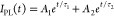 (with A1 + A2 = 1), with a dominant short lifetime component
with A1 = 0.90 ± 0.02 and τ1 = 150 ± 10 μs and a contribution of a longer component
about 10 times smaller (i.e., A2 = 0.10
± 0.02 and τ2 = 1.40 ± 0.05 ms). Conversely,
at λ = 1540 nm the amplitude of the τ1 component
results almost negligible (i.e., A1 ∼
0), and the PL decay is mainly due to the τ2 = 1.40
± 0.05 ms component. This is proof that in correspondence to
the quasi-BIC resonance at λ = 1487 nm an order of magnitude
stronger decay rate has been obtained (Γ1 = 6600
± 400 s–1) with respect to the one measured
off-resonance at λ = 1540 nm (Γ2 = 710 ±
30 s–1). The influence of the numerical aperture
of the collection lens and monochromator slits widths on the lifetime
estimation is reported in Figure S4(b) of the Supporting Information, pointing out that the contribution
of the τ1 component at λ = 1487 nm becomes
predominant upon the increase of the wavelength and angle resolution
of the experimental setup.47,48 This provides clear
evidence that the huge emission amplification is due to an effective
coupling of the Er3+ emission with a mode supported by
the array with a high quality factor (i.e., quasi-BIC resonance).
The orange curve in Figure 2b indicates the decay rate of a reference sample with a 30
nm thick Er:SiO2 film on the silica substrate, fitted with
a single exponential curve with τ0 = 14.0 ±
0.5 ms (Γ0 = 70 ± 3 s–1).
The measured decay rate is in good agreement with the values reported
in the literature for Er-doped thin films on the SiO2 substrate,41,49 proving the high quantum efficiency of the deposited Er:SiO2 layer. Moreover, the good agreement between experiments and
FEM simulations at λ = 1540 nm for the whole range of nanopillar
radii and lattice parameters explored (see Figure 1c) demonstrates that the almost unitary quantum
efficiency of the Er:SiO2 layer is preserved also after
the patterning step necessary for the nanoantenna fabrication. Decay
rate measurements have clearly demonstrated that the proposed nanoantenna
design can support a strong light–matter interaction inside
the SiO2 slot, especially when the emitter couples with
quasi-BIC modes. At the resonance condition, indeed, a Purcell factor
of 2 orders of magnitude has been measured at room temperature (i.e.,
Γ1/Γ0 = 94) for a lossless nanostructure
(i.e., Γnr ∼ 0 s–1 and Q.E.
∼ 1).
(with A1 + A2 = 1), with a dominant short lifetime component
with A1 = 0.90 ± 0.02 and τ1 = 150 ± 10 μs and a contribution of a longer component
about 10 times smaller (i.e., A2 = 0.10
± 0.02 and τ2 = 1.40 ± 0.05 ms). Conversely,
at λ = 1540 nm the amplitude of the τ1 component
results almost negligible (i.e., A1 ∼
0), and the PL decay is mainly due to the τ2 = 1.40
± 0.05 ms component. This is proof that in correspondence to
the quasi-BIC resonance at λ = 1487 nm an order of magnitude
stronger decay rate has been obtained (Γ1 = 6600
± 400 s–1) with respect to the one measured
off-resonance at λ = 1540 nm (Γ2 = 710 ±
30 s–1). The influence of the numerical aperture
of the collection lens and monochromator slits widths on the lifetime
estimation is reported in Figure S4(b) of the Supporting Information, pointing out that the contribution
of the τ1 component at λ = 1487 nm becomes
predominant upon the increase of the wavelength and angle resolution
of the experimental setup.47,48 This provides clear
evidence that the huge emission amplification is due to an effective
coupling of the Er3+ emission with a mode supported by
the array with a high quality factor (i.e., quasi-BIC resonance).
The orange curve in Figure 2b indicates the decay rate of a reference sample with a 30
nm thick Er:SiO2 film on the silica substrate, fitted with
a single exponential curve with τ0 = 14.0 ±
0.5 ms (Γ0 = 70 ± 3 s–1).
The measured decay rate is in good agreement with the values reported
in the literature for Er-doped thin films on the SiO2 substrate,41,49 proving the high quantum efficiency of the deposited Er:SiO2 layer. Moreover, the good agreement between experiments and
FEM simulations at λ = 1540 nm for the whole range of nanopillar
radii and lattice parameters explored (see Figure 1c) demonstrates that the almost unitary quantum
efficiency of the Er:SiO2 layer is preserved also after
the patterning step necessary for the nanoantenna fabrication. Decay
rate measurements have clearly demonstrated that the proposed nanoantenna
design can support a strong light–matter interaction inside
the SiO2 slot, especially when the emitter couples with
quasi-BIC modes. At the resonance condition, indeed, a Purcell factor
of 2 orders of magnitude has been measured at room temperature (i.e.,
Γ1/Γ0 = 94) for a lossless nanostructure
(i.e., Γnr ∼ 0 s–1 and Q.E.
∼ 1).
Due the inherent difficulties in simulating an
isolated emitter
in a periodic structure, we exploited the optical reciprocity principle
allowing us to take into account the periodicity of the structure
and the spatial distribution of the emitters in the active layer (i.e.,
the Er:SiO2 slot).44 According
to the reciprocity principle the electric or magnetic LDOS (ρe, ρm) is proportional to corresponding field
enhancement at the emitter position for a plane wave impinging on
the nanostructure (i.e., ρe ∝ ⟨|E|2/|E0|2⟩
and ρm ∝ ⟨|H|2/|H0|2⟩, respectively). Figure 2c reports the simulated
average electric field intensity enhancement in the SiO2 slot  for a TM-polarized plane wave impinging
on the nanopillar array. E is the simulated local electric
field as a function of the incidence polar angle θ (the azimuthal
angle was kept ϕ = 0), E0 is the incident
electric field and ⟨ · ⟩ denotes the volume average
inside the SiO2 slot. For completeness, Figure S5 shows the electric and magnetic field enhancement
map for a TE- and TM-polarized plane waves impinging on the nanopillar
array along the Γ–X direction in the first Brillouin
zone of the reciprocal lattice. In the 1400–1650 nm wavelength
range, when the incidence angle approaches the direction normal to
the sample surface, three resonances appear in the simulated spectrum
(marked with blue arrows in Figure 2c), where the electromagnetic field results strongly
amplified. The spectral position of these resonances corresponds to
the sharp peaks observed in the measured PL spectrum. The zoom-in
view of the mode peaked at λ ∼ 1487 nm (Figure 2d) shows that a giant field
intensity enhancement (
for a TM-polarized plane wave impinging
on the nanopillar array. E is the simulated local electric
field as a function of the incidence polar angle θ (the azimuthal
angle was kept ϕ = 0), E0 is the incident
electric field and ⟨ · ⟩ denotes the volume average
inside the SiO2 slot. For completeness, Figure S5 shows the electric and magnetic field enhancement
map for a TE- and TM-polarized plane waves impinging on the nanopillar
array along the Γ–X direction in the first Brillouin
zone of the reciprocal lattice. In the 1400–1650 nm wavelength
range, when the incidence angle approaches the direction normal to
the sample surface, three resonances appear in the simulated spectrum
(marked with blue arrows in Figure 2c), where the electromagnetic field results strongly
amplified. The spectral position of these resonances corresponds to
the sharp peaks observed in the measured PL spectrum. The zoom-in
view of the mode peaked at λ ∼ 1487 nm (Figure 2d) shows that a giant field
intensity enhancement (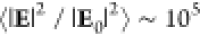 ), with an extremely narrow spectral width
(Δλ < 10 pm), can be obtained at an incidence angle
approaching the quasi-BIC condition (e.g., at θ = 0.1°)
in the nanopillar region corresponding to the emitting layer. Figure S6 of the Supporting Information shows
the simulated electric field enhancement in the nanoslot and the far-field
reflectance spectra for a plane wave impinging at θ = 0.1°
on the structure. The reflectance has the asymmetric Fano-like line-shape,
with its asymmetry parameter q → 0 at resonance.
In addition, Figure 2e shows that, as the incident radiation approaches the resonant condition
(i.e., θ = 0°), the line width of the mode becomes vanishingly
small, and accordingly its Q-factor increases enormously
(up to Q ∼ 1.5 × 10⁹, a value
limited by the numerical precision of the simulation). These features
are distinctive of quasi-BIC modes supported by arrays of all-dielectric
nanoresonators.24,26Figure S7 of the Supporting Information reports the influence of the
lattice parameter on the resonance Q-factor for the
sample with r = 360 nm. The highest Q-factor has been calculated for the configuration with the densest
array of nanopillars (i.e., a0 = 800 nm).
From the electric and magnetic near-field enhancement at λ =
1487 nm shown in Figure 2f, it can be noticed that the resonance has a quadrupole-like field
distribution, exhibiting four lobes where the electric or magnetic
field results strongly increased. Figure S8 of the Supporting Information shows y- and z-components of the electric and magnetic fields and the
vector field map at λ = 1487 nm.
), with an extremely narrow spectral width
(Δλ < 10 pm), can be obtained at an incidence angle
approaching the quasi-BIC condition (e.g., at θ = 0.1°)
in the nanopillar region corresponding to the emitting layer. Figure S6 of the Supporting Information shows
the simulated electric field enhancement in the nanoslot and the far-field
reflectance spectra for a plane wave impinging at θ = 0.1°
on the structure. The reflectance has the asymmetric Fano-like line-shape,
with its asymmetry parameter q → 0 at resonance.
In addition, Figure 2e shows that, as the incident radiation approaches the resonant condition
(i.e., θ = 0°), the line width of the mode becomes vanishingly
small, and accordingly its Q-factor increases enormously
(up to Q ∼ 1.5 × 10⁹, a value
limited by the numerical precision of the simulation). These features
are distinctive of quasi-BIC modes supported by arrays of all-dielectric
nanoresonators.24,26Figure S7 of the Supporting Information reports the influence of the
lattice parameter on the resonance Q-factor for the
sample with r = 360 nm. The highest Q-factor has been calculated for the configuration with the densest
array of nanopillars (i.e., a0 = 800 nm).
From the electric and magnetic near-field enhancement at λ =
1487 nm shown in Figure 2f, it can be noticed that the resonance has a quadrupole-like field
distribution, exhibiting four lobes where the electric or magnetic
field results strongly increased. Figure S8 of the Supporting Information shows y- and z-components of the electric and magnetic fields and the
vector field map at λ = 1487 nm.
As a reference, a similar array of Si nanopillars without the SiO2 slot was also simulated and a similar quadrupole quasi-BIC resonance (with Q ∼ 109) was found at a slightly longer wavelength (see Figure S9 in the Supporting Information). The x–z view in Figure S9 shows that the low index material of the slot (SiO2) increases the electric field enhancement in the emitting layer by roughly 3 times. Therefore, slotted Si nanopillars can be considered a significant advancement with respect to all-silicon nanopillars without the slot, since they preserve the activation of quasi-BIC modes with high Q-factors and, at the same time, they are able to tailor the emitter position in the region with the highest LDOS enhancement.
Figure 3a shows the measured Er3+ PL intensity enhancement with respect to a 30 nm thick planar Si slot for a selected set of samples with quasi-BIC resonances in the Er3+ wavelength emission range. The PL signal was collected normal to the surface of the sample with NA = 0.05. A PL enhancement of more than 1 order of magnitude was measured over the whole Er3+ emission spectrum. This confirms that the periodic nanopillar geometry strongly favors the out-coupling of the emitted radiation toward the far-field with respect to the planar film structure, as discussed in detail in ref (20). Furthermore, in correspondence to quasi-BIC resonances (labeled with capital letters from A to F in Figure 3) the Er3+ PL intensity is increased up to 3 orders of magnitude with respect to the planar configuration. This clearly shows that the photon emission from the nanoslot is strongly amplified when the coupling with quasi-BIC resonances is achieved. In the explored wavelength range, six eigenmodes with extremely high Q-factors (up to Q ∼ 109) have been found. The resonances with Q > 102 are reported in Figure 3b. The huge Q-factor exhibited by the eigenmodes computed in the slot nanoantennas is consistent with the excitation of optical quasi-BICs.15,24,26 The spectral position of the eigenmodes is in good agreement with the sharp peaks measured in the PL spectra. Considering the electric and magnetic field configuration at the resonances (see Figure 3c), it emerges that the resonance labeled with A and F are toroidal dipole (TD) BIC eigenmodes with dominant ED and MD moment,24,50 respectively, while B, D, and E present the characteristic quadrupole-like electromagnetic near-field distribution. The C mode is a broader Mie-type magnetic dipole resonance15 with a relatively modest Q-factor (Q < 102) and correspondingly a lower PL enhancement is obtained (see Figure 3a).
Figure 3.

(a) Measured Er3+ PL intensity enhancement in logarithmic scale in the 1450–1630 nm wavelength range with respect to a 30 nm thick planar nanoslot. (b) Q-factor for the eigenmodes computed by the modal analysis. (c) Electric and magnetic field distribution in the SiO2 slot for the modes calculated by the modal analysis. The electromagnetic field distribution of the B resonance is shown in Figure 2e.
It is worth saying that a Q-factor of Q ∼ 106 in the 1450–1650 nm wavelength range corresponds to an ultranarrow resonance line width Δλ ∼ 10–3 nm, which is extremely challenging to be measured from the experimental point of view. Moreover, quasi-BIC resonances are extremely narrow also from an angular point of view considering the emission directivity (e.g., see Figure 2e). Hence, we expect that the monochromator resolution (Δλmin ∼ 2 nm), the numerical aperture of the collection lens (NA = 0.05) largely contribute to broaden the width of the measured resonances.47 In addition, the average random emitter orientation in the SiO2 nanoslot decreases the number of erbium ions able to efficiently couple with these highly directional modes and reduces the measured intensity of the resonance. Finally, since mathematical quasi-BIC consist of infinite arrays of identical nanostructures, the finite size effect of the periodic arrays51 and nanofabrication imperfections52 can decrease significantly the measured Q-factor. Since the fabricated nanopillar arrays are 400 × 400 μm large (i.e., containing more than 105 nanoantennas), a marginal effect is expected in the Q-factor of the quasi-BIC modes due to the finite size of the structure.48,51Figure S10 of the Supporting Information shows the effect of a distribution of nanoparticles radii on the resonance Q-factor for the sample with r = 360 nm and a0 = 800 nm, suggesting that nanofabrication imperfections can contribute to limit the maximum Q-factor achievable experimentally. Despite all these limiting effects, it is worth highlighting that we have measured a boost of the Er3+ photon emission (at telecom wavelength) by almost 3 orders of magnitude at room temperature in a relatively simple photonic geometry that does not need too complex nanofabrication processes.
Finally, we have designed the nanoantennas array emission directivity. We have exploited the coupling of Er3+ emission with quasi-BIC modes to tailor the angular distribution of the PL emission, obtaining a strong beaming effect. To calculate the angular distribution of the Er3+ PL emission, the approach based on the reciprocity principle has been adopted. Since the Er3+ PL signal was collected along the Γ–X direction of the first Brillouin zone in the reciprocal lattice, keeping constant the azimuthal angle (ϕ = 0 in the present case), the PL intensity as a function of the emission wavelength and the polar angle (θ) can be estimated as53−55
| 1 |
with:
where K is a constant that accounts for the collection efficiency of the experimental setup, E(r; λ, θ) and H(r; λ, θ) are the FEM simulated electric and magnetic local field for TE- and TM-polarized plane waves impinging on the nanostructure from the air half-space, ⟨ · ⟩ denotes the volume average inside the emitting layer (i.e., the Er:SiO2 slot), and IED(λ) and IMD(λ) are the Er3+ PL emission intensities in SiO2 for the limiting cases of ηED = 1 and ηMD = 1, respectively. Using eq 1, the PL intensity distribution maps have been estimated and are reported in Figure 4a–c for the set of samples with r = 220, 360, and 390 nm. Figure 4d–f show the corresponding measured angular distribution of the Er3+ PL intensity in the 1400–1650 nm wavelength range. The line-shape of the Er3+ PL intensity in the 1400–1650 nm wavelength range is significantly altered by the branching ratio. Figure S11 shows the limiting cases for ηED = 1 and ηMD = 1, calculated from a set of samples with the Er:SiO2 emitting layer placed at different distances from a gold mirror.42,45 The PL maps present maxima of the emission intensity in correspondence to specific (θ, λ) configurations, where the emitted light couples to modes supported by the nanopillar array. For example, it is worth noticing that the sample with r = 220 nm and a0 = 1000 nm shows a PL maximum at λ = 1540 nm for a collection angle close to the normal to the sample surface (see Figure 4g), and about 90% of the emitted radiation is focused in a Δθ ∼ ±10° lobe normal to the sample surface where the Er3+ PL couples with the toroidal dipole BIC resonance (i.e., resonance labeled with A in Figure 3). This proves that not only decay rate enhancements, but also strong beaming effects can be achieved when the coupling of Er3+ luminescence with high-Q modes is carefully designed. Our findings demonstrate that slotted nanopillars are highly promising candidates for the development of more efficient or novel light sources. For example, by decreasing the emitter concentration by roughly 2 orders of magnitude, bright, lossless, and highly directional single-photon sources operating at telecom wavelength could be realized.
Figure 4.

Emission directivity. PL intensity distribution calculated by eq 1 for slotted nanopillars with (a) r = 220, (b) 360, and (c) 390 nm. (d–f) Measured angular distribution in the 1400–1650 nm wavelength range for the corresponding samples. (g) Measured angular distribution of the Er3+ PL intensity at λ = 1540 nm for the sample with r = 220 nm and a0 = 1000 nm.
Conclusion
We have designed and realized all-dielectric lossless nanoantennas able to boost the Er3+ photon emission in the telecom wavelength band and at room temperature. We have shown that ultrahigh Q-factor resonances (Q > 105) are supported by square arrays of silicon nanopillars with a 30 nm thick Erbium-doped SiO2 slot placed at half of the nanopillar height. The eigenvalue analysis performed by FEM simulations evidenced electric and magnetic dipole and quadrupole quasi-BIC modes. These modes are characterized by a giant local density of optical states enhancement inside the nanopillars and specifically in the region corresponding to the optically active layer. Two orders of magnitude decay rate enhancement and almost 3 orders of magnitude PL intensity increment have been measured at room temperature for the Er3+ radiative emission in the range λ = 1400–1650 nm when the coupling with quasi-BIC resonances is achieved. Furthermore, we have demonstrated that the slot geometry can be exploited to obtain selective emission enhancements for Er3+ electric and magnetic radiative transitions at λ = 1540 nm and that by tailoring the nanopillar aspect ratio from AR ∼ 0.5 to AR ∼ 2 the emitter magnetic branching ratio can be varied from ηMD = 0.18 to 0.85, keeping the quantum efficiency almost unitary. Finally, by computing the angularly resolved electromagnetic field enhancement inside the nanoslot it was possible to predict and control the emission directivity of the nanoantenna, focusing more than 90% of the emitted radiation in a lobe normal to the sample surface when the coupling with quasi-BIC resonances is achieved.
Methods
Sample Preparation
A sketch of the sample structure is shown in Figure 1a. To realize the slotted nanopillars (Figure 1a), as the first step silicon thin films (200 ± 10 nm thick) were deposited by magnetron sputtering on a silica slab (Herasil, by Heraeus). A 2″ diameter Si target was mounted on a DC source and the deposition was performed at a power P = 100 W and a pressure p = 5 × 10⁻³ mbar. Before the deposition, the silica substrates were cleaned in a “piranha” solution (3:1, H2SO4/H2O2) for 1 h and rinsed in ultrapure water. Erbium-doped silica (Er:SiO2) thin films (30 ± 1 nm thick) were also deposited by means of magnetron cosputtering. A metallic erbium target (diameter 2″, thickness 1/4″, purity 99.99%, by K. J. Lesker) was mounted on the DC source, while a silicon dioxide target (diameter 2″, thickness 1/8″, purity 99.9%, by K. J. Lesker) was placed on a radiofrequency (RF) source. The depositions were performed in a slightly oxidizing atmosphere (95% Ar + 5% O2) in order to obtain stoichiometric SiO2 layers.56 Both sources were tilted of about 25° to aim at the center of the sample holder, which was kept under rotation to ensure homogeneity of the deposited films. The power of the two sources was set to keep the Er concentration at 0.3 at. % below the concentration quenching limit ([Er]<1 at. %). Rutherford backscattering spectrometry (RBS) was used to confirm the Er concentration and to exclude the presence of contaminants in the Er:SiO2 layer. Thickness and roughness of the deposited films were determined by atomic force microscopy (AFM) measurements with a NT-MDT Solver-Pro AFM in noncontact mode. The dielectric functions were determined by means of a Woollam variable angle spectroscopic ellipsometer (VASE).
After the deposition of Si/Er:SiO2/Si multilayers on silica substrates, the samples were further cleaned in a “piranha” solution and annealed at 850 °C for 2 h in vacuum (p ∼ 5 × 10⁻⁵ mbar) to promote silicon densification and crystallization and to activate the Er3+ luminescence.
Then, an area of 400 × 400 μm2 was patterned with a square array of nanopillars by means of electron beam lithography (EBL) and reactive ion etching (RIE). Two sets of samples with square lattice parameters a0 = 800 and 1000 nm were fabricated. The pillar radius was varied from r = 125 to 390 nm, while the pillar height (h) was kept at h = 430 ± 10 nm.
FEM Simulations
FEM simulations were carried out in the frequency domain using the commercial software COMSOL Multiphysics and with EMUstack.57 Due to the difficulties associated with the simulation of a single emitter in periodic structures, two different computational approaches were exploited. To calculate the radiative decay rate variation at λem = 1540 nm, the Er3+ emitters were modeled as electric or magnetic dipoles,43 oscillating at the frequency corresponding to their emission. Each configuration was modeled with a single emitter placed at a specific position in the simulation domain and with a given orientation. To evaluate the finite-size effect on the Purcell factor, i.e., the influence of the neighboring nanostructures on the decay rate modification, configurations with 1, 9, 25, and 49 nanopillars in the simulation domain were considered (as discussed in the Supporting Information). The dipoles were oriented along the x-, y-, and z-axis. The isotropic orientation was calculated averaging with equal weight over the three orientations. To compare with the experimental measurements the electric and magnetic dipole results were averaged with a 50:50 weight, considered the 50:50 nature of the Er3+ emission at 1540 nm.58 Moreover, the approach based on the optical reciprocity principle45,55 was used to study the Er3+ emitters coupling with modes that require periodic structures (e.g., quasi-BICs). The modal analysis (computed by the eigenfrequency solver implemented in the commercial software COMSOL Multiphysics) and the electromagnetic field enhancement calculations in the slot were carried out with a square unit cell containing a single slotted nanopillar and applying periodic boundary conditions in the x–z and y–z planes and perfectly matching layers along the z-direction.
PL Measurements
PL measurements were performed using as the excitation source a cw fiber-coupled laser diode (λex = 520 nm, P = 50 mW) mechanically chopped at f = 20 Hz. Two different optical set-ups were used to collect the Er3+ radiative emission corresponding to the 4I13/2 →4I15/2 transition. Time-resolved photoluminescence measurements at λ = 1540 nm (Figure 1b) were taken in a confocal configuration using an objective with numerical aperture NA = 0.85 to maximize the signal-to-noise ratio and the acceptance angle. For the angle resolved PL measurements, the laser diode was mounted on a rotating stage, allowing for the collection of the emitted radiation from θ = 0° to ±90° without altering the angle of incidence between the pumping beam and the sample surface (θinc = 30°). The PL emission was collected with a converging lens (focal length f = 10 cm). An iris was used to vary the numerical aperture of the collecting system in the range NA = 0.05–0.2. The collected PL signal was focused on the entrance slit of a single grating monochromator coupled with a N2-cooled photomultiplier tube (HAMAMATSU R5509-72).
Acknowledgments
The financial support of the Physics and Astronomy Department with the project PRD-BIRD2022-Cesca is gratefully acknowledged. R.S. acknowledges funding by the Engineering and Physical Sciences Research Council (EPSRC) (grant no. EP/V048880). S.A.M. acknowledges the EPSRC (EP/W017075/1) and the Lee-Lucas Chair in Physics.
Supporting Information Available
The Supporting Information is available free of charge at https://pubs.acs.org/doi/10.1021/acsphotonics.2c01703.
Simulated and measured transmittance spectra at normal incidence, measured Si dielectric function, the variation of the Purcell factor with respect to the electric and magnetic dipole position inside the nanoslot, the radiative decay rate modification as a function of the number of nanopillars in the simulated domain, field intensity maps in the SiO2 slot, the influence of the numerical aperture of the collection lens and of the monochromator slits width on the PL spectrum, simulated field intensity and reflectance spectra for the sample with r = 360 nm and a0 = 800 nm, the influence of the lattice parameter on the Q-factor, near-field maps for the resonance with Q ∼ 109, the influence of nanofabrication imperfections on the Q-factor, the field distribution in the nanopillar with and without the slot, and Er3+ ED and MD PL intensity spectra (PDF)
The authors declare no competing financial interest.
Supplementary Material
References
- Novotny L.; Hecht B.. Principles of Nano-Optics; Cambridge University Press, 2012. [Google Scholar]
- Purcell E. M.; Torrey H. C.; Pound R. V. Resonance absorption by nuclear magnetic moments in a solid. Phys. Rev. 1946, 69, 37. 10.1103/PhysRev.69.37. [DOI] [Google Scholar]
- Drexhage K. Influence of a dielectric interface on fluorescence decay time. Journal of luminescence 1970, 1, 693–701. 10.1016/0022-2313(70)90082-7. [DOI] [Google Scholar]
- Giannini V.; Fernández-Domínguez A. I.; Heck S. C.; Maier S. A. Plasmonic nanoantennas: fundamentals and their use in controlling the radiative properties of nanoemitters. Chem. Rev. 2011, 111, 3888–3912. 10.1021/cr1002672. [DOI] [PubMed] [Google Scholar]
- Akselrod G. M.; Argyropoulos C.; Hoang T. B.; Ciracì C.; Fang C.; Huang J.; Smith D. R.; Mikkelsen M. H. Probing the mechanisms of large Purcell enhancement in plasmonic nanoantennas. Nat. Photonics 2014, 8, 835. 10.1038/nphoton.2014.228. [DOI] [Google Scholar]
- Cesca T.; Michieli N.; Kalinic B.; Balasa I. G.; Rangel-Rojo R.; Reyes-Esqueda J. A.; Mattei G. Bidimensional ordered plasmonic nanoarrays for nonlinear optics, nanophotonics and biosensing applications. Materials Science in Semiconductor Processing 2019, 92, 2–9. 10.1016/j.mssp.2018.03.025. [DOI] [Google Scholar]
- Michieli N.; Kalinic B.; Scian C.; Cesca T.; Mattei G. Emission rate modification and quantum efficiency enhancement of Er3+ emitters by near-field coupling with nanohole arrays. ACS Photonics 2018, 5, 2189–2199. 10.1021/acsphotonics.8b00042. [DOI] [Google Scholar]
- Castanié E.; Boffety M.; Carminati R. Fluorescence quenching by a metal nanoparticle in the extreme near-field regime. Opt. Lett. 2010, 35, 291–293. 10.1364/OL.35.000291. [DOI] [PubMed] [Google Scholar]
- Gonçalves P. A.; Christensen T.; Rivera N.; Jauho A. P.; Mortensen N. A.; Soljačić M. Plasmon–emitter interactions at the nanoscale. Nat. Commun. 2020, 11, na. 10.1038/s41467-019-13820-z. [DOI] [PMC free article] [PubMed] [Google Scholar]
- Anger P.; Bharadwaj P.; Novotny L. Enhancement and quenching of single-molecule fluorescence. Phys. Rev. Lett. 2006, 96, 113002. 10.1103/PhysRevLett.96.113002. [DOI] [PubMed] [Google Scholar]
- Kühn S.; Håkanson U.; Rogobete L.; Sandoghdar V. Enhancement of single-molecule fluorescence using a gold nanoparticle as an optical nanoantenna. Physical review letters 2006, 97, 017402. 10.1103/PhysRevLett.97.017402. [DOI] [PubMed] [Google Scholar]
- Aharonovich I.; Englund D.; Toth M. Solid-state single-photon emitters. Nat. Photonics 2016, 10, 631–641. 10.1038/nphoton.2016.186. [DOI] [Google Scholar]
- Kuznetsov A. I.; Miroshnichenko A. E.; Fu Y. H.; Zhang J.; Lukyanchuk B. Magnetic light. Sci. Rep. 2012, 2, 1–6. 10.1038/srep00492. [DOI] [PMC free article] [PubMed] [Google Scholar]
- Kruk S.; Kivshar Y. Functional Meta-Optics and Nanophotonics Govern by Mie Resonances. ACS Photonics 2017, 4, 2638–2649. 10.1021/acsphotonics.7b01038. [DOI] [Google Scholar]
- Koshelev K.; Kivshar Y. Dielectric Resonant Metaphotonics. ACS Photonics 2021, 8, 102–112. 10.1021/acsphotonics.0c01315. [DOI] [Google Scholar]
- Liu T.; Xu R.; Yu P.; Wang Z.; Takahara J. Multipole and multimode engineering in Mie resonance-based metastructures. Nanophotonics 2020, 9, 1115–1137. 10.1515/nanoph-2019-0505. [DOI] [Google Scholar]
- Krasnok A. E.; Miroshnichenko A. E.; Belov P. A.; Kivshar Y. S. All-dielectric optical nanoantennas. Opt. Express 2012, 20, 20599–20604. 10.1364/OE.20.020599. [DOI] [PubMed] [Google Scholar]
- Mignuzzi S.; Vezzoli S.; Horsley S. A.; Barnes W. L.; Maier S. A.; Sapienza R. Nanoscale Design of the Local Density of Optical States. Nano Lett. 2019, 19, 1613–1617. 10.1021/acs.nanolett.8b04515. [DOI] [PubMed] [Google Scholar]
- Vaskin A.; Bohn J.; Chong K. E.; Bucher T.; Zilk M.; Choi D. Y.; Neshev D. N.; Kivshar Y. S.; Pertsch T.; Staude I. Directional and Spectral Shaping of Light Emission with Mie-Resonant Silicon Nanoantenna Arrays. ACS Photonics 2018, 5, 1359–1364. 10.1021/acsphotonics.7b01375. [DOI] [Google Scholar]
- Kalinic B.; Cesca T.; Mignuzzi S.; Jacassi A.; Balasa I. G.; Maier S. A.; Sapienza R.; Mattei G. All-Dielectric Silicon Nanoslots for Er3+ Photoluminescence Enhancement. Physical Review Applied 2020, 14, 014086. 10.1103/PhysRevApplied.14.014086. [DOI] [Google Scholar]
- Sortino L.; Zotev P. G.; Mignuzzi S.; Cambiasso J.; Schmidt D.; Genco A.; Aßmann M.; Bayer M.; Maier S. A.; Sapienza R.; Tartakovskii A. I. Enhanced light–matter interaction in an atomically thin semiconductor coupled with dielectric nano-antennas. Nat. Commun. 2019, 10, 1–8. 10.1038/s41467-019-12963-3. [DOI] [PMC free article] [PubMed] [Google Scholar]
- Zambrana-Puyalto X.; Bonod N. Purcell factor of spherical Mie resonators. Phys. Rev. B 2015, 91, 195422. 10.1103/PhysRevB.91.195422. [DOI] [Google Scholar]
- Kuznetsov A. I.; Miroshnichenko A. E.; Brongersma M. L.; Kivshar Y. S.; Luk’yanchuk B. Optically resonant dielectric nanostructures. Science 2016, 354, na. 10.1126/science.aag2472. [DOI] [PubMed] [Google Scholar]
- He Y.; Guo G.; Feng T.; Xu Y.; Miroshnichenko A. E. Toroidal dipole bound states in the continuum. Phys. Rev. B 2018, 98, na. 10.1103/PhysRevB.98.161112. [DOI] [Google Scholar]
- Hsu C. W.; Zhen B.; Stone A. D.; Joannopoulos J. D.; Soljacic M. Bound states in the continuum. Nature Reviews Materials 2016, 1, na. 10.1038/natrevmats.2016.48. [DOI] [Google Scholar]
- Bogdanov A. A.; Koshelev K. L.; Kapitanova P. V.; Rybin M. V.; Gladyshev S. A.; Sadrieva Z. F.; Samusev K. B.; Kivshar Y. S.; Limonov M. F. Bound states in the continuum and Fano resonances in the strong mode coupling regime. Advanced Photonics 2019, 1, 1. 10.1117/1.AP.1.1.016001. [DOI] [Google Scholar]
- Rybin M. V.; Koshelev K. L.; Sadrieva Z. F.; Samusev K. B.; Bogdanov A. A.; Limonov M. F.; Kivshar Y. S. High- Q Supercavity Modes in Subwavelength Dielectric Resonators. Phys. Rev. Lett. 2017, 119, 1–5. 10.1103/PhysRevLett.119.243901. [DOI] [PubMed] [Google Scholar]
- Azzam S. I.; Kildishev A. V. Photonic Bound States in the Continuum: From Basics to Applications. Advanced Optical Materials 2021, 9, 16–24. 10.1002/adom.202001469. [DOI] [Google Scholar]
- Koshelev K.; Kruk S.; Melik-Gaykazyan E.; Choi J.-H.; Bogdanov A.; Park H.-G.; Kivshar Y. Subwavelength dielectric resonators for nonlinear nanophotonics. Science 2020, 367, 288–292. 10.1126/science.aaz3985. [DOI] [PubMed] [Google Scholar]
- Tiguntseva E.; Koshelev K.; Furasova A.; Tonkaev P.; Mikhailovskii V.; Ushakova E. V.; Baranov D. G.; Shegai T.; Zakhidov A. A.; Kivshar Y.; et al. Room-temperature lasing from Mie-resonant nonplasmonic nanoparticles. ACS Nano 2020, 14, 8149–8156. 10.1021/acsnano.0c01468. [DOI] [PubMed] [Google Scholar]
- Yu Y.; Sakanas A.; Zali A. R.; Semenova E.; Yvind K.; Mørk J. Ultra-coherent Fano laser based on a bound state in the continuum. Nat. Photonics 2021, 15, 758–764. 10.1038/s41566-021-00860-5. [DOI] [Google Scholar]
- Xu H.; Shi Y. Silicon-Waveguide-Integrated High-Quality Metagrating Supporting Bound State in the Continuum. Laser & Photonics Reviews 2020, 14, 1900430. 10.1002/lpor.201900430. [DOI] [Google Scholar]
- Yesilkoy F.; Arvelo E. R.; Jahani Y.; Liu M.; Tittl A.; Cevher V.; Kivshar Y.; Altug H. Ultrasensitive hyperspectral imaging and biodetection enabled by dielectric metasurfaces. Nat. Photonics 2019, 13, 390–396. 10.1038/s41566-019-0394-6. [DOI] [Google Scholar]
- Doeleman H. M.; Monticone F.; den Hollander W.; Alù A.; Koenderink A. F. Experimental observation of a polarization vortex at an optical bound state in the continuum. Nat. Photonics 2018, 12, 397–401. 10.1038/s41566-018-0177-5. [DOI] [Google Scholar]
- Bharadwaj P.; Deutsch B.; Novotny L. Optical antennas. Advances in Optics and Photonics 2009, 1, 438–483. 10.1364/AOP.1.000438. [DOI] [Google Scholar]
- Koenderink A. F. Single-photon nanoantennas. ACS Photonics 2017, 4, 710–722. 10.1021/acsphotonics.7b00061. [DOI] [PMC free article] [PubMed] [Google Scholar]
- Almeida V. R.; Xu Q.; Barrios C. A.; Lipson M. Guiding and confining light in void nanostructure. Optics letters 2004, 29, 1209–1211. 10.1364/OL.29.001209. [DOI] [PubMed] [Google Scholar]
- Galli M.; Gerace D.; Politi A.; Liscidini M.; Patrini M.; Andreani L. C.; Canino A.; Miritello M.; Savio R. L.; Irrera A.; et al. Direct evidence of light confinement and emission enhancement in active silicon-on-insulator slot waveguides. Appl. Phys. Lett. 2006, 89, 241114. 10.1063/1.2404936. [DOI] [Google Scholar]
- Agio M.; Alù A.. Optical Antennas; Cambridge University Press, 2013. [Google Scholar]
- Dibos A.; Raha M.; Phenicie C.; Thompson J. D. Atomic source of single photons in the telecom band. Phys. Rev. Lett. 2018, 120, 243601. 10.1103/PhysRevLett.120.243601. [DOI] [PubMed] [Google Scholar]
- Polman A. Erbium implanted thin film photonic materials. Journal of applied physics 1997, 82, 1–39. 10.1063/1.366265. [DOI] [Google Scholar]
- Li D.; Jiang M.; Cueff S.; Dodson C. M.; Karaveli S.; Zia R. Quantifying and controlling the magnetic dipole contribution to 1.5-μm light emission in erbium-doped yttrium oxide. Phys. Rev. B 2014, 89, 161409. 10.1103/PhysRevB.89.161409. [DOI] [Google Scholar]
- Li D.; Karaveli S.; Cueff S.; Li W.; Zia R. Probing the combined electromagnetic local density of optical states with quantum emitters supporting strong electric and magnetic transitions. Phys. Rev. Lett. 2018, 121, 227403. 10.1103/PhysRevLett.121.227403. [DOI] [PubMed] [Google Scholar]
- Vaskin A.; et al. Manipulation of magnetic dipole emission from Eu3+ with Mie-resonant dielectric metasurfaces. Nano Lett. 2019, 19, 1015–1022. 10.1021/acs.nanolett.8b04268. [DOI] [PubMed] [Google Scholar]
- Choi B.; Iwanaga M.; Sugimoto Y.; Sakoda K.; Miyazaki H. T. Selective plasmonic enhancement of electric-and magnetic-dipole radiations of Er ions. Nano Lett. 2016, 16, 5191–5196. 10.1021/acs.nanolett.6b02200. [DOI] [PubMed] [Google Scholar]
- Kalinic B.; Cesca T.; Scian C.; Michieli N.; Balasa I. G.; Trave E.; Mattei G. Emission Efficiency Enhancement of Er3+ Ions in Silica by Near-Field Coupling With Plasmonic and Pre-Plasmonic Nanostructures. Physica Status Solidi (a) 2018, 215, 1700437. 10.1002/pssa.201700437. [DOI] [Google Scholar]
- Liang Y.; Lin H.; Lin S.; Wu J.; Li W.; Meng F.; Yang Y.; Huang X.; Jia B.; Kivshar Y. Hybrid anisotropic plasmonic metasurfaces with multiple resonances of focused light beams. Nano Lett. 2021, 21, 8917–8923. 10.1021/acs.nanolett.1c02751. [DOI] [PubMed] [Google Scholar]
- Zundel L.; Deop-Ruano J. R.; Martinez-Herrero R.; Manjavacas A. Lattice Resonances Excited by Finite-Width Light Beams. ACS omega 2022, 7, 31431–31441. 10.1021/acsomega.2c03847. [DOI] [PMC free article] [PubMed] [Google Scholar]
- Cesca T.; Maurizio C.; Kalinic B.; Perotto G.; Mazzoldi P.; Trave E.; Battaglin G.; Mattei G. Implantation damage effects on the Er3+ luminescence in silica. Opt. Express 2012, 20, 16639–16649. 10.1364/OE.20.016639. [DOI] [Google Scholar]
- Papasimakis N.; Fedotov V.; Savinov V.; Raybould T.; Zheludev N. Electromagnetic toroidal excitations in matter and free space. Nature materials 2016, 15, 263–271. 10.1038/nmat4563. [DOI] [PubMed] [Google Scholar]
- Liu Z.; Xu Y.; Lin Y.; Xiang J.; Feng T.; Cao Q.; Li J.; Lan S.; Liu J. High-Q quasibound states in the continuum for nonlinear metasurfaces. Physical review letters 2019, 123, 253901. 10.1103/PhysRevLett.123.253901. [DOI] [PubMed] [Google Scholar]
- Kühne J.; Wang J.; Weber T.; Kühner L.; Maier S. A.; Tittl A. Fabrication robustness in BIC metasurfaces. Nanophotonics 2021, 10, 4305–4312. 10.1515/nanoph-2021-0391. [DOI] [Google Scholar]
- Zschiedrich L.; Greiner H. J.; Burger S.; Schmidt F. Numerical analysis of nanostructures for enhanced light extraction from OLEDs. Light-Emitting Diodes: Materials, Devices, and Applications for Solid State Lighting XVII.. Proc. SPIE 2013, 8641, 86410B. 10.1117/12.2001132. [DOI] [Google Scholar]
- Zhang S.; Martins E. R.; Diyaf A. G.; Wilson J. I.; Turnbull G. A.; Samuel I. D. Calculation of the emission power distribution of microstructured OLEDs using the reciprocity theorem. Synth. Met. 2015, 205, 127–133. 10.1016/j.synthmet.2015.03.035. [DOI] [Google Scholar]
- Vaskin A.; et al. Manipulation of Magnetic Dipole Emission from Eu3+ with Mie-Resonant Dielectric Metasurfaces. Nano Lett. 2019, 19, 1015–1022. 10.1021/acs.nanolett.8b04268. [DOI] [PubMed] [Google Scholar]
- Kalinic B.; Cesca T.; Michieli N.; Scian C.; Battaglin G.; Mazzoldi P.; Mattei G. Controlling the emission rate of Er3+ ions by dielectric coupling with thin films. J. Phys. Chem. C 2015, 119, 6728–6736. 10.1021/jp510239d. [DOI] [Google Scholar]
- Sturmberg B. C.; Dossou K. B.; Lawrence F. J.; Poulton C. G.; McPhedran R. C.; De Sterke C. M.; Botten L. C. EMUstack: an open source route to insightful electromagnetic computation via the Bloch mode scattering matrix method. Comput. Phys. Commun. 2016, 202, 276–286. 10.1016/j.cpc.2015.12.022. [DOI] [Google Scholar]
- Liu W.; Shi J.; Lei B.; Hu H.; Miroshnichenko A. E. Efficient excitation and tuning of toroidal dipoles within individual homogenous nanoparticles. Opt. Express 2015, 23, 24738. 10.1364/OE.23.024738. [DOI] [PubMed] [Google Scholar]
Associated Data
This section collects any data citations, data availability statements, or supplementary materials included in this article.