Abstract
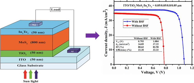
Researchers are currently showing interest in molybdenum disulfide (MoS2)-based solar cells due to their remarkable semiconducting characteristics. The incompatibility of the band structures at the BSF/absorber and absorber/buffer interfaces, as well as carrier recombination at the rear and front metal contacts, prevents the expected result from being achieved. The main purpose of this work is to enhance the performance of the newly proposed Al/ITO/TiO2/MoS2/In2Te3/Ni solar cell and investigate the impacts of the In2Te3 BSF and TiO2 buffer layer on the performance parameters of open-circuit voltage (VOC), short-circuit current density (JSC), fill factor (FF), and power conversion efficiency (PCE). This research has been performed by utilizing SCAPS simulation software. The performance parameters such as variation of thickness, carrier concentration, the bulk defect concentration of each layer, interface defect, operating temperature, capacitance–voltage (C–V), surface recombination velocity, and front as well as rear electrodes have been analyzed to achieve a better performance. This device performs exceptionally well at lower carrier concentrations (1 × 1016 cm–3) in a thin (800 nm) MoS2 absorber layer. The PCE, VOC, JSC, and FF values of the Al/ITO/TiO2/MoS2/Ni reference cell have been estimated to be 22.30%, 0.793 V, 30.89 mA/cm2, and 80.62% respectively, while the PCE, VOC, JSC, and FF values have been determined to be 33.32%, 1.084 V, 37.22 mA/cm2, and 82.58% for the Al/ITO/TiO2/MoS2/In2Te3/Ni proposed solar cell by introducing In2Te3 between the absorber (MoS2) and the rear electrode (Ni). The proposed research may give an insight and a feasible way to realize a cost-effective MoS2-based thin-film solar cell.
1. Introduction
Energy consumption and utilization have been rising with the rapid technological advancement, overpopulation, and the progression of impoverished areas around the world. Energy consumption in 2050 is expected to reach 30 terawatts (TW).1,2 To meet the current and future global electricity demands, the manufacture of solar cells has expanded dramatically in recent years. Approximately 90% of the present photovoltaic cell market is silicon (Si)-based.3,4 Si-based solar cells have a variety of drawbacks, including cost, weather dependence, space requirements, pollution concerns, rigidity, and high production costs.5,6 Due to their cheap manufacturing costs, established fabrication technologies, large-scale production flexibility, and extremely effective power conversion, thin-film solar cells (TFSCs) are becoming more attractive in photovoltaic (PV) technology.7−9 To produce cheaper, greater-efficiency, and greener solar cells, researchers in this field explore some criteria such as earth-abundant and nontoxic materials.
The three most popular thin film solar cells on the market are a-Si, CdTe, and CIGS. Various a-Si-, CdTe-, and CIGS-based TFSC structures have been developed practically and numerically to improve the performance of PV cells.10−12 The highest practical efficiency of α-Si, CdTe, and CIGS has been recorded at 13.6, 22.3, and 22.1%, respectively.13 Copper zinc tin sulfide (CZTS) is an earth-abundant solar cell material and a replacement for CIGS.14 The highest theoretical efficiency has been recorded at 30.79%.15
Recently, transition metal dichalcogenides (TMDs) have been getting attraction due to their remarkable optical and electrical features such as tunable bandgap, large absorption coefficient, and suitable transportation of electrons.16−18 TMD compounds having monolayer structures, for example, MX2, where M, transition metal atom (Mo, W, Nb, Ti), and X, Chalcogen atom, (S, Se, Te) have gained popularity for their use in PV cells.19,20 Furthermore, 2D materials with distinct crystal structures may help build a strong hetero-junction with excellent interfacial properties that are not affected by lattice mismatch.21 The bandgap of molybdenum disulfide (MoS2) varies from indirect to direct, increasing from 1.2 to 1.8 eV, indicating that the bandgap of MoS2 is flexible as well as has multiple benefits in optoelectronics.22 MoS2 has an absorption coefficient of around 2.8 × 106 cm–1 with a statistical uncertainty of ±1.3 × 105 cm–1.23 Due to these promising properties, several PV cell structures of MoS2-based solar cells have been constructed and analyzed experimentally24−27 and analytically28,29 in earlier research to attain better performance.
The experimental power conversion efficiency (PCE) of the MoS2-based Schottky-barrier solar cell (ITO/MoS2/Au) was only 0.7 and 1.8% for the thickness of 110 and 220 nm absorber layer, respectively.24 The same group also constructed an ITO/TiO2/MoS2/P3HT/Au structure with a PCE of 1.3%.25 The PCE of 5.23% has been achieved in a hetero-structure PV cell composed of n-MoS2 (monolayer)/p-Si.27 The experimental PCE of a 2-D WSe2/MoS2 p–n hetero-structure-based transpicuous SC has reached ∼10%.26 A PV cell structure of ZnO/CdS/MoS2 has exhibited a PCE of 19.62%, suggesting MoS2 as a suitable absorber layer for solar cells.28 The theoretical maximum efficiency of optimized ITO/ZnSe/MoS2 and ITO/ZnSe/MoS2/SnS photovoltaic cells has been observed as 19.48 and 21.39%, respectively.29
The present determined performance parameters VOC, JSC, fill factor (FF), and PCE of the MoS2 SC are not able to compete with other heterojunction TFSCs. The carrier recombination at the junction may reduce VOC and JSC. Moreover, the inadequate carrier transportation, accumulation at the electrodes, and carrier recombination at the junction due to the absence of back surface field (BSF) or HTL and buffer layer cause the reduction of the VOC and JSC, which results in degradation of conversion efficiency.30,31 The conventional MoS2 SCs need to be remodeled for achieving better performance by inserting a suitable buffer and BSF between the absorber layer and rear electrode. The buffer layer in the SC is positioned between the window and absorber, which together form a p–n junction. It eliminates defects as well as interfacial strain caused by the window layer.32 Therefore, it is crucial to continue further research work to attain enhanced performance of the TFSCs based on the MoS2 absorber layer. The redesigning of the MoS2 SC with a suitable BSF or buffer layer is very much essential. The BSF layer with desirable physical, optical, and chemical stability will facilitate proper transportation and accumulation of photogenerated carriers (PGCs) from the absorber layer to the metal electrodes. In this case, rather than using a CdS or ZnSe buffer layer, we consider using an n-type TiO2 layer for MoS2-based TFSCs to get better performance. It is an inert, nontoxic, and safe substance with exceptional better performance. The BSF layer has been developed in this study with 50 nm-thick indium telluride (In2Te3) in the molybdenum disulfide (MoS2) solar cell, because of its ability to accumulate holes more effectively as well as reduces electron–hole recombination. Furthermore, the placement of BSF between the absorber and rear electrode can minimize the absorber layer thickness, minimizing the PV cell’s overall cost.33,34
In this article, the photovoltaic performance parameters of the proposed (ITO/TiO2/MoS2/In2Te3) MoS2-based thin-film heterojunction SC without and with BSF have been analyzed utilizing the SCAPS-1D simulator. The investigation of the influence of the thickness, carrier concentration, defect density, working temperature, band alignment, rear electrode, capacitance–voltage (C–V), and back surface recombination velocity (SRV) on SC output parameters has been performed for optimizing the device structure as well as to determine better photoconversion efficiency in a cost-effective way.
2. Device Construction and Simulation Methodology
To explore the newly constructed ITO/TiO2/MoS2/In2Te3 photovoltaic cell, the one-dimensional Solar Cell Capacitance Simulator (SCAPS) application has been used for simulation purposes. Promising software named SCAPS-1D was developed at the Electronic and Information Systems Department of the University of Ghent, Belgium. It may be used to predict as well as examine the optoelectronic characteristics of PV cell structures by solving fundamental equations such as electrostatic potential and continuity equation under steady-state conditions.35 Up to seven semiconductor material layers in a solar cell may be examined in the most recent version, SCAPS 3.8, which was released in May 2020.
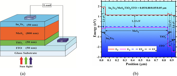
Figure 1a illustrates the heterojunction TFSC structure of the Al/ITO/TiO2/MoS2/In2Te3/Ni. The p-type MoS2 absorber layer is sandwiched between the highly doped p+-type In2Te3 BSF and n-type TiO2 buffer layer to form a p+–p–n–n+ structure. A p-type absorber layer, highly doped p+-type In2Te3 BSF, n-type TiO2 buffer, and ITO window layer compose the proposed PV cell. The energy position of the p+-In2Te3 BSF layer and the n-TiO2 buffer layer is significantly greater than that of the MoS2 absorber layer, as represented in Figure 1b.
Figure 1.
(a) Schematic architecture and (b) energy band alignment of the Al/ITO/TiO2/MoS2/In2Te3/Ni solar cell.
The In2Te3 BSF has a larger conduction band than the MoS2 absorber, and the conduction band minimum (CBM) is determined to be 0.87 eV between BSF and absorber. It is employed to transmit photogenerated holes (PGHs) while preventing photogenerated electrons (PGEs) from passing into back contact (Ni). The difference in bandgap between n-TiO2 and p-MoS2 has been determined to be 1.97 eV. The TiO2 buffer layer intends to convey PGEs into the front contact while preventing PGHs.
In our device structure, the spike band offset of the n-type TiO2 buffer layer has a marginally higher CBM than the p-type MoS2 absorber, and the difference in conduction band offset (CBO) is +0.2 eV. According to a previous report, CBO between +0.2 and +0.5 eV at the absorber/Buffer junction is advantageous.36
SCAPS requires input data for each layer to be simulated. The sources of these input data are listed in Table 1. The parameters for ITO, TiO2, MoS2, and In2Te3 were collected from earlier theoretical simulations and experimental published articles.28,29,37−40 The thermal velocity of electrons and holes in each layer has been estimated to be 107 cm/s for the sake of simplicity in the numerical analysis. Nickel (Ni) and aluminum (Al) have been used as rear and front electrodes. Table 2 depicts information on the front and rear electrodes. Table 3 represents the list of interface parameters used for Al/ITO/TiO2/MoS2/In2Te3/Ni photovoltaic cell investigation.
Table 1. Simulation-Related Input Data for MoS2-Based TFSC at 300 K.
| parameters | ITO37 | TiO238 | absorber MoS239 | In2Te3 BSF40 |
|---|---|---|---|---|
| thickness (nm) | 50 | 10–500 | 200–2000 | 10–500 |
| Eg (eV) | 3.6 | 3.2 | 1.23 | 2.10 |
| χ (eV) | 4 | 4 | 4.2 | 3.47 |
| εr | 9 | 9 | 4 | 12 |
| NC (cm–3) | 2.2 × 10¹⁸ | 1 × 10¹⁹ | 7.5 × 10¹⁷ | 1 × 10¹⁶ |
| NV (cm–3) | 1.8 × 10¹⁹ | 1 × 10¹⁹ | 1.8 × 10¹⁸ | 1 × 10¹⁷ |
| μe (cm2 V–1 s–1) | 100 | 0.02 | 100 | 1000 |
| μh (cm2 V–1 s–1) | 25 | 2 | 150 | 200 |
| ND (cm–3) | 1018 | 1012–1019 | 0 | 0 |
| NA (cm–3) | 0 | 0 | 1013–1019 | 1012–1019 |
| type of defect (cm–3) | single-acceptor | single-donor | single-donor | |
| energetic distribution | Gaussian | Gaussian | Gaussian | |
| defect density (cm–3) | 1012–1018 | 1012–1018 | 1014 | |
| capture cross section of electrons (cm–2) | 1 × 10–17 | 1×10–15 | 1 × 10–15 | |
| capture cross section of holes (cm–2) | 1 × 10–15 | 1 × 10–17 | 1 × 10–17 |
Table 2. Data for Electrodes Used in the Simulation.
| contact parameters | front electrode | back electrode |
|---|---|---|
| Φ (eV) | 4.06; Al (110) | 5.35; Ni (111) |
| SRV of electrons (cm/s) | 101–108 | 101–108 |
| SRV of holes (cm/s) | 101–108 | 101–108 |
Table 3. Data for Interface Parameters Used in the MoS2-Based Solar Cell.
| parameters | In2Te3/MoS2 interface | MoS2/TiO2 interface |
|---|---|---|
| defect type | neutral | neutral |
| σe (cm2) | 1 × 10–20 | 1 × 10–20 |
| σh (cm2) | 1 × 10–20 | 1 × 10–20 |
| Er | 0.06 | 0.06 |
| total defect density (cm–2) | 1010–1017 | 1010–1017 |
| working temperature (K) | 275–475 |
This numerical approach evaluates energy bands, carrier generation and recombination rate, quantum efficiency (QE), and J–V characteristics at a particular operating condition using the poison and continuity equations. In addition, the simulation software appears to look into the influence of varying thickness, doping concentration, and the defect concentration of each layer, defect density at the junction, working temperature and SRV on performance parameters like VOC, JSC, FF, and PCE.
All simulations have been conducted using single solar irradiation of 100 mW/cm2 under AM 1.5G spectrum at a working temperature of 300 K. The series and shunt resistances have been fixed at 106 and 0.5 Ω cm–2 correspondingly.
3. Results and Discussion
3.1. Influence of Performance Parameters Due to Variation Thickness and Carrier Concentration of the MoS2 Absorber Layer
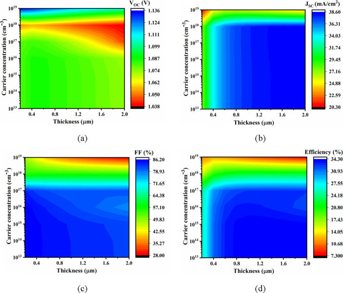
The thickness and carrier concentration of the absorber layer are crucial factors for the improvement of the thin-film PV cell’s efficiency. They affect photocarrier generation and the extraction. The rates of carrier generation and recombination increase as the absorber layer thickness increase. For analyzing the impact of the absorber layer thickness as well as carrier concentration on photovoltaic performance parameters of our designed cells, the parameters of other layers have been kept constant. The carrier concentration and thickness of the MoS2 absorber layer have been changed from 1013 to 1019 cm–3 and 200 to 2000 nm, correspondingly as illustrated in Figure 2. For the thickness range of 100 to 400 nm with increasing doping 1013 to 1016 cm–3, there is a slight increase in VOC, which then starts to decrease from 1017 to 1018 cm–3. For the thickness range of 500 to 2000 nm with increasing carrier concentration from 1013 to 1015 cm–3, there is a rise in VOC, whereas for the carrier concentration from 1016 to 1018 cm–3 there is a decline in VOC. The value of JSC increases as the MoS2 thickness rises from 200 to 2000 nm with increasing doping 1013 to 1018 cm–3 as illustrated in Figure 2b. The absorption of longer wavelength photons rises as the thickness of MoS2 grows, which results in a rise in JSC. The longer diffusion lengths of charge carriers are affected by the larger absorber layer, which enhances photogenerated carrier recombination via SRH recombination. The charge carriers may recombine before arriving at the charge accumulating metal contact if the absorber is too thick.41 The lifetime of light -induced electrons shortens as the acceptor carrier concentration raises that limiting collection of carriers at the interface as a result, JSC reduces.42 Due to high carrier concentration (>1018 cm–3) of the MoS2 absorber layer, JSC starts to decrease. The FF also reduces with the enhancement of the doping density (>1016 cm–3) with lower thickness (>1000 nm) in MoS2 absorber layer as represented in Figure 2c. The PCE decreases due to the combined reduction of the JSC and FF at higher doping density (>1016 cm–3) and absorber layer thickness (>1000 nm). The PCE is similarly shown to be approximately independent of MoS2 carrier concentration until 1016 cm–3 but rapidly drops if MoS2 carrier concentration exceeds 1016 cm–3. This occurrence might be caused due to the rise in recombination rate as well as collisions between PGCs at greater carrier concentrations as demonstrated in Figure 2d.43 Another explanation is that when the concentration rises, the JSC begins to fall due to a decrease in minority carrier diffusion length. There is also the commencement of heavy doping effects, in which the dark current increases rather than decreases as it does at lower doping levels. As a result, the dark current starts to rise.44 The optimal PCE of 33.32% has been achieved at MoS2 layer thickness and carrier concentration of 800 nm and 1016 cm–3, respectively for reducing the device fabrication cost.
Figure 2.
Concurrent impact of photovoltaic performance parameters due to variation of absorber thickness and carrier concentration (a) VOC (b) JSC (c) FF, and (d)η.
3.2. Impact of Performance Due to Variation of Thickness and Defects Density of MoS2 Absorber Layer
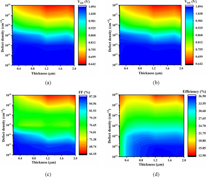
To examine the influence of defect density on the performance of the solar cell, the defect density and thickness of the MoS2 absorber layer have been changed from 1012 to 1018 cm–3 and 200 to 2000 nm, respectively, as illustrated in Figure 3. When the defect density of MoS2 is more than 1014 cm–3, the solar cell performance parameters degrade significantly. For changing the bulk defect density and absorber layer thickness from 1012 to 1018 cm–3 and 200–2000 nm, the PCE, FF, JSC, and VOC of ITO/TiO2/MoS2/In2Te3 structures drops from 36.5 to 9.5%, 87 to 64%, 38.5 to 22 mA/cm2, and 1.094 to 0.64 V respectively. When the thickness is greater than 1500 nm and the defect density is less than 1014 cm–3, the highest VOC of 1.093 V has been attained; however when the defect density is larger than 1014 cm–3, the VOC declines dramatically to 0.6342 V as represented in Figure 3a. The maximum value (38.5 mA/cm2) of JSC attained at a thickness (>1500 nm) as well as defect density (<1014 cm–3) is demonstrated in Figure 3b. When the thickness of the absorber reduces, a sharp drop in JSC may also be observed at the defect’s density larger than 1017 cm–3. The FF behaves in the same way as VOC as illustrated in Figure 3c. The highest value (>32%) of conversion efficiency has been achieved in the thickness range of 400–2000 nm and defect density (up to 1014 cm–3) as illustrated in Figure 3d.
Figure 3.
Concurrent impact of PV performance parameters due to variation of absorber thickness and defect density (a) VOC, (b) JSC, (c) FF, and (d) η.
The presence of defects in the MoS2 absorber layer increases the SRH recombination rate, which decreases the number of PGCs, which assists in decreasing the value of VOC, JSC, FF, and PCE.45 The optimized value of PCE 33.33% has been determined including VOC of 1.0893 V, JSC of 37.223 mA/cm2, and FF of 82.58% at constant thickness of 800 nm MoS2 absorber layer and defect concentration of 1014 cm–3.
3.3. Effect of Thickness and Carrier Concentration of In2Te3 BSF on Performance Parameters
By establishing a strong field near the rear electrode, the back surface field (BSF) has been utilized to maximize SC efficiency by reducing SRV. The influence of the thickness and doping concentration of the In2Te3 BSF on the device’s performance has been evaluated.
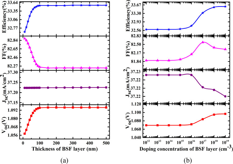
The In2Te3 BSF layer’s thickness has been changed from 10 to 500 nm at 1 × 1017 cm–3 acceptor doping concentration for analyzing the impact on device performance parameters as illustrated in Figure 4a.
Figure 4.
Impact of the PV parameter due to variation of (a) In2Te3 layer thickness and (b) doping concentration of the In2Te3 layer.
As the In2Te3 BSF layer thickness increases, device performance begins to deteriorate. The main reason for this degradation is that the enhancement of BSF thickness causes a rise in series resistance. This increase in resistance due to the BSF layer thickness affects the FF and PCE of a device.46
Figure 4b depicts the effect of doping concentration of In2Te3 on PV parameters at a thickness of 50 nm, and the influence of carrier concentration on the In2Te3 BSF layer has been studied in the range of 1012 to 1019 cm–3. All the PV parameters increase significantly with rising peak doping concentration starting from 1016 cm–3 excluding the JSC.
Higher levels of acceptor doping concentrations generate potential at the In2Te3/MoS2 junction, reducing carrier recombination loss. Due to the increased carrier concentration, the Fermi level of BSF moves toward the valence band (VB) allowing for rapid accumulation of holes at the rear electrode by developing an ohmic contact with rear-metal contact (Ni).47 The optimal thickness and acceptor concentration have been chosen 50 nm and 1017 cm–3 for the In2Te3 BSF layer for reducing the device fabrication cost.
3.4. Influence of Thickness Variation, Carrier Concentration, and Defect Density of the Buffer Layer on PV Performances
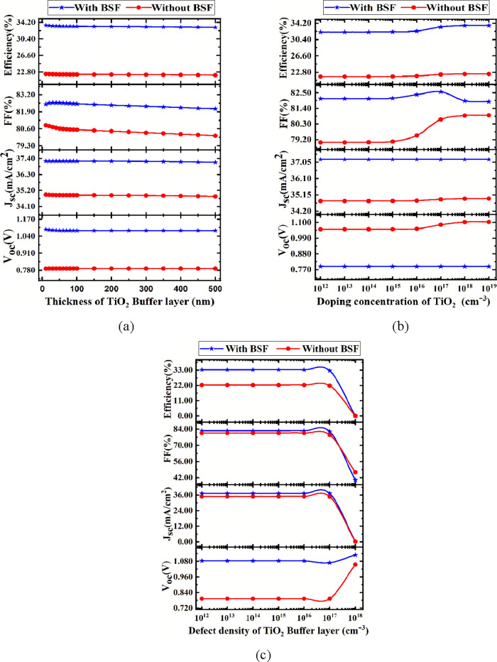
The PV parameters of the MoS2-based thin film heterojunction PV cell with and without BSF have been changed, when the buffer layer’s thickness varies. The thickness changes from 10 to 500 nm. When the TiO2 buffer layer thickness is increased, all of the PV parameters are slightly reduced for both with and without the BSF structure as illustrated in Figure 5a.
Figure 5.
Impact of the PV parameter due to variation of (a) TiO2 layer thickness (b) doping concentration in TiO2, and (c) defect density in the TiO2 buffer layer.
The influence of TiO2 buffer layer doping concentration on PV parameters has also been evaluated as depicted in Figure 5b. Our findings imply that all PV parameters enhances with increasing carrier concentration starting at 1014 cm–3 for the structure with BSF. The VOC, JSC, and PCE have been increasing from 1.0521 to 1.1042 V, 37.22331 to 37.22353 mA/cm2, and 32.25 to 33.65%, respectively, for the doping concentrations ranging from 1012 and 1019 cm–3, respectively, while VOC falls from 0.7931 to 0.7928 V and JSC, FF, and η rise from 34.79023 to 34.93195 mA/cm2, 79 to 80.92% and 21.8 to 22.41% respectively for changing doping concentrations from 1012 and 1019 cm–3 for the structure without BSF. The increase of TiO2 buffer layer thickness means photogenerated electrons need to flow long distances to reach the front contact, which increase the carrier recombination rate. Therefore, the number of carriers as well as PV performance parameters reduces, while the increase of doping density in TiO2 increases the number of carriers, which contributes to increase efficiency parameter.15 The optimum value of thickness and doping concentration has been determined to be 50 nm and 1017 cm–3, respectively for reducing device fabrication cost.
For the n-type buffer layer, we employed single-acceptor type bulk defects. The defect density of the buffer layer TiO2 has been changed from 1012 to 1018 cm–3, whereas the layer’s defect concentration remained constant at 1014 cm–3 displayed in Figure 5c. All the parameters, excluding VOC, decrease rapidly with rising bulk defect density beginning from 1017 cm–3 for both with and without the BSF structure. The presence of defect density in the TiO2 layer contributes to increase the SRH recombination rate, which degrade the overall performance of the SC.38 The defect density has been kept at 1015 cm–3 for determining optimum performance.38
3.5. Impact of Interface Defect on Performance Parameters
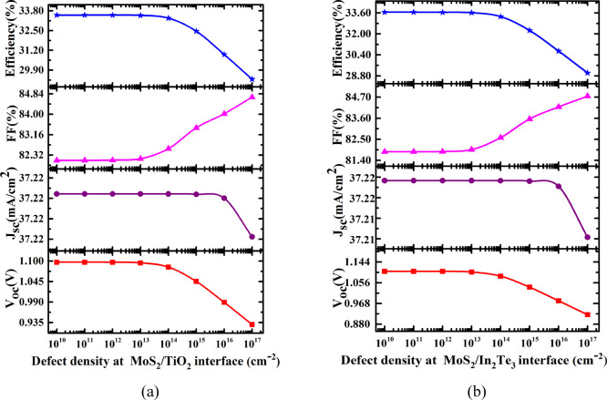
Interface defect state impacts on the output parameters significantly similar to the bulk defects. Figure 6a,b depicts the consequence of an interfacial defect at MoS2/TiO2 and In2Te3/MoS2 on the PV parameters of a newly developed MoS2-based solar cell. The interface defect concentration for both MoS2/TiO2 and In2Te3/MoS2 interfaces has been varied from 1010 to 1017 cm–2 in this numerical analysis, while the other parameters remained fixed. It has been noticed from Figure 6a,b for both interfaces that all the PV parameters degrade significantly with increasing defect density starting from 1014 cm–2. The PCE decreased from 33.65 to 29.02% and 32.52 to 29.02% for changing defect concentration from 1010 to 1017 cm–2for the In2Te3/MoS2 and MoS2/TiO2 respectively. To obtain optimal PV performance of MoS2 solar cells, defect density has been kept 1014 cm–2 for both interfaces. The trap states present at the interface act as a recombination center, which contribute to the reduction of the number of photogenerated carriers as well as inhibit the carrier collection.48 Both of these interface state-related defects contribute to a significant reduction in performance parameters.
Figure 6.
Influence of defect at (a) MoS2/TiO2 and (b) MoS2/In2Te3 interfaces on PV parameters.
3.6. Impact of Temperature on Cell Performance
The working temperature of the proposed MoS2-based photovoltaic cell must be regulated to achieve stability as demonstrated in Figure 7. The PV parameters of MoS2-based heterojunction with and without BSF are considerably reduced when the temperature increases from 275 to 475 K. The PCE of ITO/TiO2/MoS2/In2Te3 and ITO/TiO2/MoS2 structures is determined to be 34.36 and 23.79%, respectively at 275 K, but it falls to 25.45 and 11.46%, respectively due to the rise in operating temperature at 475 K.
Figure 7.
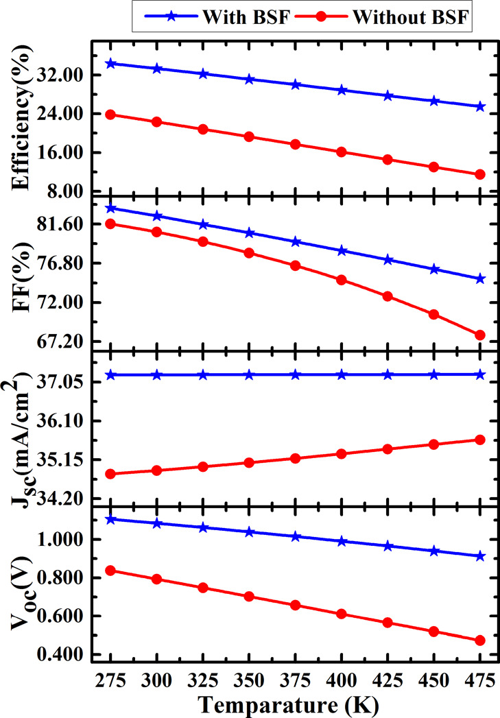
Influence of performance parameters due to variation of working temperature in MoS2-based SC with and without BSF.
These simulation results also represent that a MoS2 solar cell with BSF has better thermal consistency than a structure without BSF.37 At high temperatures, more electron–hole pairs are generated for a given irradiance that maintains a constant value of JSC. The rise in the working temperature causes to reduce band gap of MoS2 and the reverse saturation current also enhances, which results in a decrease in VOC, FF, and efficiency. In the previous publications, the consequences of PCE degradation as working temperatures were generally well acknowledged in refs (49−51).
When the temperature of PV solar cell rises, the height of the bandgap energy shrinks, resulting in a small increase of JSC. As a result, the solar cells VOC would be reduced. As a result, the reduction of VOC as well as insignificant rise of JSC leads to a fall in FF and PCE of the photovoltaic cells at higher temperature.51
3.7. Study of the Influence of SRV on the Performance Parameters
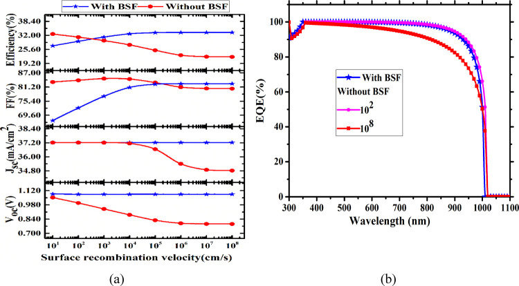
The influence of SRV at the rear contact on the performance characteristics of our proposed photovoltaic cell has been analyzed in detail as shown in Figure 8. We have alternated the SRV without and with BSF structure from 101 to 108 cm/s. All the PV parameters of ITO/TiO2/MoS2 degrade significantly with increasing SRV. The recombination of electron and holes happens at higher SRV before reaching metal contact. By inserting an addition layer called BSF, it is possible to overcome this problem. Figure 8a illustrates that the FF and PCE of ITO/TiO2/MoS2/In2Te3 structure increase with increasing SRV and at the same time VOC and JSC remain constant. The minority carrier’s lifetime as well as diffusion length has been dramatically reduced because of the rapid recombination of electrons and holes at high SRV, resulting in a decline in PV performance parameters.47 The photons with low energy absorb in the thick absorber layer despite having a high SRV; it helps to achieve a high FF and PCE because of the high absorption coefficient.52
Figure 8.
Impact of surface recombination velocity function on (a) performance parameters and (b) EQE.
The external quantum efficiency (EQE) curve is shown in Figure 8b, at three distinct SRV: 102, 108 cm/s (without In2Te3), and 107 cm/s (with In2Te3). At higher SRV, the EQE of the solar cell structure without In2Te3 reduces compared with the solar cell with In2Te3 at longer wavelength at higher SRV. As the rate of SRV rises, the electron and hole begin to recombine at the rear contact surface due to the absence of In2Te3 degrading the solar cell performance parameters.37
3.8. Effect of Capacitance–Voltage (C–V) on Solar Cell
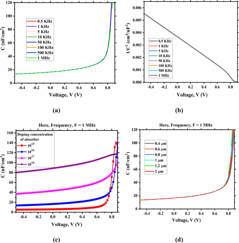
The C–V analysis has been performed in the range of frequency from 0.5 kHz to 1 MHz to investigate the consistency of the results. The depletion and diffusion capacitances are associated with the p–n junctions. The value of depletion capacitance is larger than diffusion capacitance at reverse bias voltage, whereas the diffusion capacitance dominates at the forward bias.
The capacitance of the p–n junction solar cell is found to be 16 nF cm–2 at the zero bias voltage as demonstrated in Figure 9a. The capacitance rises exponentially with the enhancement of the polarization potential at particular frequency. The insensitiveness of the absorber traps at any frequencies shows this tendency. At the reverse bias, the effective traps do not help to minimize the effective charge, which results in reduced capacitance.53
Figure 9.
Effect of C–V on solar cell (a) varying frequency, (b) 1/C2–V curve, (c) varying doping of absorber, and (d) varying thickness of absorber.
The Mott–Schottky plot of the Al/ITO/TiO2/MoS2/In2Te3/Ni PV cell has been represented in Figure 9b. The flat-band potential of the proposed SC originates from the intersection of the 1/C2 plot with the voltage axis. The negative slope of the plot indicates that holes are majority carriers as well as the space charge area largely occupies the p-type MoS2 layer. The high carrier density in the MoS2 layer may have originated from the PGCs owing to the exposure of sunlight. The marginal deviation for 1/C2 may be as a consequence of the localized deep states in the absorber layer. The impact of the deep states is not dominant and the main effect is caused by the modulation of the majority carriers.53
Figure 9c represents C–V properties of MoS2 SC due to the variation of the absorber layer doping concentration. The value of capacitances increases with the rise of the forward bias voltage and act as Mott–Schottky junctions. The lower value of the built-in potential originated from Mott–Schottky plot under the illumination of sunlight, which can be assigned to the capacitance developed from the photogenerated carrier in side lower mobility materials. The rise of doping density enhances the charge accumulation at the interface, which contributes to the rise of the value of capacitance, which is reported in a previous study.54
Figure 9d demonstrates the change of capacitance due to the change of bias voltage at different thicknesses at a constant frequency of 1 MHz. The value of capacitance change due to the variation of thickness is almost insignificant. After the voltage of 0.80 V, the value of capacitance rises dramatically with the increase of voltage. The same type tendency of the capacitance on the thickness and voltage has been published in the previous article.55
3.9. Device Output Performance
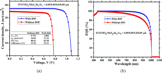
The simulated current density–voltage (J–V) and EQE curves for the optimized MoS2-based photovoltaic cell with and without BSF layer have been demonstrated in Figure 10 under the 1.5AM solar illumination. The estimated values of the VOC, JSC, FF, and PCE is 1.084 V, 37.22 mA/cm2, 82.58%, and 33.32% of the proposed Al/ITO/TiO2/MoS2/In2Te3/Ni heterostructure PV cell determined from numerical simulation.
Figure 10.
(a) J–V curve and (b) EQE curve of the cell designed with and without the BSF structure.
The output parameters of Al/ITO/TiO2/MoS2/Ni structure have been found to be 0.793 V, 34.89 mA/cm2, 80.62%, and 22.30%. The determined PV parameters from the numerical simulation of the SC with In2Te3 are much higher than those of the structure without BSF.
The J–V curve is a powerful tool to estimate the recombination loss of the carrier in the SC. The introduction of In2Te3 BSF in the proposed SC structure results in a lower value of recombination current density. In addition, it has been demonstrated that the total minority carrier recombination current density of MoS2 solar cell with In2Te3 BSF layer estimated to be smaller than that of the reference SC. The simulated results indicate that photogenerated carriers reflected back toward the MoS2/TiO2 rather than recombination at the back contact. Therefore, the inclusion of the In2Te3 BSF layer in the reference Al/ITO/TiO2/MoS2/Ni structure contributes to enhanced performance parameters by reducing carrier recombination loss.56
Furthermore, the efficiency enhancement may be justified by calculating the lattice mismatch between absorber and BSF layer (Table 4) using the following equation:15,57
where, δ, as, and ae are the lattice mismatch, substrate, and epitaxial thin film lattice constant, respectively.
Table 4. Lattice Mismatch between Absorber/BSF Values Have Been Compared with Lattice Mismatch (%) of the BSFs or HTLs Employed in the Previous Studies.
| layer | lattice parameters | lattice mismatch | ||
|---|---|---|---|---|
| a (Å) | B (Å) | C (Å) | ||
| MoS2 | 3.15 | 3.15 | 12.3 | |
| In2Te3 | 13.417 | 13.417 | 13.417 | 8.69% |
| SnS | 3.82 | 3.82 | 6.257 | 19.22% |
| Sb2S3 | 11.31 | 3.8363 | 11.22 | 19.64% |
The value of the lattice constant for the different materials has been taken from previous research.58−60 The lattice mismatch of MoS2 and In2Te3 is 8.69%, which is lower than that of the HTLs employed in the previous studies. The primary cause of non-radiative recombination is the presence of defect and interface defect density, which results in carrier losses and a drop in output voltage.61 The lower value of lattice mismatch between In2Te3 and MoS2 results in the reduction of interface defect density as well as recombination loss significantly. Thus, the insertion of the In2Te3 BSF layer in MoS2 reference enhances the performance parameters significantly. The absence of BSF in the Al/ITO/TiO2/MoS2/Ni reference structure exhibits low VOC due to the rise of minority carrier recombination. As a result, the device’s performance parameters have been affected.
Figure 10b shows the EQE of both the optimized cells. High EQE has been demonstrated for the proposed solar cell with In2Te3 compared to the without In2Te3 structure. The insertion of the In2Te3 BSF layer in the proposed SC structure decreases the PGC recombination by creating strong back surface electric fields at the In2Te3/MoS2 interface and enhances the absorption edge at the higher wavelength range, which contribute to maximize the overall performance parameters of the SC.37
Table 5 compares the evolution of MoS2-based solar cell configurations investigated by various research groups. The PCE increases from 19.62 to 21.39% according to the earlier reported experimental and numerical simulations. In comparison to the published values, the improved VOC, JSC, and PCE have been achieved by this numerical simulation. The presence of deep-level defect levels inside the MoS2 absorber’s energy band gap as well as interface-associated defects degrades the performance parameters of the previously published structures. The practical performance of MoS2 photovoltaic cells was quite poor compared to the numerically determined values. The carrier recombination at the rear and front contact and misalignment of bands at the BSF/absorber and absorber/buffer is also responsible for the reduction. The high surface carrier recombination at MoS2/back contact results in a lower value of the efficiency parameters. The P+-type In2Te3 BSF layer introduced between an absorber and a back contact layer acts as a passivation layer and enhances the efficiency parameters VOC, JSC, FF, and PCE by reducing the minority carrier recombination loss. Moreover, the formation of p+–p junction creates strong electric field along the MoS2 absorber layer due to the insertion of the In2Te3 BSF layer, which reflect the photo-generated carriers toward the front contact and enhances the overall efficiency parameters.
Table 5. Upgraded Performance Parameters Values Have Been Compared with Previously Published Reportsa.
| number | type of analysis | formation of cell | MoS2 depth (nm) | JSC (mA/cm2) | VOC (mV) | FF (%) | η (%) | ref |
|---|---|---|---|---|---|---|---|---|
| 01 | Exp. | ITO/MoS2 | 110 | 0.7 | (24) | |||
| 02 | Exp. | ITO/MoS2 | 220 | 1.8 | (24) | |||
| 03 | Exp. | ITO/TiO2/MoS2/P3HT | 4.7 | 560 | – | 1.3 | (25) | |
| 04 | Exp. | n-MoS2 (monolayer)/p-Si | 22.32 | 410 | 57.26 | 5.23 | (27) | |
| 05 | Exp. | WSe2/MoS2 | ∼10 | (26) | ||||
| 06 | Theo. | n-ZnO/n-CdS/p-MoS2 | 1000 | 19.62 | (28) | |||
| 07 | Theo. | ITO/n-ZnSe/p-MoS2 | 27.84 | 820 | 84.6 | 19.48 | (29) | |
| 08 | Theo. | ITO/n-ZnSe/p-MoS2/p+-SnS | 1000 | 29.89 | 841 | 85 | 21.39 | (29) |
| 09 | Theo. | Al/FTO/n-CdS/p-MoS2/Ni | 1000 | 34.11 | 760 | 82.80 | 21.61 | (62) |
| 10 | Theo. | Al/FTO/CdS/MoS2/p+-Sb2S3/Ni | 1000 | 35.20 | 920 | 85.51 | 27.96 | (62) |
| 11 | Theo. | ITO/TiO2/MoS2 | 800 | 34.89 | 793 | 80.62 | 22.30 | this work |
| 12 | Theo. | ITO/TiO2/MoS2/In2Te3 | 800 | 37.22 | 1084 | 82.58 | 33.32 | this work |
Exp. = experimental work and Theo. = theoretical work.
4. Conclusions
A comparative analysis of the performance parameters of MoS2-based TFSCs with and without an In2Te3 BSF layer has been done in this numerical simulation using SCAPS-1D. Instead of the utilization of conventional toxic cadmium sulfide (CdS) as a buffer layer, TiO2 with optimum thickness has been employed as a buffer layer material. The optimal thicknesses for the TiO2 buffer layer, MoS2 absorber layer, and In2Te3 BSF layer have been chosen to be of 50, 800, and 50 nm, respectively. The optimized values of carrier concentration have also been selected to be approximately to 1017, 1016, 1017 cm–3, respectively. The peak defect concentration in the p-MoS2 absorber layer and the interface defect at MoS2/TiO2 and In2Te3/MoS2 have been calculated to be 1014 eV–1 cm–3 and 1014 cm–2 and 1014 cm–2, correspondingly. The numerically simulated determined value PCE is 33.32%, including VOC of 1.084 V, JSC of 33.22 mA/cm2, and FF of 82.58% of the suggested MoS2-based heterojunction with the In2Te3, which is greater than that without In2Te3 PV cell. The present research work provides guidelines for the realization of a highly efficient MoS2-based PV cell in a cost-effective way.
Acknowledgments
The authors would like to express their sincere gratitude to Dr. Marc Burgelman and his colleagues at the EIS Department at the University of Gent in Belgium for providing us with the opportunity to conduct research using the SCAPS-1D software.
Glossary
List of Abbreviations
- MoS2
molybdenum disulfide
- In2Te3
indium telluride
- TiO2
titanium dioxide
- ITO
indium tin oxide
- BSF
back surface field
- VOC
open circuit voltage
- JSC
short circuit current
- FF
fill factor
- PCE
power conversion efficiency
- C–V
capacitance–voltage
- SRV
surface recombination velocity
- TMDs
transition metal dichalcogenides
- CBM
conduction band minimum
- CBO
conduction band offset
- TW
terawatts
- TFSCs
thin-film solar cells
- SC
solar cell
- PV
photovoltaic
- CdTe
cadmium telluride
- CIGS
copper indium gallium selenide
- CZTS
copper zinc tin sulfide
- HTL
hole transport layer
- PGC
photogenerated carrier
- PGHs
photogenerated holes
- PGEs
photogenerated electrons
- EQE
external quantum efficiency
- CdS
cadmium sulfide
- SRH
Shockley–Read–Hall
The authors declare no competing financial interest.
References
- Meissner D.Solar Power Implications of Our Climate Crisis, 2020; pp 2–3.
- Matin Bhuiyan M. A.Development of High Efficiency Ultra-Thin CdTe Solar Cell with Back Surface Field. Ph.D. Thesis, Univ. Kebangs, Malaysia, 2011.
- Andreani L. C.; Bozzola A.; Kowalczewski P.; Liscidini M.; Redorici L. Silicon Solar Cells: Toward the Efficiency Limits. Adv. Phys.: X 2019, 4, 1548305 10.1080/23746149.2018.1548305. [DOI] [Google Scholar]
- Lee T. D.; Ebong A. U. A Review of Thin Film Solar Cell Technologies and Challenges. Renewable Sustainable Energy Rev. 2017, 70, 1286–1297. 10.1016/j.rser.2016.12.028. [DOI] [Google Scholar]
- Alzahrani G. S.; Alzahrani F. S.; Nahhas A. M. Study of the Specific Factors Effecting the PV Solar Cell’s Efficiency in Saudi Arabia. Sustain. Energy 2020, 8, 6–11. 10.12691/rse-8-1-2. [DOI] [Google Scholar]
- Imamzai M.; Aghaei M.; Thayoob Y. H. A Review on Comparison between Traditional Silicon Solar Cells and Thin-Film CdTe Solar Cell. Proc. Natl. Grad. Conf. 2011, 2012, 8–10. [Google Scholar]
- Green M. A.; Hishikawa Y.; Dunlop E. D.; Levi D. H.; Hohl-Ebinger J.; Ho-Baillie A. W. Y. Solar Cell Efficiency Tables (Version 52). Progr. Photovolt.: Res. Appl. 2018, 26, 427–436. 10.1002/pip.3040. [DOI] [Google Scholar]
- Lee C. T.; Lu K. F.; Tseng C. Y. Carrier Drift Velocity Balance Mechanism in Si-Based Thin Film Solar Cells Using Graded Microcrystalline SiGe Absorption Layer. Sol. Energy 2015, 114, 1–7. 10.1016/j.solener.2015.01.023. [DOI] [Google Scholar]
- Paudel N. R.; Wieland K. A.; Compaan A. D. Ultrathin CdS/CdTe Solar Cells by Sputtering. Sol. Energy Mater. Sol. Cells 2012, 105, 109–112. 10.1016/j.solmat.2012.05.035. [DOI] [Google Scholar]
- Mostefaoui M.; Mazari H.; Khelifi S.; Bouraiou A.; Dabou R. Simulation of High Efficiency CIGS Solar Cells with SCAPS-1D Software. Energy Procedia 2015, 74, 736–744. 10.1016/j.egypro.2015.07.809. [DOI] [Google Scholar]
- Yang J.; Banerjee A.; Guha S. Conversion Efficiencies Triple-Junction Amorphous Silicon Alloy Solar Cell with 14.6% Initial and 13.0% Stable Conversion Efficiencies. Appl. Phys. Lett. 1997, 70, 2975–2977. 10.1063/1.118761. [DOI] [Google Scholar]
- Gloeckler M.; Sankin I.; Zhao Z. CdTe Solar Cells at the Threshold to 20% Efficiency. Int. J. Phitovolt. 2013, 3, 1389–1393. 10.1109/JPHOTOV.2013.2278661. [DOI] [Google Scholar]
- Lee T. D.; Ebong A. U. A Review of Thin Fi Lm Solar Cell Technologies and Challenges. Renewable Sustainable Energy Rev. 2017, 70, 1286–1297. 10.1016/j.rser.2016.12.028. [DOI] [Google Scholar]
- Katagiri H.; Jimbo K.; Maw W. S.; Oishi K.; Yamazaki M.; Araki H.; Takeuchi A. Development of CZTS-Based Thin Fi Lm Solar Cells. Thin Solid Films 2009, 517, 2455–2460. 10.1016/j.tsf.2008.11.002. [DOI] [Google Scholar]
- Atowar Rahman M. Enhancing the Photovoltaic Performance of Cd-Free Cu2ZnSnS4 Heterojunction Solar Cells Using SnS HTL and TiO2 ETL. Sol. Energy 2021, 215, 64–76. 10.1016/j.solener.2020.12.020. [DOI] [Google Scholar]
- Choi W.; Choudhary N.; Han G. H.; Park J.; Akinwande D.; Lee Y. H. Recent Development of Two-Dimensional Transition Metal Dichalcogenides and Their Applications. Mater. Today 2017, 20, 116–130. 10.1016/j.mattod.2016.10.002. [DOI] [Google Scholar]
- Li X.; Zhu H. Two-Dimensional MoS2: Properties, Preparation, and Applications. J. Mater. 2015, 1, 33–44. 10.1016/j.jmat.2015.03.003. [DOI] [Google Scholar]
- Manzeli S.; Ovchinnikov D.; Pasquier D.; Yazyev O. V.; Kis A. 2D Transition Metal Dichalcogenides. Nat. Rev. Mater. 2017, 2, 17033. 10.1038/natrevmats.2017.33. [DOI] [Google Scholar]
- Zaidi B.; Shekhar C.; Hadjoudja B.; Gagui S.; Chouial B. Optimization of Highly Efficient Monolayer MoSe2 Based Solar Cells. Acta Phys. Pol. A 2019, 136, 495–497. 10.12693/APhysPolA.136.495. [DOI] [Google Scholar]
- Chhowalla M.; Shin H. S.; Eda G.; Li L. J.; Loh K. P.; Zhang H. The Chemistry of Two-Dimensional Layered Transition Metal Dichalcogenide Nanosheets. Nat. Chem. 2013, 5, 263–275. 10.1038/nchem.1589. [DOI] [PubMed] [Google Scholar]
- Wang X.; Huang L.; Peng Y.; Huo N.; Wu K.; Xia C.; Wei Z.; Tongay S.; Li J. Enhanced Rectification, Transport Property and Photocurrent Generation of Multilayer ReSe2/MoS2 p–n Heterojunctions. Nano Res. 2016, 9, 507–516. 10.1007/s12274-015-0932-6. [DOI] [Google Scholar]
- Yang K.; Liu T.; Zhang X. D. Bandgap Engineering and Near-Infrared-II Optical Properties of Monolayer MoS2: A First-Principle Study. Front. Chem. 2021, 9, 1–13. 10.3389/fchem.2021.700250. [DOI] [PMC free article] [PubMed] [Google Scholar]
- Kwak J. Y. Absorption Coefficient Estimation of Thin MoS 2 Film Using Attenuation of Silicon Substrate Raman Signal. Results Phys. 2019, 13, 102202 10.1016/j.rinp.2019.102202. [DOI] [Google Scholar]
- Paquin F.; Rivnay J.; Salleo A.; Stingelin N.; Silva C. Multi-Phase Semicrystalline Microstructures Drive Exciton Dissociation in Neat Plastic Semiconductors. J. Mater. Chem. C 2015, 3, 10715–10722. 10.1039/b000000x. [DOI] [Google Scholar]
- Shanmugam M.; Bansal T.; Durcan C. A.; Yu B. Molybdenum Disulphide/Titanium Dioxide Nanocomposite-Poly 3-Hexylthiophene Bulk Heterojunction Solar Cell. Appl. Phys. Lett. 2012, 100, 1–5. 10.1063/1.3703602. [DOI] [Google Scholar]
- Cho A. J.; Song M. K.; Kang D. W.; Kwon J. Y. Two-Dimensional WSe2/MoS2 p-n Heterojunction-Based Transparent Photovoltaic Cell and Its Performance Enhancement by Fluoropolymer Passivation. ACS Appl. Mater. Interfaces 2018, 10, 35972–35977. 10.1021/acsami.8b12250. [DOI] [PubMed] [Google Scholar]
- Tsai M. L.; Su S. H.; Chang J. K.; Tsai D. S.; Chen C. H.; Wu C. I.; Li L. J.; Chen L. J.; He J. H. Monolayer MoS2 Heterojunction Solar Cells. ACS Nano 2014, 8, 8317–8322. 10.1021/nn502776h. [DOI] [PubMed] [Google Scholar]
- Rashid H.; Rahman K. S.; Hossain M. I.; Tabet N.; Alharbi F. H.; Amin N. Prospects of Molybdenum Disulfide (MoS2) as an Alternative Absorber Layer Material in Thin Film Solar Cells from Numerical Modeling. Chalcogenide Lett. 2014, 11, 397–403. [Google Scholar]
- Dey M.; Shahriar M. F.; Ali A.; Dey M.; Das N. K.. Design and Optimization of an Efficient Molybdenum Disulfide (MoS2) Solar Cell with Tin Sulfide BSF. 2nd Int. Conf. Electr. Comput. Commun. Eng. ECCE 2019, 2019; pp 1–5.
- Choi Y. C.; Seok S. I. Efficient Sb2S3-Sensitized Solar Cells via Single-Step Deposition of Sb2S3 Using S/Sb-Ratio-Controlled SbCl3-Thiourea Complex Solution. Adv. Funct. Mater. 2015, 25, 2892–2898. 10.1002/adfm.201500296. [DOI] [Google Scholar]
- Versavel M. Y.; Haber J. A. Structural and Optical Properties of Amorphous and Crystalline Antimony Sulfide Thin-Films. Thin Solid Films 2007, 515, 7171–7176. 10.1016/j.tsf.2007.03.043. [DOI] [Google Scholar]
- Eisele W.; Ennaoui A.; Schubert-Bischoff P.; Giersig M.; Pettenkofer C.; Krauser J.; Lux-Steiner M.; Zweigart S.; Karg F. XPS, TEM and NRA Investigations of Zn(Se,OH)/Zn(OH)2 Films on Cu(In,Ga)(S,Se)2 Substrates for Highly Efficient Solar Cells. Sol. Energy Mater. Sol. Cells 2003, 75, 17–26. 10.1016/S0927-0248(02)00104-6. [DOI] [Google Scholar]
- Cao Y.; Zhu X.; Chen H.; Zhang X.; Zhou J.; Hu Z.; Pang J. Towards High Efficiency Inverted Sb2Se3 Thin Film Solar Cells. Sol. Energy Mater. Sol. Cells 2019, 200, 109945 10.1016/j.solmat.2019.109945. [DOI] [Google Scholar]
- Bayad H.; El Manouni A.; Marí B.; Khattak Y. H.; Ullah S.; Baig F. Influence of P+-ZnTe Back Surface Contact on Photovoltaic Performance of ZnTe Based Solar Cells. Opt. Quantum Electron. 2018, 50, 259. 10.1007/s11082-018-1530-0. [DOI] [Google Scholar]
- Burgelman M.; Nollet P.; Degrave S. Modelling Polycrystalline Semiconductor Solar Cells. Thin Solid Films 2000, 361-362, 527–532. 10.1016/S0040-6090(99)00825-1. [DOI] [Google Scholar]
- Minemoto T.; Hashimoto Y.; Satoh T.; Negami T.; Takakura H.; Hamakawa Y. Cu(In,Ga)Se2 Solar Cells with Controlled Conduction Band Offset of Window/Cu(In,Ga)Se2 Layers. J. Appl. Phys. 2001, 89, 8327–8330. 10.1063/1.1366655. [DOI] [Google Scholar]
- Haque M. D.; Ali M. H.; Islam A. Z. M. T. Efficiency Enhancement of WSe2 Heterojunction Solar Cell with CuSCN as a Hole Transport Layer: A Numerical Simulation Approach. Sol. Energy 2021, 230, 528–537. 10.1016/j.solener.2021.10.054. [DOI] [Google Scholar]
- Kohnehpoushi S.; Nazari P.; Nejand B. A.; Eskandari M. MoS 2 : A Two-Dimensional Hole-Transporting Material for High-Ef Fi Ciency , Low-Cost Perovskite Solar Cells. Nanotechnology 2018, 29, 205201. 10.1088/1361-6528/aab1d4. [DOI] [PubMed] [Google Scholar]
- Mouloua D.; Kotbi A.; Deokar G.; Kaja K.; El Marssi M.; El Khakani M. A.; Jouiad M. Recent Progress in the Synthesis of MoS2 Thin Films for Sensing, Photovoltaic and Plasmonic Applications: A Review. Materials 2021, 14, 3283. 10.3390/ma14123283. [DOI] [PMC free article] [PubMed] [Google Scholar]
- Dey M.; Dey M.; Matin M. A.; Amin N.. High Performance and Stable Molybdenum Telluride PV Cells with Indium Telluride BSF. ICDRET 2016 - 4th Int. Conf. Dev. Renew. Energy Technol., 2016; pp 4–7.
- Subedi K. K.; Phillips A. B.; Shrestha N.; Alfadhili F. K.; Osella A.; Subedi I.; Awni R. A.; Bastola E.; Song Z.; Li D. B.; Collins R. W.; Yan Y.; Podraza N. J.; Heben M. J.; Ellingson R. J. Enabling Bifacial Thin Film Devices by Developing a Back Surface Field Using CuxAlOy. Nano Energy 2021, 83, 105827 10.1016/j.nanoen.2021.105827. [DOI] [Google Scholar]
- Rahman M. A. Design and Simulation of a High-Performance Cd-Free Cu2SnSe3 Solar Cells with SnS Electron-Blocking Hole Transport Layer and TiO2 Electron Transport Layer by SCAPS-1D. SN. Appl. Sci. 2021, 3, 1. 10.1007/s42452-021-04267-3. [DOI] [Google Scholar]
- Ahmmed S.; Aktar A.; Tabassum S.; Rahman M. H.; Rahman M. F.; Abu A. B. CuO Based Solar Cell with V2O5 BSF Layer: Theoretical Validation of Experimental Data. Superlattices Microstruct. 2021, 151, 106830 10.1016/j.spmi.2021.106830. [DOI] [Google Scholar]
- Zekry A.; Shaker A.; Salem M.. Solar Cells and Arrays: Principles, Analysis, and Design, 2018; vol 1.
- Taheri S.; Ahmadkhan Kordbacheh A.; Minbashi M.; Hajjiah A. Effect of Defects on High Efficient Perovskite Solar Cells. Opt. Mater. 2021, 111, 110601 10.1016/j.optmat.2020.110601. [DOI] [Google Scholar]
- Khattak Y. H.; Baig F.; Toura H.; Beg S.; Soucase B. M. Efficiency Enhancement of Cu2BaSnS4 Experimental Thin-Film Solar Cell by Device Modeling. J. Mater. Sci. 2019, 54, 14787–14796. 10.1007/s10853-019-03942-6. [DOI] [Google Scholar]
- Khatun M. M.; Sunny A.; Ahmed S. R. A. Numerical Investigation on Performance Improvement of WS2 Thin-Film Solar Cell with Copper Iodide as Hole Transport Layer. Sol. Energy 2021, 224, 956–965. 10.1016/j.solener.2021.06.062. [DOI] [Google Scholar]
- Basyoni M. S. S.; Salah M. M.; Mousa M.; Shaker A.; Zekry A.; Abouelatta M.; Alshammari M. T.; Al-Dhlan K. A.; Gontrand C. On the Investigation of Interface Defects of Solar Cells: Lead-Based vs Lead-Free Perovskite. IEEE Access 2021, 9, 130221–130232. 10.1109/ACCESS.2021.3114383. [DOI] [Google Scholar]
- Bouich A.; Hartiti B.; Ullah S.; Ullah H.; Touhami M. E.; Santos D. M. F.; Mari B. Experimental, Theoretical, and Numerical Simulation of the Performance of CuIn x Ga (1-x) S 2 -Based Solar Cells. Optik 2019, 183, 137–147. 10.1016/j.ijleo.2019.02.067. [DOI] [Google Scholar]
- Biplab S. R. I.; Ali M. H.; Moon M. M. A.; Pervez M. F.; Rahman M. F.; Hossain J. Performance Enhancement of CIGS-Based Solar Cells by Incorporating an Ultrathin BaSi2 BSF Layer. J. Comput. Electron. 2020, 19, 342–352. 10.1007/s10825-019-01433-0. [DOI] [Google Scholar]
- Abdalmageed H. I.; Fedawy M.; Aly M. H. Effect of Absorber Layer Bandgap of CIGS-Based Solar Cell with (CdS/ZnS) Buffer Layer. J. Phys.: Conf. Ser. 2021, 2128, 012009 10.1088/1742-6596/2128/1/012009. [DOI] [Google Scholar]
- Gray J. L.Handbook of Photovoltaic Science and Engineering; John Wiley & Sons: New York, 2011. [Google Scholar]
- Gupta G. K.; Garg A.; Dixit A. Electrical and Impedance Spectroscopy Analysis of Sol-Gel Derived Spin Coated Cu2ZnSnS4 Solar Cell. J. Appl. Phys. 2018, 123, 013101 10.1063/1.5002619. [DOI] [Google Scholar]
- Islam M. S.; Sobayel K.; Al-Kahtani A.; Islam M. A.; Muhammad G.; Amin N.; Shahiduzzaman M.; Akhtaruzzaman M. Defect Study and Modelling of SnX3-Based Perovskite Solar Cells with SCAPS-1D. Nanomaterials 2021, 11, 1218. 10.3390/nano11051218. [DOI] [PMC free article] [PubMed] [Google Scholar]
- Zahoo R. K.; Saleh A. N. Effect Of Carrier Concentration And Thickness Of Absorber Layer On Performance CBTS Solar Cell. Turkish J. Comput. Math. Educ. 2021, 12, 5056–5064. 10.17762/turcomat.v12i10.5281. [DOI] [Google Scholar]
- Barman B.; Kalita P. K. Influence of Back Surface Field Layer on Enhancing the Efficiency of CIGS Solar Cell. Sol. Energy 2021, 216, 329–337. 10.1016/j.solener.2021.01.032. [DOI] [Google Scholar]
- Cang Q.; Guo H.; Jia X.; Ning H.; Ma C.; Zhang J.; Yuan N.; Ding J. Enhancement in the Efficiency of Sb2Se3 Solar Cells by Adding Low Lattice Mismatch CuSbSe2 Hole Transport Layer. Sol. Energy 2020, 199, 19–25. 10.1016/j.solener.2020.02.008. [DOI] [Google Scholar]
- Ariswan; Sutrisno H.; Prasetyawati R. Crystal Structure, Optical, and Electrical Properties of SnSe and SnS Semiconductor Thin Films Prepared by Vacuum Evaporation Techniques for Solar Cell Applications. IOP Conf. Ser. Mater. Sci. Eng. 2017, 202, 012042 10.1088/1757-899X/202/1/012042. [DOI] [Google Scholar]
- Molina-Sánchez A.; Wirtz L. Phonons in Single-Layer and Few-Layer MoS2 and WS2. Phys. Rev. B: Condens. Matter Mater. Phys. 2011, 84, 155413 10.1103/PhysRevB.84.155413. [DOI] [Google Scholar]
- Kondrotas R.; Chen C.; Tang J. Sb2S3 Solar Cells. Joule 2018, 2, 857–878. 10.1016/j.joule.2018.04.003. [DOI] [Google Scholar]
- Wang K.; Gunawan O.; Todorov T.; Shin B.; Chey S. J.; Bojarczuk N. A.; Mitzi D.; Guha S. Thermally Evaporated Cu2 ZnSnS4 Solar Cells. Appl. Phys. Lett. 2010, 97, 8–11. 10.1063/1.3499284. [DOI] [Google Scholar]
- Haque D.; Ali H.; Rahman F.; Zafor A.; Islam T. Numerical Analysis for the Efficiency Enhancement of MoS 2 Solar Cell: A Simulation Approach by SCAP-1D. Opt. Mater. 2022, 131, 112678 10.1016/j.optmat.2022.112678. [DOI] [Google Scholar]


