

Abstract
The plasmonic response of a nano C-aperture is analyzed using the Vector Field Topology (VFT) visualization technique. The electrical currents that are induced on the metal surfaces when the C-aperture is excited by light is calculated for various wavelengths. The topology of this two-dimensional current density vector is analyzed using VFT. The plasmonic resonance condition is found to coincide with a distinct shift in the topology which leads to increased current circulation. A physical explanation of the phenomenon is discussed. Numerical results are presented to justify the claims. The analyses suggest that VFT can be a powerful tool for studying the physical mechanics of nano-photonic structures.
Metallic nanostructures can exhibit resonance behavior when excited by waves at optical frequencies. At these plasmonic resonance conditions, the electrical field intensity near the nanostructures can reach values that are several orders of magnitude higher than the incident field intensity. The high intensity is localized in a sub-wavelength sized region, resulting in a focal spot that is smaller than what can be achieved using diffraction limited optical elements.1–3 Such properties have led to the use of plasmonic structures for a plethora of applications ranging from optical trapping to fluorescence microscopy.1,2,4–10
The plasmonic resonance of a nanostructure depends on its geometry, dielectric functions of the materials, and the wavelength and polarization of the excitation light. When these quantities are defined, it is possible to simulate the resonance behavior by solving the Maxwell's equations. This almost exclusively requires the use of numerical solvers as most practical structures are too complex to tackle analytically. Unlike analytical approaches,11–13 numerical solution does not necessarily provide a direct insight of the underlying physics. For example, numerical results can show the field distributions during resonance but do not explain the physical mechanism triggering the resonance. As such, additional analysis tools are often employed to extract insight from the raw numerical data. For example, intuitive equivalent circuit models14,15 have been proposed. These highly useful models can be used to predict the response of the structure. The equivalent circuits are usually analogous models and do not primarily focus on the physical aspects regarding resonance. In this work, we use the topology of the induced surface current (i.e., electrical currents that are created when an incident light hits a metal surface5,6,16) to explain the resonance condition. The discussion is limited to plasmonic C-apertures which have been used in many applications.10 The field analysis and visualization tool Vector Field Topology (VFT)17–20 is used to study the induced currents. Specifically, it is shown that the resonance condition coincides with a change in the vector field topology of the induced surface current density. This distinct shift in the topology prompts an increased circulation of current around the C-aperture which leads to the stronger field enhancement. The consequence of the increased current circulation is perceived as the resonance.
Conventional vector field visualization approaches, such as contour plots, field-line, and streamlines, are general purpose in nature and do not attempt to extract scientifically significant structural features from the dataset.21 VFT is an approach of visualizing a vector field in terms of its most salient features. The approach focuses on critical/singular points (i.e., where the field value is zero) and the field/tangent lines that connect these points. The connecting lines, referred to as separatrices, segment the vector field into regions of coherent behavior.22 By focusing only on the critical points and the separatrices and eliminating other information from the visualization, the key features of the field are isolated. This gives an abstract skeletal representation of the vector field allowing one to note features that would otherwise not be discernible. In other words, VFT raises the level of abstraction above that of direct visualization, bringing to surface the key characteristics of the field. Due to its inherent analytical potential, VFT has widely been used for analyzing fluid flows.17–19,23,24 However, the use of this powerful tool in photonics research has been very limited. Besides a few excellent works on analyzing Poynting power flow,25,26 VFT has not been applied in photonics related problems. Just like it has been influential in the fluid dynamics community, VFT has the potential to be very useful in fields of optics and electrodynamics in general. The current density term in the Maxwell's equations can be an ideal analog of the flow velocity term of the Navier–Stokes equation. Thus, fluid flow analogy can be applied to electrodynamics. Since VFT can be used for any vector fields, a wide range of fields can be analyzed. Here, we demonstrate the efficacy of VFT visualization in photonics by using it to study the resonance of a nano C-aperture.
Nano C-apertures are formed by patterning thin films of noble metals (usually gold or silver) deposited on a transparent substrate (e.g., glass). Optical excitation is usually provided through the transparent substrate. The geometry of the structure along the coordinate system used throughout this paper is shown in Fig. 1. The parameter α defines the xy plane geometry. In addition of having the capabilities to focus light well beyond the diffraction limit, C-shaped nanostructures are also sensitive to the polarization of incident light.27 Due to such attractive optical properties, they have widely been used in many applications.10,28,29 As such, we have selected them as the test structure for the VFT analysis. For the current analysis, is selected. The gold film thickness is taken to be . A separate case for is discussed in the supplementary material. We posit that the analysis presented in this paper can be extended to other geometries as well. A brief discussion on VFT of other plasmonic structures is included in the supplementary material.
FIG. 1.

Plasmonic nano C-aperture. (a) 3D schematic representation, (b) xy plane geometry, and (c) xz plane geometry. The illustrations are not drawn to scale. and is assumed throughout this paper.
We start with the formal mathematical definitions associated with VFT. Let be a 2D vector field in the xy Cartesian plane. The critical points, , of are points where . However, unlike fluid velocity fields, plasmonic fields decay exponentially. Thus, the field values naturally approaches zero when observing moderately far from the source. These are, however, trivial zeros and not of significant interest. It is the non-trivial zeros of the field that should be designated as critical points. Distinguishing the critical points from the trivial zeros requires a more robust definition. In addition to having zero field values, the extra constraint of being a field minima is introduced in the definition. Hence, the set of critical points associated with the field is formally defined as
| (1) |
With the critical points defined, the integral curves, also known as tangent curves or field-lines, going through these points need to be calculated. The integral curves are smooth parametric curves with Cartesian coordinates , that are tangent to the vector field at every point:20
| (2) |
Here, t is the parameter defining the curve, is an open interval, and is the derivative of . We strictly focus on the integral curves that start at (or go through) the critical points, i.e., . These curves are known as separatrices, and can be traced by following the field direction starting from the critical points. As Eq. (2) suggests, this can be achieved by integrating along the field direction.21 This can be easily done numerically using the Euler's method.30 However, since the field is zero at the critical point, the initial direction is unknown. This issue is solved by taking the eigenvectors of the Jacobian matrix at the critical points as the initial direction. The Jacobian matrix of at p is given by
| (3) |
From Eq. (3), the eigenvalues and the corresponding eigenvectors can be calculated. Using that, the integral curves originating from the critical points (i.e., separatrices) can be determined. The set of all integral curves between the same critical points (or infinity) are bounded by separatrices. They partition the domain into regions of similar behavior and can be used to infer details about the vector field.
In addition to the eigenvectors, the eigenvalues of the Jacobian matrix at the critical points are also of interest. The critical points can be classified based on the real and imaginary parts of the eigenvalues. The real part indicates an attracting (negative) or a repelling (positive) nature while the imaginary part denotes circulation.21 Based on the possible combinations, six types of critical points (attracting node, repelling node, attracting focus, repelling focus, center, and saddle point) can be defined as shown in Fig. 2. The attracting type critical points indicate sinks, whereas the repelling types represent source regions. The types of the critical points along with the shape of the connecting separatrices can help determine the nature of the vector field.18
FIG. 2.

Classification of critical points. Ri and Ii (i = 1, 2) represent the real and imaginary components of the eigenvalues of the Jacobian matrix evaluated at the critical point, respectively.
With the mathematics of VFT defined, it can now be applied to the problem at hand. First, the electromagnetic field distribution near the nano C-aperture needs to be calculated. This is done using a standard full-field finite element solver which has been well discussed in the literature.31 For the simulation, the refractive index of gold as a function of wavelength is taken from the literature.32 The refractive index of the glass substrate is taken to be . From the electric and magnetic fields (E and H), the induced current density, , can be calculated from the Maxwell's equations.5,6,16 This quantity is taken as the 2D vector field on which the subsequent VFT analysis is performed. For a C-aperture on gold film with characteristic geometric parameter , the resonance wavelength is expected to be ∼1020 nm.33,34 A wavelength sweep ranging from 930 to 1100 nm is performed to capture various stages of the plasmonic response. For each of the representative cases, VFT analysis is performed. Details about the field calculations and the numerical implementation of the VFT are included in the supplementary material. The developed computer codes are available on GitHub.35 Results for five different wavelengths are shown in Fig. 3. In addition to the VFT, a few additional streamlines (light gray lines) are also included in the visualization. It can be seen from the VFT analysis that for wavelengths below and above the resonance, there exists a saddle point and four separatrices. For wavelengths near resonance, the saddle point vanishes and the separatrices coincide with the horizontal line. Thus, a clear shift in the topology is observed.
FIG. 3.
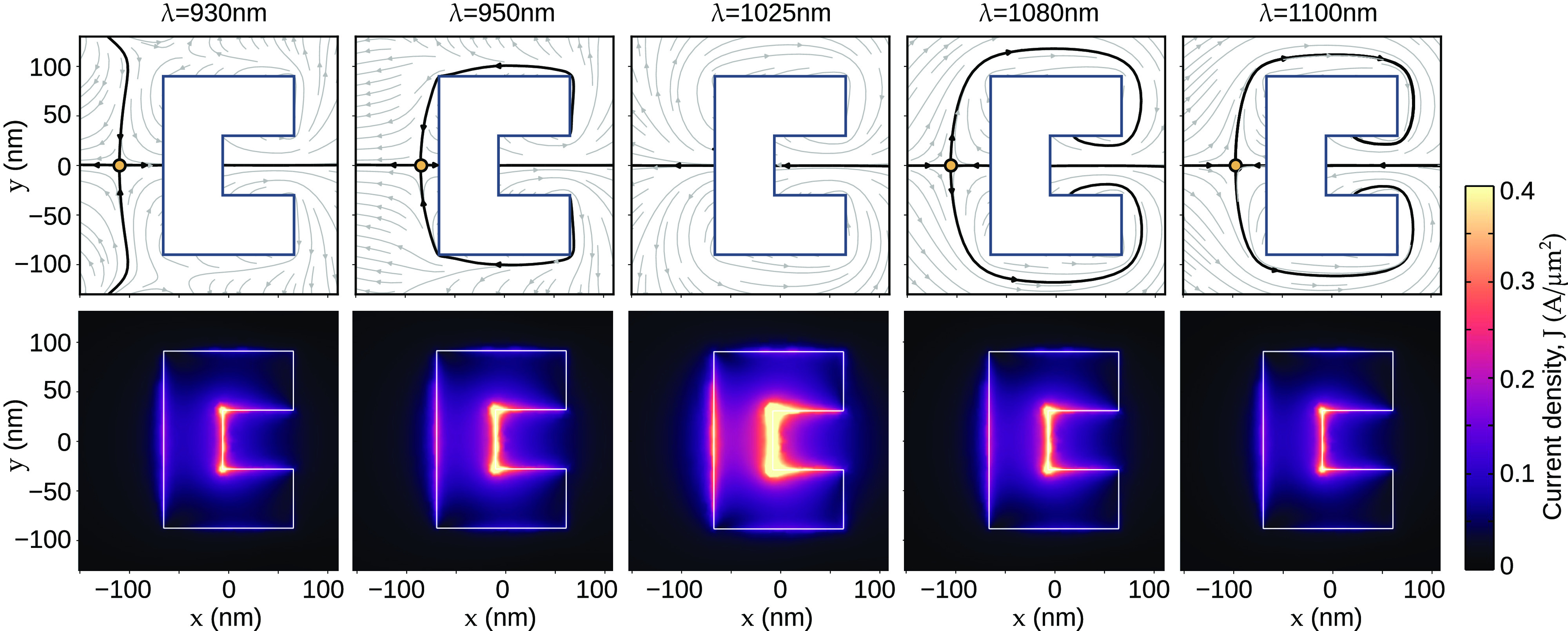
Current density on the bottom metal surface ( ) at various excitation wavelengths. The top row shows the VFT representation. Dark lines are separatrices and yellow circles are saddle points. The light gray lines are additional streamlines shown on top of the VFT. The bottom row shows the corresponding current density magnitude. The plots at the top row and the bottom row share the same x axis. Input light polarized along the x axis with an intensity of is assumed.
The implications of the topological change can be understood by noting what the saddle point and the corresponding separatrices signify. Regions bounded by the separatrices are isolated from the rest of the domain. Current flow from outside cannot cross the separatrices. Thus, the magnitude of current density (or charge accumulation) around the C-aperture edges depend on the domain enclosed by the corresponding separatrices. The horizontal separatrices along the symmetry line indicates that currents on the top half are isolated from the bottom half currents and vice versa. These line remains constant for all cases. For , the vertical separatrices curve away from the C-aperture. This indicates that no significant current circulation around the aperture edges is present. For , the separatrices curl around the edges of the aperture. Thus, the currents are circulating around the aperture. However, the regions encompassed by the separatrices and the edges of the aperture are rather small. So, a significant amount of current density fails to accumulate around the structure. Similar arguments can be made for the and 1100 nm cases. However, for case, the saddle point creating the bounding separatrices is absent. Thus, current from the entire top half of the domain is free to circulate around the top edges resulting in a large amount of current density accumulation. The exact same thing happens for the bottom half. This increased current circulation (seen from the streamlines) pushes charges near the edges of the C-aperture which results in a high electric field intensity. The current density magnitude plots shown in the bottom row of Fig. 3 are consistent with the interpretations of the VFT analysis for all five wavelength cases. As the separatrices do not enclose the waist (i.e., right middle edge) of the C-aperture, the current density is larger there compared to other edges even for non-resonant wavelengths as can be seen in the bottom row of Fig. 3. The effect of the geometry of the aperture on the current distribution and the corresponding VFT visualization can be noted from this figure as well. The separatrices bend around the arms of the C-aperture for some non-resonant cases. For C-apertures with different configurations (i.e., different height-to-width ratios),33 a similar trend is expected.
The topological shift of the current density and the resonance condition can be related more clearly by tracking the coordinates of the saddle point at various excitation wavelengths. Since the saddle point is always located along the y = 0 line (due to symmetry), only the x coordinate of the saddle point, xs, is of interest. A larger range of wavelengths is investigated for this analysis. The electric field intensity near the center of the C-aperture at the point for each wavelength is also recorded. This point is selected as it is close to the field maximum. The field intensity spectrum can be used to identify the resonance condition. The intensity spectrum and the saddle point positions at different wavelengths are shown in Fig. 4. The same x axis is used for Figs. 4(a) and 4(b) so that a one-to-one correspondence can be made between the curves. It can be clearly observed that the saddle point does not exist for wavelengths near the resonance (shaded region in Fig. 4). This is consistent with the VFT visualization shown in Fig. 3. As the resonance wavelength is determined by the geometrical parameter α34 and the material parameters, the boundary wavelengths defining the absence of the saddle point are also determined by the same parameters. Additional details about the current density near the saddle point is included in the supplementary material.
FIG. 4.

Spectral analysis of the C-aperture. (a) Normalized intensity as a function of wavelength at the point . is the magnitude of the x polarized incident electric field corresponding to the intensity . (b) Position of the saddle point in the VFT visualization of the current density as a function of incident light wavelength. The shaded region highlights wavelengths near the resonance at which the VFT contains no saddle points.
In summary, a relationship between the plasmonic resonance of a C-aperture and the topology of the induced current on the metal surface has been established. In non-resonant conditions, the induced current vector is characterized by a saddle point which reduces current circulation and charge accumulation, leading to lower electric field intensities. Near resonance, the saddle point ceases to exist resulting in increased current circulation giving rise to higher field intensities. VFT was instrumental in uncovering this mechanics which is a new way of looking at plasmonic resonance in nano C-apertures. Similar insights may be attained by applying VFT in other photonic and electrodynamic analyses as well.
See the supplementary material for details about the field simulations and the numerical implementation of the vector field topology.
Acknowledgments
This work was partially supported by the National Institutes of Health (NIH) (Grant No. R01GM138716).
AUTHOR DECLARATIONS
Conflict of Interest
The authors have no conflicts to disclose.
Author Contributions
Mohammad Asif Zaman: Conceptualization (equal); Formal analysis (equal); Investigation (equal); Methodology (equal); Visualization (equal); Writing – original draft (equal). Wei Ren: Formal analysis (equal); Validation (equal). Mo Wu: Investigation (equal); Writing – review & editing (equal). Punnag Padhy: Conceptualization (equal); Validation (equal). Lambertus Hesselink: Conceptualization (equal); Formal analysis (equal); Supervision (equal); Writing – review & editing (equal).
DATA AVAILABILITY
The data that support the findings of this study are available from the corresponding author upon reasonable request. The vector field topology code is available at https://github.com/zaman13/Vector-Field-Topolgy-2D.
References
- 1. Ren Y., Chen Q., He M., Zhang X., Qi H., and Yan Y., ACS Nano 15, 6105 (2021). 10.1021/acsnano.1c00466 [DOI] [PubMed] [Google Scholar]
- 2. Juan M. L., Righini M., and Quidant R., Nat. Photonics 5, 349 (2011). 10.1038/nphoton.2011.56 [DOI] [Google Scholar]
- 3. Gonçalves M. R., Minassian H., and Melikyan A., J. Phys. D: Appl. Phys. 53, 443002 (2020). 10.1088/1361-6463/ab96e9 [DOI] [Google Scholar]
- 4. Kotsifaki D. G. and Chormaic S. N., Nanophotonics 8, 1227 (2019). 10.1515/nanoph-2019-0151 [DOI] [Google Scholar]
- 5. Jin R.-C., Li J.-Q., Li L., Dong Z.-G., and Liu Y., Opt. Lett. 44, 319 (2019). 10.1364/OL.44.000319 [DOI] [PubMed] [Google Scholar]
- 6. Kotsifaki D. G. and Chormaic S. N., Nanophotonics 11, 2199 (2022). 10.1515/nanoph-2022-0014 [DOI] [Google Scholar]
- 7. Righini M., Zelenina A. S., Girard C., and Quidant R., Nat. Phys. 3, 477 (2007). 10.1038/nphys624 [DOI] [Google Scholar]
- 8. de Torres J., Mivelle M., Moparthi S. B., Rigneault H., Hulst N. F. V., García-Parajó M. F., Margeat E., and Wenger J., Nano Lett. 16, 6222 (2016). 10.1021/acs.nanolett.6b02470 [DOI] [PubMed] [Google Scholar]
- 9. Salamin Y., Ma P., Baeuerle B., Emboras A., Fedoryshyn Y., Heni W., Cheng B., Josten A., and Leuthold J., ACS Photonics 5, 3291 (2018). 10.1021/acsphotonics.8b00525 [DOI] [Google Scholar]
- 10. Hesselink L. and Zaman M. A., Reference Module in Materials Science and Materials Engineering ( Elsevier, 2022). [Google Scholar]
- 11. Downing C. A. and Weick G., Proc. R. Soc. A 476, 20200530 (2020). 10.1098/rspa.2020.0530 [DOI] [PMC free article] [PubMed] [Google Scholar]
- 12. Elkabetz S., Reddy K. N., Chen P. Y., Fernández-Domínguez A. I., and Sivan Y., Phys. Rev. B 103, 075411 (2021). 10.1103/PhysRevB.103.075411 [DOI] [Google Scholar]
- 13. Ruiz M. and Schnitzer O., Phys. Rev. B 105, 125412 (2022). 10.1103/PhysRevB.105.125412 [DOI] [Google Scholar]
- 14. Shim H. B. and Hahn J. W., Nanophotonics 8, 1731 (2019). 10.1515/nanoph-2019-0132 [DOI] [Google Scholar]
- 15. Guo H., Meyrath T. P., Zentgraf T., Liu N., Fu L., Schweizer H., and Giessen H., Opt. Express 16, 7756 (2008). 10.1364/OE.16.007756 [DOI] [PubMed] [Google Scholar]
- 16. Jin E. X. and Xu X., Appl. Phys. Lett. 86, 111106 (2005). 10.1063/1.1875747 [DOI] [Google Scholar]
- 17. Helman J. and Hesselink L., IEEE Comput. Graph. Appl. 11, 36 (1991). 10.1109/38.79452 [DOI] [Google Scholar]
- 18. Günther T. and Rojo I. B., Mathematics and Visualization ( Springer International Publishing, 2021), pp. 289–326. [Google Scholar]
- 19. Helman J. and Hesselink L., in Proceedings of the First IEEE Conference on Visualization: Visualization '90 ( IEEE Press, 1990). [Google Scholar]
- 20. Scheuermann G., J. Electron. Imaging 9, 356 (2000). 10.1117/1.1289350 [DOI] [Google Scholar]
- 21. Helman J. L. and Hesselink L., in SPIE Proceedings, edited by Farrell E. J. ( SPIE, 1991). [Google Scholar]
- 22. Bujack R., Tsai K., Morley S. K., and Bresciani E., SoftwareX 15, 100787 (2021). 10.1016/j.softx.2021.100787 [DOI] [Google Scholar]
- 23. Rojo I. B. and Gunther T., IEEE Trans. Visualization Comput. Graph. 1, 682–692 (2019). 10.1109/TVCG.2019.2934375 [DOI] [Google Scholar]
- 24. Günther T. and Gross M., Comput. Graph. Forum 36, 143 (2017). 10.1111/cgf.13114 [DOI] [Google Scholar]
- 25. Sun L., Batra R., Shi X., and Hesselink L., Proceedings IEEE Visualization ( IEEE, 2004). [Google Scholar]
- 26. Kumar V. and Viswanathan N. K., Opt. Lett. 38, 3886 (2013). 10.1364/OL.38.003886 [DOI] [PubMed] [Google Scholar]
- 27. Zaman M. A. and Hesselink L., Appl. Phys. Lett. 121, 181108 (2022). 10.1063/5.0123268 [DOI] [PMC free article] [PubMed] [Google Scholar]
- 28. Song E.-Y., Lee G.-Y., Park H., Lee K., Kim J., Hong J., Kim H., and Lee B., Adv. Opt. Mater. 5, 1601028 (2017). 10.1002/adom.201601028 [DOI] [Google Scholar]
- 29. Hussain S., Bhatia C. S., Yang H., and Danner A. J., Appl. Phys. Lett. 104, 111107 (2014). 10.1063/1.4868540 [DOI] [Google Scholar]
- 30. Rockwood A. and Binderwala S., Applications of Geometric Algebra in Computer Science and Engineering ( Birkhäuser, Boston, 2002), pp. 179–185. [Google Scholar]
- 31. Zaman M. A., Padhy P., and Hesselink L., Sci. Rep. 9, 649 (2019). 10.1038/s41598-018-36653-0 [DOI] [PMC free article] [PubMed] [Google Scholar]
- 32. Johnson P. B. and Christy R.-W., Phys. Rev. B 6, 4370 (1972). 10.1103/PhysRevB.6.4370 [DOI] [Google Scholar]
- 33. Shi X. and Hesselink L., JOSA B 21, 1305 (2004). 10.1364/JOSAB.21.001305 [DOI] [Google Scholar]
- 34. Zaman M. A. and Hesselink L., Plasmonics 18, 155 (2023). 10.1007/s11468-022-01735-3 [DOI] [Google Scholar]
- 35. Zaman M. A. and Hesselink L., “ Vector field topology 2D,” https://github.com/zaman13/Vector-Field-Topolgy-2D (2022).
Associated Data
This section collects any data citations, data availability statements, or supplementary materials included in this article.
Supplementary Materials
See the supplementary material for details about the field simulations and the numerical implementation of the vector field topology.
Data Availability Statement
The data that support the findings of this study are available from the corresponding author upon reasonable request. The vector field topology code is available at https://github.com/zaman13/Vector-Field-Topolgy-2D.