Abstract
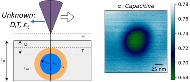
Knowing the dielectric properties of the interfacial region in polymer nanocomposites is critical to predicting and controlling dielectric properties. They are, however, difficult to characterize due to their nanoscale dimensions. Electrostatic force microscopy (EFM) provides a pathway to local dielectric property measurements, but extracting local dielectric permittivity in complex interphase geometries from EFM measurements remains a challenge. This paper demonstrates a combined EFM and machine learning (ML) approach to measuring interfacial permittivity in 50 nm silica particles in a PMMA matrix. We show that ML models trained to finite-element simulations of the electric field profile between the EFM tip and nanocomposite surface can accurately determine the interface permittivity of functionalized nanoparticles. It was found that for the particles with a polyaniline brush layer, the interfacial region was detectable (extrinsic interface). For bare silica particles, the intrinsic interface was detectable only in terms of having a slightly higher or lower permittivity. This approach fully accounts for the complex interplay of filler, matrix, and interface permittivity on the force gradients measured in EFM that are missed by previous semianalytic approaches, providing a pathway to quantify and design nanoscale interface dielectric properties in nanodielectric materials.
Keywords: electrostatic force microscopy, dielectric constant, polymer nanocomposites, finite-element analysis, machine learning
1. Introduction
The addition of nanoscale fillers to polymer dielectrics to create nanodielectrics results in materials with significantly improved dielectric breakdown strength, permittivity, and loss properties. For example, nanofillers can increase the effective dielectric permittivity without compromising, or in some cases even enhancing, the breakdown strength.1,2 Nanodielectrics are thus promising materials for applications in high voltage cable transmission, storage application, and solid state electronics.3,4 The enhancement in properties depends critically on the properties and volume of the interfacial region:5 a nanosized region surrounding the filler with properties different from both the particle and the matrix. It is thus imperative for materials design and control that the properties of the interfacial region be known and the impact of the nanofiller surface chemistry on those properties understood. However, the nanometer scale of the interphase falls below the spatial resolution of many experimental measurement techniques making quantitative characterization of interfacial properties a challenge. Electrostatic force microscopy (EFM) is a potential tool for quantifying the permittivity in small regions.
EFM is a scanning probe method based on atomic force microscopy (AFM), where the conductive tip is electrically biased, and the effect of electrostatic forces between the tip and sample is detected.6,7 EFM can be used to obtain information on various electrical properties of a surface, such as dielectric constant,8 surface-bound charge, and contact potential.6,7 Some relevant applications include detection of injected charges on conductive nanolayers9 and characterization of semiconductor devices and junctions.10
This works builds on the work of other groups. Sharma et al.11 studied the EFM phase shift signal in DC mode to quantify the permittivity of the interfacial region in a BaTiO3/epoxy nanocomposite system. Peng et al.12 detected a change in local permittivity in LDPE/TiO2 nanocomposites and attributed them to a modified interface. They combined experimental results with numerical simulation to quantify the interface permittivity in agglomerated nanoparticles. An elaborate effort to understand the sensitivity of EFM measurements for measuring interface permittivity prediction was performed by El Khoury et al.13 The effect of various parameters, such as tip geometry, dimensions of sample, and permittivities of constituent phases (matrix, nanoparticle, interfacial region) on the EFM signals were studied using finite-element simulations. The authors concluded that the particle-interface assembly could be approximated as a particle of similar global dimensions, with an effective apparent permittivity. Furthermore, based on the sensitivity of force gradients that can be detected from EFM experiments, detectability limits of the interfacial region in several standard nanodielectric configurations were studied. In general, the authors found that lower dielectric permittivity matrices, higher interfacial permittivities and thicknesses, and shallower nanoparticles make the interface more detectable.
In this paper, DC-EFM measurements to detect the dielectric properties of the interfacial region from well-dispersed nanoparticles from bulk nanocomposites are reported. These measurements were performed for two types of nanocomposite systems, designed to measure the dielectric permittivity of the extrinsic and intrinsic interfacial regions. A machine learning (ML) model previously developed by us14 was used to determine the interfacial permittivity and thickness of the two systems. Finally, the extracted values of interface parameters were verified using bulk dielectric spectroscopy measurements.
2. Methods
2.1. Particles
Colloidal silica nanoparticles of an average diameter of 50 nm were purchased from Nissan Inc. Two types of nanoparticles were prepared: (1) particles with grafted PMMA with a graft density of 0.34 chains/nm2 and a molecular weight of 120 000 g/mol, (2) particles with grafted polyaniline acrylate polymer at a graft density of 0.34 chains/nm2 and a molecular weight of 134 000 g/mol.
To create the grafted polymers, poly(methyl methacrylate) (PMMA) and poly(acrylic acid N-hyroxysuccinimide) (PNAS) were synthesized by surface-initiated reversible addition-fragmentation chain transfer polymerization (SI-RAFT). The RAFT agent was 2-(dodecylthiocarbonothioylthio) propanoic acid (DoPAT). All chemicals were used as received unless otherwise specified. Methyl methacrylate (MMA, 99%, Acros) was purified by filtration through an activated basic alumina column. Azobisisobutyronitrile (AIBN) was recrystallized from methanol before use. Molecular weights and dispersity were determined by monitoring monomer conversion through 1H NMR and gel permeation chromatography (GPC). THF was used as the eluent for GPC at 30 °C and a flow rate of 1.0 mL/min. GPC was calibrated with poly(methyl methacrylate) (PMMA) standards obtained from Polymer Laboratories.
To synthesize free polyaniline acrylate, DoPAT (5 mg, 0.014 mmol), NAS (0.482 g, 2.84 mmol), and AIBN (140 μL in 0.01 M solution) were dispersed in 4.75 mL of DMF and transferred into a dried Schlenk flask. The mixture was degassed by three freeze–pump–thaw cycles, back-filled with nitrogen, and then placed in an oil bath at 65 °C. The polymerization solution was quenched in an ice bath and exposed to air after 24 h. The polymer solution was precipitated into diethyl ether and centrifuged at 6000 rpm for 5 min. The dispersion-precipitation process was repeated four times. The polymer was then redissolved in 5 mL of DMF and sparged with nitrogen for 15 min. N-Phenyl-p-phenylenediamine (1.05 g, 5.6 mmol) was dissolved in 2 mL of DMF. The solution was then added to the polymer solution where it was then transferred to an oil bath at 110 °C for 24 h. The polymerization was quenched in an ice bath and precipitated into diethyl ether and centrifuged at 6000 rpm for 5 min. The polymer was then dissolved in THF, and the dispersion-precipitation process was repeated until the supernatant was colorless. Polyaniline-acrylate-grafted NPs were synthesized by a surface-initiated reversible addition-fragmentation chain transfer polymerization (SI-RAFT).15 A typical polyaniline-acrylate-grafted NP synthesis was: DoPAT-NP (0.05 g, σ = 0.34 chains/nm2), NAS (0.30 g, 1.77 mmol), and AIBN (18 μL in a 0.1 M solution) were dispersed in 5 mL of DMF and transferred to a Schlenk flask. The remaining procedure is identical to the free polyaniline acrylate synthesis.
PMMA-Grafted NP Synthesis
Poly(methyl methacrylate) (PMMA)-grafted NPs were synthesized by surface-initiated reversible addition-fragmentation chain transfer polymerization (SI-RAFT).16
SEM images were used to estimate the size of the polyaniline-acrylate-grafted silica nanoparticles before dispersing them in the PMMA matrix. A thickness of 17.5 nm for the interfacial region was estimated by comparing the diameters of grafted nanoparticles from EFM measurements with bare particle SEM size.
2.2. Composites
Modified nanoparticles and PMMA were mixed well in a THF solution and precipitated by adding a small amount of DI water. The solvent was removed in a rotoevaporator under vacuum, 70 °C, and rotating at a speed of 100 RPM. The resulting mixture of polymer powder and grafted nanoparticles was dried in a vacuum oven at 80 °C for 12 h to remove any remnant solvent. The nanoparticle loading was tested using thermogravimetry, and the requisite amount of PMMA powder was then added to achieve a loading of about 1.5 weight percent. The resulting powder mixtures were melt mixed in a Thermo Haake Minilab Twin Screw Extruder at 190 °C and 100 rpm for 10 min.
2.3. EFM Samples
EFM measurements were performed on a silicon-based substrate. The wafers were coated with 50 nm of gold to create a conductive substrate surface. A silver paste was used to establish an electrical contact of the substrate with the EFM sample holders. The pure polymer samples were spin-coated from solution to form a 200 nm layer. For nanocomposites, thin sections of 200 nm were sliced using an ultramicrotome. These sections were deposited on marked Cu grids and were annealed at 70 °C for 2 h. Then, the annealed sections were imaged using TEM to identify well-dispersed regions followed by EFM measurements.
2.4. Characterization
TEM micrographs were used to quantify dispersion17 using a two-point correlation function. Using the Niblack algorithm, grayscale raw TEM images were converted to binary images, see Figure 1.18 The algorithm compares each pixel value to a threshold set by averaging user-defined window size pixels. Statistically representative volumes were then reproduced in COMSOL to predict the bulk permittivity based on the measured matrix, particle, and EFM measured interfacial permittivity to validate the EFM results.
Figure 1.
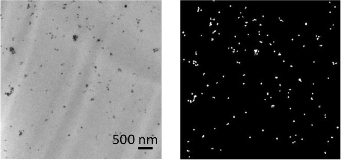
Example of TEM image binarization to quanitfy dispersion in a SiO2-PMMA nanocomposite.
Bulk dielectric spectroscopy measurements were taken on disc-shaped samples 400 μm thick, hot-pressed using a Carver Hot Press. The upper surface of the disc was sputter-coated with gold (of thickness 3 nm) to ensure a good electrical connection with the electrode. Samples were dried at 100 °C for at least 4 h to remove adsorbed moisture. Samples were tested in a Novocontrol Alpha Impedance Analyzer by applying a 1 V sinusoidal signal.
2.5. Electrostatic Force Microscopy (EFM)
The workflow required to obtain the interface permittivity required several steps. We provide an overview here followed by details.
EFM images were collected at several applied potentials V for the same region of the sample on particles protruding from the surface. The topography was used to calculate the size of the particle and its submersion depth in the composite.
The dependence of the measured EFM phase shift δϕ at each spatial location was used to extract the quadratic coefficient (with respect to V) of the force gradient dF/dz.
A large data set of simulated force gradients using finite-element solutions of the Poisson equation for the potential applied between the tip and a single nanoparticle within a polymer matrix were generated. All known parameters such as nanoparticle radius and permittivity of the filler and matrix were constrained to their known values, while unknown parameters such as interface thickness and permittivity were sampled to cover a range of possible values.
A machine learning (ML) model14 was fit to this data set to predict interface thickness and permittivity, given the force gradient profile along a line scan passing above the center of the nanoparticle as the features (input) to the model.
The ML model, which was trained to the simulated data set, was applied to the experimental force gradient data to extract the interface permittivity from the experimental data.
EFM measurements were performed with a commercial AFM (Cypher Asylum). The probe consists of metal-covered tips (Budget Sensors: ElectriMulti75-G and HQNSC18/Pt) supported by a cantilever, electrically connected to a metallic sample holder, and biased at an electrical potential. Because a precise value for tip size is essential for quantifying electrostatic force gradients, we independently calibrated the tip. Two fitting parameters are generally used to model a tip: the tip apex radius, Rapex, and the half an gle of the cone, θ, and there are several potential approaches.19,20 Similar to Fumagalli et al.,21 the capacitive force gradient was measured at various lift heights, z, for a gold-coated steel substrate. The results were fitted to the analytical equation:
| 1 |
Based on that fitting, we calculated θ = 12° and Rapex = 29 nm, which correspond well with the manufacturer’s claim of a 25 nm tip radius and side angle of 12°.
EFM force gradient measurements were performed in a double-pass, also called double-scan, configuration.22 In the first scan of the double pass, the topography of the sample surface is generated by a tapping mode. In the second scan, the probe is electrically biased and is lifted to a certain height. The probe follows the topographic profile measured from the first scan to fix the tip–sample distances throughout the second scan. In addition, we used the topography scan to calculate the diameter of the particle being probed. All the particles probed were projecting from the surface. By fitting a sphere to a small section of the particle profile, both the particle size and the depth of its center inside the sample surface were determined. The measured diameters of the embedded particles (±1 nm) studied are tabulated in Table 1. The estimated diameters were found to be consistent with the size of grafted silica nanoparticles.
Table 1. Radius and Protrusion Distance for Isolated Particles Estimated from Topography Measurements.
| Configuration | R | d |
|---|---|---|
| PANI-modified Particle 1 | 46 nm | 18 nm |
| PANI-modified Particle 2 | 43 nm | 12 nm |
| PANI-modified Particle 3 | 55 nm | 10 nm |
| PMMA-modified Particle 1 | 35 nm | N/A |
| PMMA-modified Particle 2 | 48 nm | N/A |
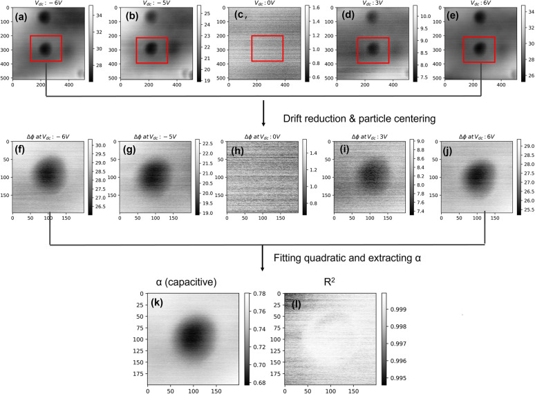
Figure 2 represents
raw phase shift images generated from EFM measurement at different
applied dc voltages over a nanoparticle-interface region. The probed
region is 1 by 1 μm. The electrostatic force can be extracted
from the raw phase shift image using the relation  where Q = 260
and k = 3 N/m represent the quality factor and spring
constant
of the probe respectively, and Fdc is the electrostatic force. The electrostatic force can be
expressed as a quadratic of applied voltage, Vdc:19
| 2 |
| 3 |
| 4 |
where Vcp is the work function between the tip and the sample, and C″ is the second derivative of probe-sample capacitance with respect to lift height z. While all coefficients, α, β, and γ, depend on the interface dielectric properties, the quadratic coefficient α depends solely on the capacitive contribution (C″) and enables accurately extracting the interface permittivity. In contrast, β and γ also depend on surface charges and contact potential, which can vary spatially and are generally unknown, making it difficult to extract interface permittivity from those terms.
Figure 2.
(a–e) EFM phase shift images at generated at different applied voltages at a lift height of 20nm. (f–j) Centered phase shift image after drift removal. Phase shift signal at each pixel was collected for five different voltages, and a quadratic was fitted to get α. (k) The α image isolating the capacitive contribution from phase shift signals. (l) Correlation coefficient image showing a good fit for all pixels.
In this study, phase shifts image were generated for the same nanoparticle-interface-matrix assembly for at least four different applied voltages (predominantly −3, −6, 0, 3 V). Each image was postprocessed to remove the spatial drift by aligning the particle centers). A 200 × 200 pixel region centered on the nanoparticle was selected from the image for each potential, and a quadratic fit was performed for the potential dependence at each pixel to extract α, β, and γ for each image. The accuracy of the fit parameters was estimated from the adjusted R2 values. An example of the spatial variation of α obtained at a lift height of 20 nm, along with the corresponding adjusted R2, are shown in Figure 2.
The phase images were produced using the following settings: setpoint of 0.5, free oscillation amplitude of 100 nm, and scan rate of 2.15 Hz. The setpoint is a measure of the amount of force applied on the surface. Lower setpoints result in larger applied force. The effect of lift height on the EFM signal around the particle center is plotted in Figure 3, which shows the extracted quadratic coefficient α along a line scan passing above the center of the nanoparticle.23
Figure 3.
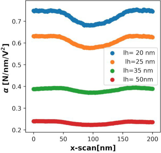
Profile of the quadratic coefficient α of EFM signal versus potential along a line scan passing above the particle center at multiple lift heights. The resolution decreases with increasing lift height.
3. Results
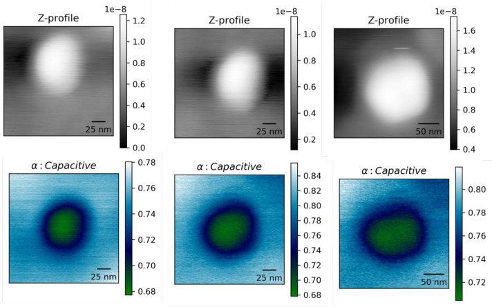
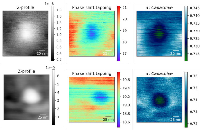
Figures 4 and 5 show the capacitive images for the PANI-modified and PMMA-modified nanocomposites. The alpha (capacitive) images were generated from the DC phase shift measurements. The line profile at the center of the nanoparticle shows a continuous hyperbolic profile (Figures 6 and 7). This effect is explained in ref (24). The presence of interface permittivity overshadows particle permittivity and can be treated as a singular component of effective dielectric permittivity. For the PMMA-modified nanoparticles, the contrast in the alpha profile decreases when compared to the polyaniline acrylate nanocomposite system because of the decreased permittivity of the interfacial region.
Figure 4.
Topography and alpha images for three different isolated particles for PANI-grafted nanocomposites. Alpha isolates the capacitive contribution from raw phase shift images. A line profile across the particle center (horizontal line centered vertically on the particle) is used to predict the interfacial parameters.
Figure 5.
Height, phase shift, and alpha (capacitive) image for a single isolated particle in PMMA-grafted nanocomposites. Note the narrower scale used for these samples required due to the smaller change in interfacial permittivity.
Figure 6.
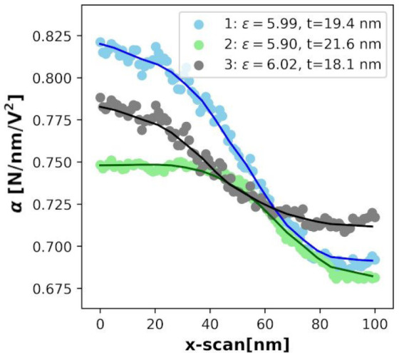
Comparison of the simulated (dotted) vs experimental alpha profile for the predicted interfacial parameters obtained from the ML model for PANI-grafted nanocomposites. The predicted parameters match the experimental profile with the simulated profile with high accuracy.
Figure 7.
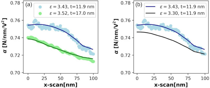
(a) Comparison of the simulated (lines) vs experimental (points) alpha profile for the predicted interfacial parameters obtained from the ML model for intrinsic interfaces in the PMMA-grafted nanocomposites. (b) Comparison of profiles with and without an interfacial layer.
As shown in Figure 8, the force gradient at the particle center decreases by increasing the protrusion height, d, from the sample surface. This is because of topography cross-talk:25 as the interelectrode distance (the total distance between the bottom and top electrode) increases, the effective signal decreases. Since the particle protrudes from the surface, the effective electrode distance increases to keep a constant lift height, decreasing the intensity of the force gradients.
Figure 8.
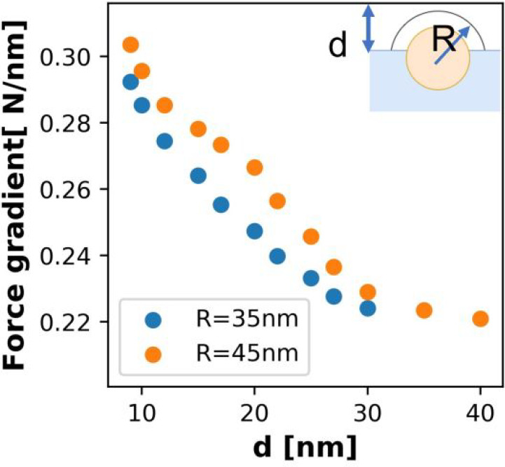
Simulated force gradient for unit applied potential at particle center vs particle height from surface (d) decreases because interelectrode distance increases.
Figure 9 represents a schematic of the two possible geometric setups of the nanoparticle with the exposed interfacial region. The interfacial region and nanoparticle protrude from the surface, or a bare particle is exposed, leaving an interfacial shell on the surface. We compared the force gradient profiles for the two different geometric setups from COMSOL finite-element simulations of the Poisson equation for electric potential applied between the tip and sample of each geometry (simulations outlined in the next section with further details in ref (14)). A constant lift height was ensured while simulating the tip’s motion across the exposed particle surface. A minor change in force gradient profile was measured for the two geometric combinations across the nanoparticle. The polymer brushes were “grafted from” the silica surface and hence are covalently bonded and difficult to cleave from the particle surface during sample preparation. Therefore, geometric setup 1 was used to model particles with exposed geometry.
Figure 9.
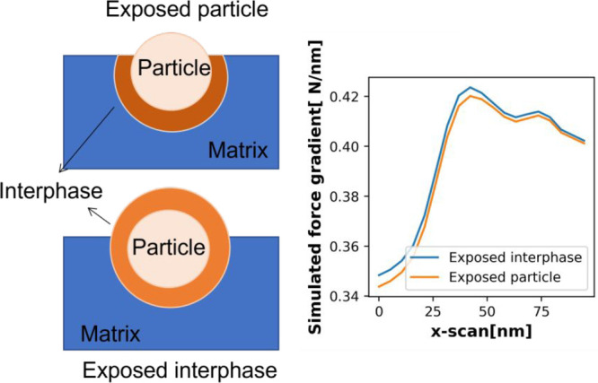
Comparing simulated force gradients at unit applied potential generated from two geometric configurations for R = 55 nm and ∈interfacial = 3.
As reported in ref (14), the data set to train a machine learning model to predict interface permittivity from force gradient profiles as inputs was generated from numerical simulations of the Poisson equation for electric potential between the EFM tip and sample performed in COMSOL. We briefly outline the simulations and ML protocol here; please see ref (14) for further details. The data set was generated by varying experimental unknowns (interface permittivity and thickness) and fixing the known experimental parameters, such as polymer matrix permittivity, nanoparticle size, and permittivity.
The known experimental parameters were carefully measured from independent experiments to simulate the EFM experimental conditions in COMSOL accurately. The static permittivity of the pure matrix was estimated from the EFM measurements. A similar capacitive force gradient was measured at multiple lift heights for a 200 nm thick PMMA film and was fitted to an analytical equation given by:
 |
5 |
where h and ϵr are the thickness and permittivity of the film, and all remaining quantities are the same as in eq 1. Riedel26 used the equation to measure the dielectric permittivity of a layer of SiO2 with 5% error. The measured permittivity for PMMA of 3.28 from EFM matches well results from dielectric spectroscopy measurements of bulk PMMA.
For each combination of unknown experimental parameters, we simulated the Poisson equation for the electric potential between the tip and the sample for unit applied potential, for various positions of the tip relative to the center of the nanoparticle. For each position, we predicted the force F on the tip due to the applied unit potential, which yields the quadratic coefficient of the force with respect to the applied potential (as extracted from the experiment above). Finally, for each position, 14, the force gradient at a specific lift height, l, was generated from the finite difference derivative of the force scans generated at two lift heights, l – δ and l + δ, where l is the lift height, with δ chosen between 2 and 5 nm to balance errors in subtraction of simulations (small δ) versus nonlinearity errors (large δ). See ref (14) for further details on the finite-element simulations to calculate the force gradient profiles
3.1. ML to Predict Interfacial Properties
The data set for training the ML models was constructed using the simulations as outlined above for 100 pairs of permittivity and thickness uniformly sampled within a range of expected experimental values as shown in Figure 10. Force gradient scans across the particle center were generated for each parameter combination and three different particle geometries. The particle geometries were based on the topography of the three nanoparticles, across which the alpha (capacitive) profile was experimentally measured. ML models were trained on each data set to predict the interfacial parameters, given the force gradient profile (α profile from the experiment) as input. Specifically, we trained support vector regression (SVR) models with all hyperparameters optimized using a grid search to maximize cross-validation scores within a training set and then evaluated on an independent test set, using an 80–20 train-test split of the overall data set. See ref (14) for further details on the setup and validation of the ML models and the Supporting Information for the complete data sets and Python notebooks to evaluate and apply these models.
Figure 10.
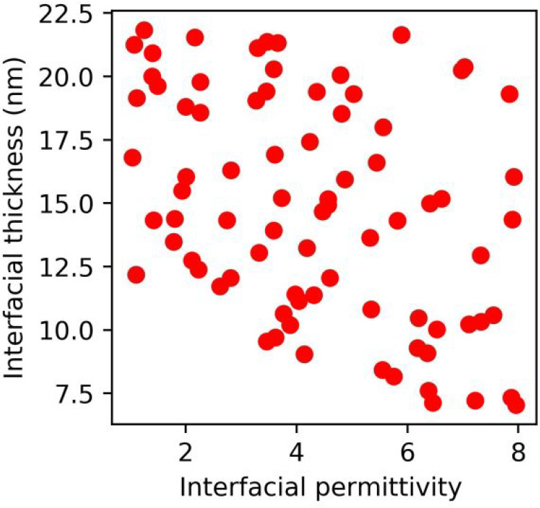
Sampling of the unknown interfacial parameters used to generate the force gradient data set.
Table 2 shows the ability of the ML model to predict the interface parameters based on numerical data. The interfacial permittivity is estimated with higher accuracy for an exposed nanoparticle than buried particles. This is because the force gradient contrast (difference in force gradient at the top of the particle with respect to the matrix) increases dramatically for particles with exposed geometry. Hence, the accuracy of ML models to predict the interfacial permittivity improves as particles with exposed interfaces protrude for the sample surface.
Table 2. Performance of ML Model on the Various Trained Data Setsq.
| Model | CV score | MAE (train) | MAE (test) |
|---|---|---|---|
| SVR(IP) PANI-modified Particle 1 | 92.1 | 0.11 | 0.19 |
| SVR(IP) PANI-modified Particle 1 | 93.5 | 0.09 | 0.19 |
| SVR(IP) PANI-modified Particle 1 | 92.3 | 0.10 | 0.20 |
| SVR(t) PANI-modified Particle 1 | 66.1 | 1.11 nm | 1.95 nm |
| SVR(t) PANI-modified Particle 2 | 61.5 | 1.41 nm | 2.2 nm |
| SVR(t) PANI-modified Particle 3 | 63.3 | 1.32 nm | 1.92 nm |
SVR(IP) particle 1 represents a support vector machine for interfacial permittivity measurements on the geometric configuration of particle 1 with (t) indicating interface thickness. MAE is mean absolute error, and CV is average correlation score.
ML models (SVR(t) PANI-modified Particle 1) also predict the interfacial region’s thickness with high accuracy when particle depth is known as expected based on simulated measurements in ref.14
3.2. Prediction of ML Model on the Experimental Data
The trained ML model was used to predict the interface parameters of each nanocomposite system from the experimental alpha (capacitive) measurements. The results of interfacial parameter predictions for three different PANI-modified nanoparticle profiles are shown in Figure 6. The interfacial permittivity is 5.95 ± 0.2 with a thickness of 19.3 ± 1.4 nm, which was estimated from the three experimental profiles measured against three isolated particles. The simulation profile generated for the predicted parameters matches the experimental data for the three different profiles.
As an independent validation, EFM measurements were done on a 200 nm thick spin-coated polyaniline acrylate film. A permittivity of 5.60 for polyaniline acrylate films was estimated from this measurement, which is similar to that determined for the PAN interfacial region surrounding the nanoparticle. In addition, the predicted thickness of 19 nm matches well with a brush size of 17 nm estimated from the size comparison of bare and grafted nanoparticles using SEM.
The results of interfacial parameter predictions for two PMMA-modified nanoparticle profiles are shown in Figure 7. The interfacial permittivities of 3.43 + 0.24 and 3.52 + 0.33 and thicknesses of 11.9 and 17 nm were predicted for the PMMA-modified particle experimental profiles. The thickness agrees well with independent work that measures brush thickness.27 However, we see a spread in the predicted parameters attributed to low sensitivity and high noise in the experimental data. The α images, in general, are noisy for the case of a PMMA-grafted nanoparticle system, in turn making the analyzed line profiles noisy. The predicted interfacial permittivity is very close to the permittivity of the matrix. The comparison of force gradient profiles with and without the interfacial layer is shown in the Figure 7b. The two profiles look very similar with a force gradient contrast difference of 0.001 nN/nm. This contrast is too low to be detectable from the EFM experiments. Nonetheless, although the confidence levels of the quantitative permittivity is low, it is clear that an intrinsic interface with permittivity higher than the matrix is observed for the PMMA-grafted nanocomposite system.
4. Discussion
To further validate these results, a two-dimensional finite-element model using the commercial software package COMSOL developed by Huang et al.28 was used to predict the bulk dielectric permittivity. Briefly, the filler dispersion was obtained from descriptor-based TEM image characterization (two-point correlation functions). A composite was built in COMSOL as a statistical volume element (SVE) consistent with the descriptors obtained from TEM. Triangular elements were used to capture the shape of the features with a refined mesh in the interfacial region. The lateral services were periodic, and an AC voltage was applied to the top of the sample, with the bottom grounded. The structure was regarded as a parallel plate capacitor. The effective dielectric constant of the composites was calculated using the following equation:
| 6 |
Here V* (ω) is the applied voltage as a function of angular frequency ω, and Jy*(ω) is the average complex AC current density along the direction perpendicular to the electrode and was measured at the grounded surface from the simulation output. d is the sample thickness, and ε0 is the vacuum permittivity as 8.85 × 10⁻¹² F/m.
Figure 11 shows an example SVE for a PAN-grafted composite. The clusters were modeled as ellipses. An interfacial permittivity of 5.9 and thickness of 20 nm was used to model a PAN-grafted nanocomposite system. The relative permittivities of 3.9 and 3.3 were used for the silica nanofiller and PMMA matrix. A very low electrical conductivity value of 10–1 S/m was used for all three components.
Figure 11.
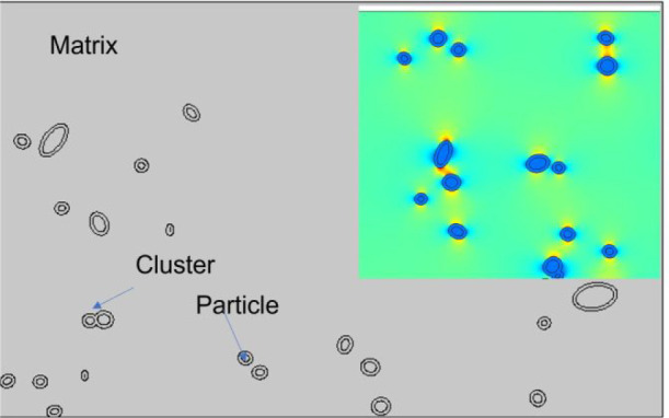
A representative volume element for a PAN-grafted system generated using a microstructural reconstruction tool. (inset) Electric field intensity distribution.
The results of simulated and experimental bulk dielectric permittivity at 0.01 Hz are shown in Table 3. We show that combining EFM results with finite-element model can predict the bulk dielectric response of nanocomposites. The predicted bulk permittivity of 3.54 for a PAN-grafted system and 3.36 for a PMMA-grafted system at 0.01 Hz matches well with the experimental results (of 3.64 and 3.37 respectively). A prediction within 0.1 permittivity supports the validity of this approach and these results.
Table 3. Comparing Simulated Bulk Permittivity Measurements with the Experimental Permittivity at 0.01 Hz.
| System | Interfacial permittivity | Bulk permittivity (simulation) | Bulk permittivity (experiment) |
|---|---|---|---|
| PAN-grafted | 5.90 | 3.54 | 3.64 |
| PMMA-grafted | 3.50 | 3.33 | 3.37 |
5. Summary
We have established a methodology to measure the interfacial permittivity in nanodielectrics from EFM measurements, leveraging ML models to avoid implifying assumptions. Capacitive profiles from raw phase shift images were generated for a single isolated particle dispersed in the matrix. Simultaneously, a ML model was trained on a numerical data set to predict a given geometry’s interfacial permittivity and thickness. The trained model was used to predict the interface permittivity and thickness from the capacitive experimental profile.
Interfacial measurements were carried for two different grafted silica nanoparticles dispersed in PMMA. For a PAN-grafted composite, an interfacial region surrounding the nanoparticle is observed from EFM measurements. The dielectric permittivity and thickness of the interfacial region were quantified using the ML model with high accuracy as validated by independent measurements of the grafted brush thickness and the PAN permittivity. For PMMA-grafted composites, no prominent interfacial layer is seen in the EFM images, but an interfacial region of higher permittivity than the matrix was detected.
Acknowledgments
This material is based on the work supported by the National Science Foundation under Grant CMMI 1729452. All calculations were carried out at the Center for Computational Innovations at Rensselaer Polytechnic Institute. Special thanks to the L.C. Brinson research group and the W. Chen research group for fruitful discussions.
Data Availability Statement
All data and analysis code for the results presented above are included in the Supporting Information, along with additional details of the COMSOL simulations used for generating the data.
Supporting Information Available
The Supporting Information is available free of charge at https://pubs.acs.org/doi/10.1021/acsaelm.2c01331.
Data files: Height.csv: Topography data from AFM. EFM*V.csv (* = −6, −5, +0, +3, +6): EFM images at several potentials. InterfaceParams.csv: Random sampling of several interface permittivity and thickness. ForceGradients.csv: Simulated force gradient scans for each of these interface parameters. ForceGradientFit.csv: Simulated scan for interface parameters extracted from experiment. Analysis scripts and workflow: Topography.ipynb: Extracts nanoparticle size from AFM height data. AlphaFit.ipynb: Extracts capacitance profile from EFM images at several potentials. This generates Alpha.csv used in the ML analysis. ML_Analysis.ipynb: Fits ML models to predict InterfaceParams as targets using ForceGradients as features. Applies this to the experimental data to extract the interface permittivity and thickness of the experimental sample. Finally, it compares the measured force gradient scan with a simulated scan at the extracted parameters (ForceGradientFit) (ZIP)
The authors declare no competing financial interest.
Supplementary Material
References
- Schadler L. S.; Nelson J. K. Polymer Nanodielectrics – Short History and Future Perspective. J. Appl. Phys. 2020, 128 (12), 120902. 10.1063/5.0019865. [DOI] [Google Scholar]
- Tanaka T.; Vaughan A. S.. Tailoring of Nanocomposite Dielectrics; Jenny Stanford Publishing, 2016. [Google Scholar]
- Hildinger T.; Weidner J. R. Progress in development of a nanocomposite stator winding insulation system for improved generator performance. 2017 IEEE Electrical Insulation Conference (EIC) 2017, 139–142. 10.1109/EIC.2017.8004655. [DOI] [Google Scholar]
- Streibl M; Karmazin R.; Moos R. Materials and applications of polymer films for power capacitors with special respect to nanocomposites. IEEE Transactions on Dielectric and Electrical Insulation 2018, 25 (6), 2429. 10.1109/TDEI.2018.007392. [DOI] [Google Scholar]
- Smith R. C.; Nelson J. K.; Schadler L. S. Electrical behavior of particle filled polymer nanocomposites. Physical Properties of Polymer Nanocomposites 2010, 70. 10.1533/9780857090249.1.70. [DOI] [Google Scholar]
- Kumar B.; Crittenden S. R. Nanoscale dielectric measurements from electrostatic force microscopy. Modern Physics Letters B 2014, 28 (24), 1430011. 10.1142/S0217984914300117. [DOI] [Google Scholar]
- Melitz W.; Shen J.; Kummel A. C.; Lee S. Kelvin probe force microscopy and its application. Surface Science Reports 2011, 66, 1–27. 10.1016/j.surfrep.2010.10.001. [DOI] [Google Scholar]
- Hou Y.; Wang G.; Ma C.; Feng Z.; Chen Y.; Filleter T. Quantification of the dielectric constant of MoS2 and WSe2 Nanosheets by electrostatic force microscopy. Materials Characterization 2022, 193, 112313. 10.1016/j.matchar.2022.112313. [DOI] [Google Scholar]
- Verdaguer A.; Cardellach M.; Segura J. J.; Sacha G. M.; Moser J.; Zdrojek M.; Bachtold A.; Fraxedas J. Charging and discharging of graphene in ambient conditions studied with scanning probe microscopy. Appl. Phys. Lett. 2009, 94, 233105. 10.1063/1.3149770. [DOI] [Google Scholar]
- Nakagiri N.; Yamamoto T.; Sugimura H.; Suzuki Y.; Miyashita M.; Watanabe S. Application of scanning capacitance microscopy to semiconductor devices. Nanotechnology 1997, 8, A32. 10.1088/0957-4484/8/3A/007. [DOI] [Google Scholar]
- Sharma A.; Basu S.; Gupta N. Investigation of the interface in nanodielectrics using electrostatic force microscopy. IEEE Transactions on Dielectrics and Electrical Insulation 2020, 27, 433–441. 10.1109/TDEI.2019.008435. [DOI] [Google Scholar]
- Peng S.; Zeng Q.; Yang X.; Hu J.; Qiu X.; He J. Local Dielectric Property Detection of the Interface between Nanoparticle and Polymer in Nanocomposite Dielectrics. Scientific Reports 2016, 6, 38978. 10.1038/srep38978. [DOI] [PMC free article] [PubMed] [Google Scholar]
- El Khoury D.; Arinero R.; Laurentie J. C.; Castellon J.; Frechette M. Investigation of EFM capabilities for probing interphases in nanodielectric materials: A numerical study. 2016 IEEE Int. Conf. Dielectr. (ICD) 2016, 800–803. 10.1109/ICD.2016.7547737. [DOI] [Google Scholar]
- Gupta P.; Schadler L. S.; Sundararaman R. Dielectric properties of polymer nanocomposite interphases from electrostatic force microscopy using machine learning. Materials Characterization 2021, 173, 110909. 10.1016/j.matchar.2021.110909. [DOI] [PMC free article] [PubMed] [Google Scholar]
- Bilchak C.; Buenning E.; Asai M.; Zhang K.; Durning C. J.; Kumar S. K.; Huang Y.; Benicewicz B. C.; Gidley D. W.; Cheng S.; Sokolov A. P.; Minelli M.; Doghieri F. Polymer-Grafted Nanoparticle Membranes with Controllable Free Volume. Macromolecules. Macromolecules 2017, 50 (18), 7111–7120. 10.1021/acs.macromol.7b01428. [DOI] [Google Scholar]
- Li C.; Han J.; Ryu C. Y.; Benicewicz B. C. A versatile method to prepare RAFT agent anchored substrates and the preparation of PMMA grafted nanoparticles. Macromolecules 2006, 39 (9), 3175–3183. 10.1021/ma051983t. [DOI] [Google Scholar]
- Xu H.; Li Y.; Brinson L. S.; Chen W. A Descriptor-Based Design Methodology for Developing Heterogeneous Microstructural Materials System. Journal of Mechanical Design 2014, 136, 051007. 10.1115/1.4026649. [DOI] [Google Scholar]
- Niblack W.An Introduction to Digital Image Processing; Prentice-Hall: Englewood Cliffs, NJ, USA, 1986. [Google Scholar]
- El Khoury D.; Arinero R.; Laurentie J.; Bechelany M.; Ramonda M.; Castellon J. Electrostatic force microscopy for the accurate characterization of interphases in nanocomposites. J. Nanotechnology 2018, 9, 2999–3012. 10.3762/bjnano.9.279. [DOI] [PMC free article] [PubMed] [Google Scholar]
- Passeri D.; Bettucci A.; Germano M.; Rossi M.; Alippi A.; Orlanducci S.; Terranova M.; Ciavarella M. Effect of tip geometry on local indentation modulus measurement via atomic force acoustic microscopy technique. Rev. Sci. Instrum. 2005, 76, 093904. 10.1063/1.2044607. [DOI] [Google Scholar]
- Fumagalli L.; Esteban-Ferrer D.; Cuervo A.; Carrascosa J. L.; Gomila G. Label-free identification of single dielectric nanoparticles and viruses with ultraweak polarization forces. Nat. Mater. 2012, 11, 808–816. 10.1038/nmat3369. [DOI] [PubMed] [Google Scholar]
- Portes L.; Girard P.; Arinero R.; Ramonda M. Force gradient detection under vacuum on the basis of a double pass method. Rev. Sci. Instrum. 2006, 77, 096101. 10.1063/1.2336104. [DOI] [Google Scholar]
- Belaidi S.; Girard P.; Leveque G. Electrostatic forces acting on the tip in atomic force microscopy: Modelization and comparison with analytic expressions. J. Appl. Phys. 1997, 81, 1023–1030. 10.1063/1.363884. [DOI] [Google Scholar]
- Sacha G. M.; Sahagun E.; Sáenz J. J. A method for calculating capacitances and electrostatic forces in atomic force microscopy. J. Appl. Phys. 2007, 101 (2), 024310. 10.1063/1.2424524. [DOI] [Google Scholar]
- Van der Hofstadt M.; Fabregas R.; Biagi M. C.; Fumagalli L.; Gomila G. Nanoscale dielectric microscopy of non-planar samples by lift-mode electrostatic force microscopy. Nanotechnology 2016, 27, 405706. 10.1088/0957-4484/27/40/405706. [DOI] [PubMed] [Google Scholar]
- Riedel C.Dielectric and Mechanical Properties of Polymers at Macro and Nanoscale. Ph.D. Thesis, Universite Montpellier II, 2010. [Google Scholar]
- Dukes D.; Li Y.; Lewis S.; Benicewicz B. C.; Schadler L. S.; Kumar S. Conformational Transitions of Spherical Polymer Brushes: Synthesis, Characterization, and Theory. Macromolecules 2010, 43 (3), 1564–1570. 10.1021/ma901228t. [DOI] [Google Scholar]
- Huang Y.; Krentz T. M.; Nelson J. K.; Schadler L. S.; Li Y.; Zhao H.; Brinson L. C.; Bell M.; Benicewicz B. C.; Wu K.; Breneman C. M. Prediction of interface dielectric relaxations in bimodal brush functionalized epoxy nanodielectrics by finite element analysis method. 2014 IEEE Conference on Electrical Insulation and Dielectric Phenomena (CEIDP) 2014, 748–751. 10.1109/CEIDP.2014.6995897. [DOI] [Google Scholar]
Associated Data
This section collects any data citations, data availability statements, or supplementary materials included in this article.
Supplementary Materials
Data Availability Statement
All data and analysis code for the results presented above are included in the Supporting Information, along with additional details of the COMSOL simulations used for generating the data.


