Abstract
Topological insulators are electronic materials with an insulating bulk and conducting surface. However, due to free carriers in the bulk, the properties of the metallic surface are difficult to detect and characterize in most topological insulator materials. Recently, a new topological insulator Bi1.5Sb0.5Te1.7Se1.3 (BSTS) was found, showing high bulk resistivities of 1–10 Ω.cm and greater contrast between the bulk and surface resistivities compared to other Bi-based topological insulators. Using Terahertz Time-Domain Spectroscopy (THz-TDS), we present complex conductivity of BSTS single crystals, disentangling the surface and bulk contributions. We find that the Drude spectral weight is 1–2 orders of magnitude smaller than in other Bi-based topological insulators, and similar to that of Bi2Se3 thin films, suggesting a significant contribution of the topological surface states to the conductivity of the BSTS sample. Moreover, an impurity band is present about 30 meV below the Fermi level, and the surface and bulk carrier densities agree with those obtained from transport data. Furthermore, from the surface Drude contribution, we obtain a ~98% transmission through one surface layer — this is consistent with the transmission through single-layer or bilayer graphene, which shares a common Dirac-cone feature in the band structure.
The special features of a topological insulator — insulating bulk and conducting surface1,2, have been attributed to the presence of time-reversal symmetry and spin-orbit interaction2,3. Earlier-discovered three-dimensional topological insulators such as Bi2Se3, Bi2Te3 and Sb2Te3 have a high concentration of bulk carriers, resulting in a weakly-insulating bulk electronic state and making it difficult to detect the metallic surface states4,5,6,7. In BSTS8,9, non-stoichiometry-induced donors and acceptors compensate each other, yielding high bulk resistivities of 1–10 Ω.cm and high contribution (~70%) of the total conductance by surface transport, thus showing a greater contrast between the bulk and surface resistivities compared to Bi2Se3, Bi2Te3 and even Bi2Te2Se10. THz-TDS is a non-contact far-infrared optical technique suitable for probing the low-energy excitations of strongly correlated electronic systems such as cuprate superconductors11, pnictide superconductors12, and colossal magnetoresistance manganites11. In this Report, we present the temperature-dependent optical conductivity of BSTS samples at temperatures 5–150 K in the far-infrared regime (0.4–3.0 THz). By modeling the total conductance as the sum of Drude and Lorentz components, we were able to obtain a Drude weight to be 1–2 orders of magnitude smaller than other Bi-based topological insulators10, and close to the value for the surface state of Bi2Se3 thin films13. This suggests a significant contribution of the topological surface states to the conductivity of the BSTS sample.
Results
Sample growth, electronic transport and ARPES
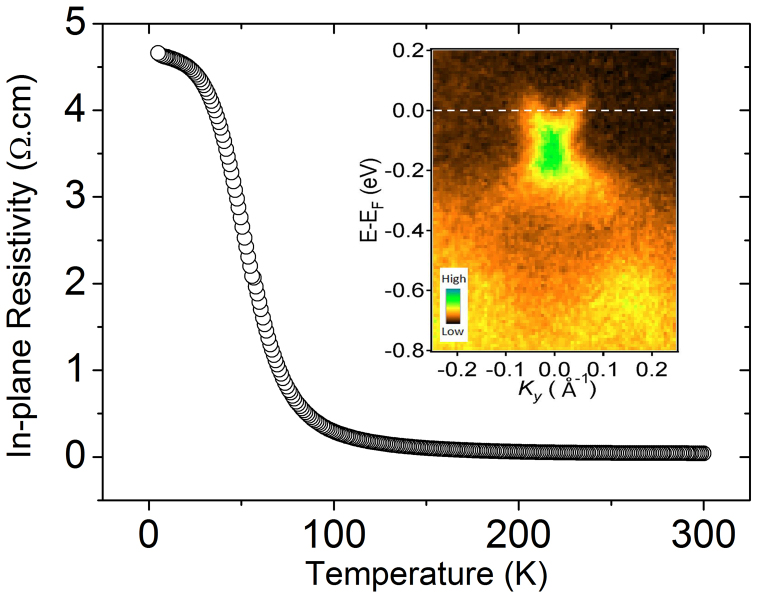
Samples were grown by the modified Bridgeman method (Methods section)14. In-plane DC resistivity data were taken using a Quantum Design Physical Property Measurement System (PPMS), as shown in Fig. 1. Both the temperature dependence and the absolute values of resistivity are consistent with those in Ref. 9. Scanning Electron Microscopy with Energy Dispersive X-ray spectroscopy (SEM-EDX) data of the BSTS samples were reported in Ref. 14, giving the chemical composition of the sample, and consistent with previous publications8,9. Evidences for two-dimensional surface properties in our samples were given by ambipolar14, as well as angle-resolved photoemission spectroscopy (ARPES) data. The inset of Fig. 1 shows ARPES data of Bi1.5Sb0.5Te1.8Se1.2 single crystals obtained from a Scienta R4000 electron analyzer at the Surface, Interface and Nanostructure (SINS) beamline at Singapore Synchrotron Light Source (SSLS) (Methods section). The data show the surface state at the vicinity of Γ point, which is an important signature of a sample being a topological insulator. The observed surface state does have a similar feature to that in a previous report of ARPES on Bi1.5Sb0.5Te1.7Se1.315. Note that, due to the limited energy resolution, many detailed structures are unresolved at this stage. In this Report we focus on the optical properties in the THz regime.
Figure 1. In-plane DC resistivity.
Inset = ARPES data of BSTS single crystal. Notice the band dispersion near the Fermi level.
THz-TDS
Details of the THz-TDS setup are given in the Methods section. By finding the ratio between the sample  and reference
  spectra, one is able to obtain the complex transmittance,
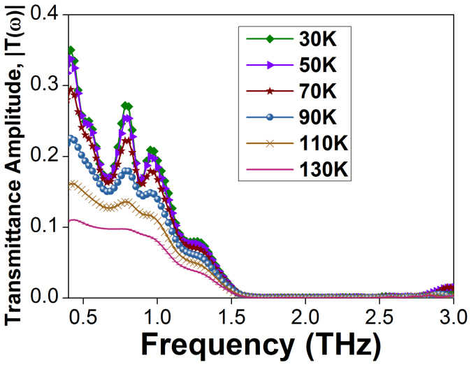
  . Figure 2 shows the amplitude of the experimental transmittance of BSTS,
  , at various temperatures. A periodicity due to multiple reflections within the sample is observed at low temperatures and gets washed out with increasing temperature above ~100 K. We account for these reflections in Eq. (1) below when we extract the optical conductivity. In addition, a drop in
  to zero has been observed at ~1.7 THz and after which, rises again at ~2.8 THz. This corresponds to an optical phonon mode at 1.9 THz, to be described later. By fitting the experimental
  to the theoretical expression
 |
one is able to obtain the complex refractive index of the sample,  . Here d ( = 60 μm) is the sample thickness, c is the speed of light in vacuum, and the summation in Eq. (1) accounts for multiple reflections of the THz pulse inside the sample, with the number of reflections M = 6. Note that, due to the considerable thickness of the sample, we could not assume infinite reflections of the THz pulse inside the sample, as was usually assumed for nanometer-thickness thin films.
Figure 2. Amplitude of complex transmittance,  , at various temperatures.
Drude-Lorentz model
The complex refractive index is then used to calculate the complex conductivity  , where
  and
and  ,
,  being the permittivity of free space, and
  the high-frequency dielectric constant. As an unknown quantity,
  was initially set to 1 when we calculate the experimental conductance, via the expression
  (tbulk = 60 μm); then it will be used as a fitting parameter14 in the conductance fitting for each temperature. We model the conductance to contain a Drude (D) free-carrier contribution averaged over the surface and bulk, and a Lorentz (L) contribution from the insulating bulk, similar to the analysis carried out for Bi2Se314 and given by
  , where
 |
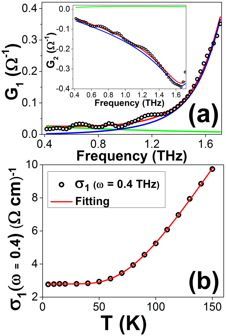
The fitting parameters ωpD and γD denote the plasma frequency and scattering rate of the Drude component, respectively. ωpL, ωoL and γL are the plasma frequency, oscillator frequency and the scattering rate of the Lorentz component, respectively. The temperature dependence of these fitting parameters will be discussed later. Figure 3(a) shows the real and imaginary components of the experimental complex conductance  of the sample at 30 K, alongside the fit to the Drude-Lorentz model, and the respective Drude and Lorentz contributions. Compared to other Bi-based topological insulators10, the low-frequency response of our BSTS sample is Lorentz-like with a very small Drude offset (see Fig. 3(a)). This is consistent with our BSTS sample having a large bulk resistivity.
Figure 3.
(a) Real conductance G1(ω) at 30 K. Inset shows the imaginary conductance G1(ω). (O) = data. Solid lines = Drude (green) and Lorentz (blue) contributions, and the fit to data (red). (b) Low-frequency real conductivity σ1 versus temperature. (O) = data. Solid line = fit to Eq. (3).
We estimate how dc conductivity of BSTS varies with temperature by plotting the low-frequency σ1 (ω = 0.4 THz) versus temperature, then fitting it to the thermally-activated hopping model given by16
 |
from 5 K to 150 K, where A is a constant, D is a nonzero offset at 0 K, Δ is the activation energy, and kB is the Boltzmann constant. Figure 3(b) shows the low-frequency conductivity together with the fit to Eq. (3), with D = (2.80 ± 0.01) (Ω.cm)−1, and activation energy Δ = (26.7 ± 0.2) meV. The fitted value of Δ is consistent with the results by Ren et al. that vary between 22 and 53 meV17. A similar energy scale of 30–40 meV has also been found in Bi2Te2Se, which has been attributed to transitions from the impurity bound states to the electronic continuum10.
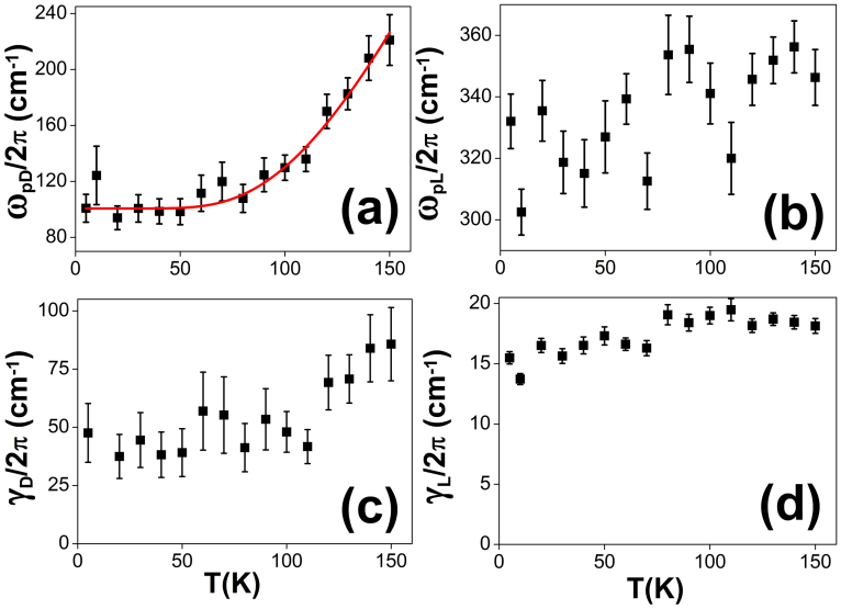
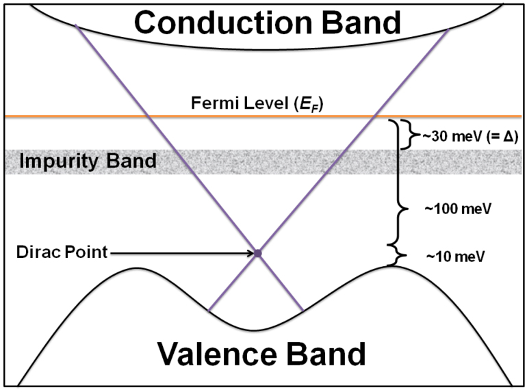
We next discuss factors that contribute to the frequency and temperature dependence of the surface and bulk conductance, by looking at the temperature dependence of the fitting parameters in Eq. (2). Figures 4(a) and (b) display the temperature-dependent Drude plasma frequency (ωpD) and Lorentz plasma frequency (ωpL) respectively, while Figs. 4(c) and (d) show the Drude (γD) and Lorentz (γL) scattering rates respectively. First note that the absolute values of these fitting parameters are consistent with those obtained for Bi2Se3 thin films13,18. We found ωpD to increase significantly with temperature, while γD (proportional to charge carrier mobility) shows marginal increase with temperature. As for bulk carrier dynamics, both ωpL and γL exhibit marginal correlation with temperature. Since the square of plasma frequency ωp, is directly proportional to the charge carrier density N via the relation  , where e denotes the elementary charge and m* is the effective mass of the charge carrier, this suggests the increase in the surface charge density with temperature while the scattering rate changes only marginally. This is unlike the case of conventional metals, where the increase in resistivity with increasing temperature originates from the increase in scattering rate, with the charge density remaining temperature independent. The increase in surface charge carrier density may be due to the contribution of bulk carriers from the donor impurity band to the topological surface states (Fig. 5). This band, situated ~30 meV ( = activation gap Δ) below the Fermi level, starts to contribute carriers to the Dirac cone above 60 K, leading to a rise in the Drude spectral weight
  . This relationship between Δ and
  is supported by our fit of
  (in Fig. 4(a)) with Eq. (3) — a good fit was obtained with Δ = (31 ± 4) meV (solid line in Fig. 4(a)), consistent with the earlier-obtained value of Δ = (26.7 ± 0.2) meV from the σ(ω = 0.4 THz) fit. This is not surprising, since, from Eq. (2),
  . Figure 5 shows a schematic of the relative positions of the valence band, Dirac point, impurity band, chemical potential, and conduction band in BSTS — they are consistent with that obtained from transport data of BSTS with similar composition9. Note that in Ref. 9, though the Fermi level is pinned to the impurity band in the bulk, the impurity band bends downwards at the surface, such that the impurity band now lies below the Fermi level at the sample surface.
Figure 4. Temperature dependence of the (a) Drude plasma frequency ωpD, (b) Lorentz plasma frequency ωpL, (c) Drude scattering rate γD, and (d) Lorentz scattering rate γL.
Solid line = fit to Eq. (3).
Figure 5. Schematic of band diagram of BSTS, with the (donor) impurity band lying just below the Fermi level.
The relative positions of the valence band, Dirac point, Fermi level and conduction band were taken from Ref. 15 for a Bi1.5Sb0.5Te1.7Se1.3 sample. Δ = activation gap.
Drude spectral weight
In an optical conductivity study of a group of Bi-based topological insulators that does not include BSTS10, the far-infrared conductivity of its most compensated sample (Bi2Te2Se) is still affected by the extrinsic charge carriers due to non-stoichiometry and doping. In Ref. 10, in order to compare the charge densities due to the (a) topological surface states and (b) free (extrinsic) carriers in the bulk, the optical spectral weight was calculated using
 |
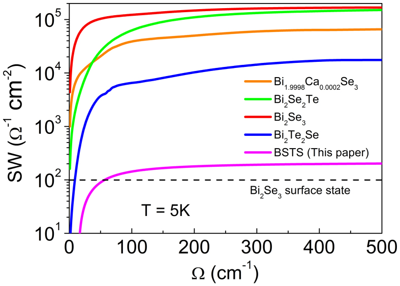
where the cutoff frequency, set at Ωmax = 500 cm−1, separates the low-frequency excitations from the interband transitions. We perform the same calculation for our BSTS sample using the Drude fitting parameters. Figure 6(a) displays the spectral weight of BSTS as a function of frequency, calculated at 5 K, and superposed with data from other Bi-based topological insulators from Ref. 10. The dashed line indicates the Drude spectral weight of Bi2Se3 thin films, which was attributed to the topological surface states13. We see that, compared to the spectral weights of other Bi-based topological insulators, the Drude spectral weight of our BSTS sample is one order of magnitude smaller than the most compensated sample — Bi2Te2Se, and is comparable to that of Bi2Se3 thin film. This is a clear indication that in BSTS, in comparison to other Bi-based topological insulator samples, the effect of the 3D bulk states is further suppressed, and the topological surface states could be more clearly resolved.
Figure 6. Spectral weight of various Bi-based topological insulators at 5 K calculated using Eq. 4.
Dashed line represents the contribution from topological surface carriers of Bi2Se3 thin film10,13. Adapted with permission from Fig. 4 of Ref. 10. Copyright 2012 by the American Physical Society.
Surface and bulk carrier density
Now that we have established the Drude component to have a significant two-dimensional surface contribution, we then re-express the experimental Drude conductance  in Eq. (2) as
 |
where the first term on the right-hand-side is the two-dimensional Drude conductance arising from a linear (Dirac-like) dispersion of the surface carriers19, with the factor 2 accounting for the top and bottom surfaces of the sample. The second term on the right-hand-side is the three-dimensional Drude conductance from the bulk carriers similar to Eq. (2), τ = 1/γD, Nsurf the surface electron density (of one surface), Nbulk the bulk electron density, νf = 6.0 × 10⁵ m/s the Fermi velocity9, and m* = 0.32me the electron effective mass9. By fitting the 10 K data to Eq. (7) from the 60-μm sample shown in Fig. 3, and another 90-μm sample shown in Fig. 7 later, we obtain two simultaneous equations in Nsurf and Nbulk, which are solved to give Nsurf = 3.8 × 1013 cm−2 and Nbulk = 1.7 × 1016 cm−3. We note that, though the obtained bulk carrier density is comparable to that obtained from transport measurements with Nbulk = 2.3 × 1016 cm−3 9, the surface carrier density is one order of magnitude larger than that from the transport measurements with Nsurf = 1.2 × 1012 cm−2 9. The origin of this discrepancy may come from the nature of optical techniques versus transport measurements. For a system like BSTS with impurity-induced inhomogeneity, the optical technique not only measures the carriers which directly scatter off impurities, but also free carriers which move back and forth within an area with a linear dimension determined by the mean free path. Both types of carriers contribute to an average Drude conductivity. On the other hand, in transport measurements, only the delocalized carriers throughout the whole region between two electrical contacts are measured. A similar reasoning has also been proposed for the optical study of phase-separated manganite thin films20. Scanning tunnelling microscopy of Bi2Se3 and Bi2Te3 revealed inhomogeneity of the local density of states on the surface near the Dirac point, due to charge disorder caused by bulk defects (“defect-induced charged puddles”)21. To lend further credence to the quality of our BSTS THz-TDS data, we note that the larger value of Nsurf from optical spectroscopy compared to transport measurements was also seen in Bi2Se3. For example, THz-TDS data on Bi2Se3 by Aguilar et al.13,18 obtained Nsurf ~ 2.1–3.3 × 1013 cm−2, which agrees with our data for BSTS (3.8 × 1013 cm−2). Transport data on Bi2Se3 yielded smaller values of Nsurf: 4.7 × 1012 cm−2 from Shubnikov de Haas (SdH) oscillations of single crystals22, and 7 × 1011 cm−2 from SdH oscillations of nanostructures23.
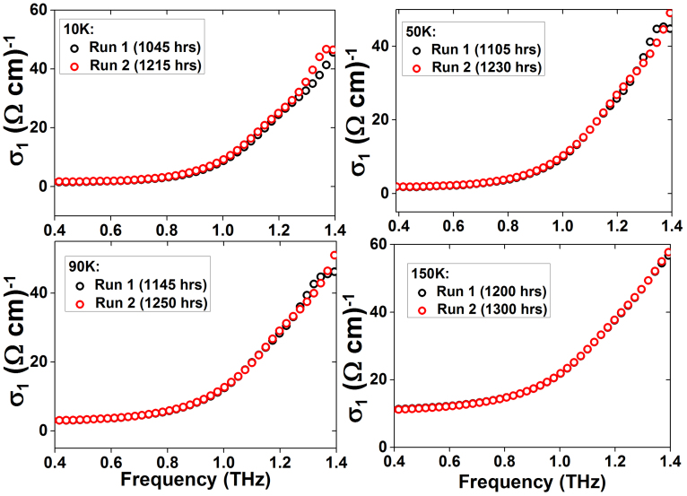
Figure 7. Real conductivity [σ1(ω)] of a 90-μm-thick BSTS sample at 10 K, 50 K, 90 K and 150 K. Experimental data were taken in the sequence: 10 K → 50 K → 90 K → 150 K → 10 K → 50 K → 90 K → 150 K.
Transmission through surface layer
We next use the fitting results from Eq. (5) to estimate the transmission change through the surface state of our BSTS sample, with an estimated thickness of ~2 nm7,24. From the two-dimensional Drude conductance  and thus conductivity
  , we can obtain the Drude real and imaginary dielectric constant given by (in SI units)
  and
and  . The extinction coefficient κ(ω) is then given in terms of ε1(ω) and ε2(ω) by
 |
At 10 K and 1 THz, κ ≈ 210, hence the absorption coefficient  at 1 THz is α(1 THz) = 8.8 × 10⁶ m−1. Finally, the transmission (of 1-THz component) through one pass of one (top or bottom) surface layer is exp(−αtsurf) ~ 98.3%. This THz transmission of ~98% is consistent with that of single-layer graphene25 or bilayer graphene26. Whether this similarity is due to the common Dirac-cone feature in their band structures, is an intriguing question.
Effect of aging
Our data might be complicated by two effects. First, in ARPES data of BSTS, although the chemical potential was initially in the bulk gap, the chemical potential on the surface, after 30 hours, has shifted upwards into the conduction band15. However, transport data showed that the surface chemical potential remains in the bulk gap even after one month of exposure to air9. Second, the valence, conduction and impurity bands bend downwards at the surface due to air exposure9. All the data shown in this paper were taken within 24 hours after cleaving. In order to ascertain that the temperature dependences in Fig. 4 are not due to aging or band-bending effects, we took data on another freshly cleaved 90-μm BSTS sample, but now in the temperature sequence 10 K → 50 K → 90 K → 150 K → 10 K → 50 K → 90 K → 150 K, all under 2 hours 15 minutes. The conductivity [σ1(ω)] spectra at the respective temperatures is shown in Fig. 7. Our results show that, within the short time span of data-taking, the conductivity values at the same temperature were reproducible over different runs. Hence, provided we take our data in a reasonably short time (~hours), the optical properties of BSTS shown in our paper are not sensitive to aging or band bending. This conclusion is consistent with SdH data of BSTS — the SdH oscillations were observed even after long exposure to air (one month), whose magnetic field dependence signified the 2D nature of these oscillations, strongly suggesting the robustness of the surface state against aging9. It is also consistent with the ARPES data of Bi2(Te-Se)3 topological insulator, where no significant aging effects were found for more than two weeks after cleaving, under a good vacuum condition27.
Phonons
From the conductance fittings, we also obtained the oscillator frequency ω0L = (1.92 ± 0.04) THz, and temperature independent. This oscillator can be attributed to an optical phonon mode, which also agrees with the THz-TDS data of Bi2Se3 thin films18, where a similar optical phonon has been found at ~2.0 THz. This result is also consistent with the  longitudinal optical phonon obtained by pump-probe28,29 and Raman30,31 studies on Bi2Se3. A similar phonon mode has also been observed in Bi2Te3 thin films at 1.84 THz32.
Discussion
In summary, we measured the terahertz conductivity of Bi1.5Sb0.5Te1.8Se1.2 as a function of temperature using THz-TDS. We have modeled the experimental conductance as a sum of a Drude term and a Lorentz term. By careful analysis of the temperature dependence of the Drude term and the optical spectral weight, we found the topological surface states to be more clearly resolved compared to other Bi-based topological insulator samples. The present work has demonstrated for the first time by use of TDS-THz spectroscopy that the bulk insulating character can be enhanced through the compensation of non-stoichiometry-induced donors and acceptors in Bi1.5Sb0.5Te1.8Se1.2. This success is due to the unique capability of TDS-THz in differentiating the surface and bulk contribution to the conductivity of a material like topological insulators. Future thickness-dependent THz conductivity studies of topological insulator thin films, and the identification of relative surface and bulk contributions, will further advance our understanding of the electronic states in these technologically important materials.
Methods
Sample growth
BSTS single crystals were synthesized by melting high purity (99.9999%) Bi, Sb, Te and Se with molar ratio 1.5:0.5:1.8:1.2 at 850°C in an evacuated quartz tube. The temperature was then gradually decreased to room temperature over a span of three weeks14. The BSTS single crystal was then cleaved repeatedly ex situ to a thickness of 60 μm while maintaining a large surface area (~4 × 4 mm2), then placed into a cryostat under 3 minutes.
ARPES
ARPES data were taken with the Scienta R4000 electron analyzer at the Surface, Interface and Nanostructure (SINS) beamline at Singapore Synchrotron Light Source (SSLS). The incoming photon energy was set to be 60 eV with linear polarization, and energy resolution of about 140 meV. The photon energy and Fermi level were calibrated using a clean gold foil which is thoroughly sputtered before measurement. The samples were in-situ cleaved inside the chamber, at a pressure of 1–2 × 10⁻¹⁰ mbar. Data were taken at 300 K.
THz-TDS
THz transmission of the BSTS single crystal was measured using a conventional THz-TDS system (TeraView Spectra 3000) incorporated with a Janis ST-100-FTIR cryostat. The THz signal was generated and detected by photoconductive antennae fabricated on low temperature-grown GaAs films. The aperture diameter is 3.5 mm, allowing for an accurate measurement of the THz signal down to ~0.4 THz. The time-domain electric field of the THz pulse signal is transmitted through the BSTS sample  , while the reference signal
  is transmitted through vacuum. 1800 THz traces were taken in 60 seconds for each reference or sample run. The sample holder was moved back and forth between the sample and reference positions by means of a vertical motorized stage with a resolution of 2.5 μm. Fast Fourier Transform (FFT) was then performed on the time-domain THz signal to obtain the amplitude and phase of the THz spectra. Since the THz-TDS detects both the amplitude and phase of the THz signal, there is no need to use the Kramers-Kronig transformation to extract the real and imaginary components of the material optical parameters.
Author Contributions
B.X. and L.W. prepared the samples and conducted electrical measurements. ARPES measurements were taken by S.C., H.-W.O. and A.R. THz-TDS data were taken by C.S.T. and X.Q.Z. and analyzed by C.S.T., J.-X.Z. and E.E.M.C. Insight into physical mechanism was provided by J.-X.Z. The manuscript was prepared by C.S.T. and E.E.M.C. with assistance from J.X.Z. and A.R. The project was initiated by L.W. and E.E.M.C. and led by E.E.M.C.
Acknowledgments
We thank A. Castro Neto, D. Talbayev, V. Venkatesan, P. Di Pietro and S. Lupi for discussions. L.W. acknowledges funding from Singapore National Research Foundation RCA-08/018 and Singapore Ministry of Education AcRF Tier 2 (MOE2010-T2-2-059). E.E.M.C. acknowledges support from Singapore Ministry of Education AcRF Tier 1 (RG 13/12), Tier 2 (ARC 23/08), as well as the National Research Foundation Competitive Research Programme (NRF-CRP4-2008-04). J.-X.Z. is supported by the National Nuclear Security Administration of the U.S. DOE at LANL under Contract No. DE-AC52-06NA25396, the US. DOE Office of Basic Energy Sciences, and in part by the Center for Integrated Nanotechnologies, a U.S. DOE Office of Basic Energy Sciences user facility.
References
- Moore J. E. The birth of topological insulators. Nature 464, 194 (2010). [DOI] [PubMed] [Google Scholar]
- Hasan M. Z. & Kane C. L. Topological insulators. Rev. Mod. Phys. 82, 3045 (2010). [Google Scholar]
- Hsieh D. et al. A topological Dirac insulator in a quantum spin Hall phase. Nature (London) 452, 970–974 (2008). [DOI] [PubMed] [Google Scholar]
- Checkelsky J. G. et al. Quantum Interference in Macroscopic Crystals of Nonmetallic Bi2Se3. Phys. Rev. Lett. 103, 246601 (2009). [DOI] [PubMed] [Google Scholar]
- Eto K. et al. Angular-dependent oscillations of the magnetoresistance in Bi2Se3 due to the three-dimensional bulk Fermi surface. Phys. Rev. B 81, 195309 (2010). [Google Scholar]
- Peng H. L. et al. Aharonov-Bohm interference in topological insulator nanoribbons. Nat. Mater. 9, 225–229 (2010). [DOI] [PubMed] [Google Scholar]
- Analytis J. G. et al. Bulk Fermi surface coexistence with Dirac surface state in Bi2Se3: A comparison of photoemission and Shubnikov-de Haas measurements. Phys. Rev. B 81, 205407 (2010). [Google Scholar]
- Ren Z. et al. Large bulk resistivity and surface quantum oscillations in the topological insulator Bi2Te2Se. Phys. Rev. B 82, 241306 (2010). [Google Scholar]
- Taskin A. A. et al. Observation of Dirac Holes and Electrons in a Topological Insulator. Phys. Rev. Lett. 107, 016801 (2011). [DOI] [PubMed] [Google Scholar]
- Di Pietro P. et al. Optical conductivity of bismuth-based topological insulators. Phys. Rev. B 86, 045439 (2012). [Google Scholar]
- Averitt R. D. & Taylor A. J. Ultrafast optical and far-infrared quasiparticle dynamics in correlated electron materials. J. Phys.: Condens. Matter 14, R1357 (2002). [Google Scholar]
- Aguilar R. V. et al. N. P. Pair-breaking effects and coherence peak in the terahertz conductivity of superconducting BaFe2−2xCo2xAs2 thin films. Phys. Rev. B 82, 180514 (2010). [Google Scholar]
- Aguilar R. V. et al. Terahertz Response and Colossal Kerr Rotation from the Surface States of the Topological Insulator Bi2Se3. Phys. Rev. Lett. 108, 087403 (2012). [DOI] [PubMed] [Google Scholar]
- Xia B. et al. Indications of surface-dominated transport in single crystalline nanoflake devices of topological insulator Bi1.5Sb0.5Te1.8Se1.2. Phys. Rev. B 87, 085442 (2013). [Google Scholar]
- Arakane T. et al. Tunable Dirac cone in the topological insulator Bi2−xSbxTe3−ySey. Nat. Comm. 3, 636 (2012). [DOI] [PubMed] [Google Scholar]
- Singleton J. Band Theory and Electronic Properties of Solids (Oxford, New York - US, 2001). [Google Scholar]
- Ren Z. et al. Optimizing Bi2−xSbxTe3−ySey solid solutions to approach the intrinsic topological insulator regime. Phys. Rev. B 84, 165311 (2011). [Google Scholar]
- Aguilar R. V. et al. Aging and reduced bulk conductance in thin films of the topological insulator Bi2Se3. J. Appl. Phys. 113, 153702 (2013). [Google Scholar]
- Horng J. et al. Drude conductivity of Dirac fermions in graphene. Phys. Rev. B 83, 165113 (2011). [Google Scholar]
- Rauer R. et al. Thickness dependent phase separation in La0.7Ca0.3MnO3 films. Appl. Phys. Lett. 81, 3777 (2002). [Google Scholar]
- Beidenkopf H. et al. Spatial fluctuations of helical Dirac fermions on the surface of topological insulators. Nat. Phys. 7, 939 (2011). [Google Scholar]
- Petrushevsky M. et al. Probing the surface states in Bi2Se3 using the Shubnikov-de Haas effect. Phys. Rev. B 86, 045131 (2012). [Google Scholar]
- Yan Y. et al. Synthesis and quantum transport properties of Bi2Se3 topological insulator nanostructures. Sci. Rep. 3, 1264; 10.1038/srep01264 (2013). [DOI] [PMC free article] [PubMed] [Google Scholar]
- Zhang Y. et al. Crossover of the three-dimensional topological insulator Bi2Se3 to the two-dimensional limit. Nat. Phys. 6, 584 (2010). [Google Scholar]
- Choi H. et al. Broadband electromagnetic response and ultrafast dynamics of few-layer epitaxial graphene. Appl. Phys. Lett. 94, 172102 (2009). [Google Scholar]
- Zou X. Q. et al. Terahertz conductivity of twisted bilayer graphene. Phys. Rev. Lett. 110, 067401 (2013). [DOI] [PubMed] [Google Scholar]
- Jiang R. et al. Reversible tuning of the surface state in a pseudobinary Bi2(Te-Se)3 topological insulator. Phys. Rev. B 86, 085112 (2012). [Google Scholar]
- Kumar N. et al. Spatially resolved femtosecond pump-probe study of topological insulator Bi2Se3. Phys. Rev. B 83, 235306 (2011). [Google Scholar]
- Qi J. et al. Ultrafast carrier and phonon dynamics in Bi2Se3 crystals. Appl. Phys. Lett. 97, 182102 (2010). [Google Scholar]
- Richter W., Kohler H. & Becker C. R. A Raman and far-infrared investigation of phonons in the rhombohedral V2–VI3 compounds Bi2Te3, Bi2Se3, Sb2Te3 and Bi2(Te1−xSex)3 (0 < x < 1), (Bi1−ySby)2Te3 (0 < y < 1). Phys. Status Solidi B 84, 619 (1977). [Google Scholar]
- Zhang J. et al. Raman Spectroscopy of Few-Quintuple Layer Topological Insulator Bi2Se3 Nanoplatelets. Nano. Lett. 11, 2407 (2011). [DOI] [PubMed] [Google Scholar]
- Wu A. Q., Xu X. F. & Venkatasubramanian R. Ultrafast dynamics of photoexcited coherent phonon in Bi2Te3 thin films. Appl. Phys. Lett. 92, 011108 (2008). [Google Scholar]


