

Abstract
We present in this paper a method for obtaining a low cost and high replication precision 2D (two dimensional) nanofluidic chip with a PET (polyethylene terephthalate) sheet, which uses hot embossing and a thermal bonding technique. The hot embossing process parameters were optimized by both experiments and the finite element method to improve the replication precision of the 2D nanochannels. With the optimized process parameters, 174.67 ± 4.51 nm wide and 179.00 ± 4.00 nm deep nanochannels were successfully replicated into the PET sheet with high replication precision of 98.4%. O2 plasma treatment was carried out before the bonding process to decrease the dimension loss and improve the bonding strength of the 2D nanofluidic chip. The bonding parameters were optimized by bonding rate of the nanofluidic chip. The experiment results show that the bonding strength of the 2D PET nanofluidic chip is 0.664 MPa, and the total dimension loss of 2D nanochannels is 4.34 ± 7.03 nm and 18.33 ± 9.52 nm, in width and depth, respectively. The fluorescence images demonstrate that there is no blocking or leakage over the entire micro- and nanochannels. With this fabrication technology, low cost polymer nanochannels can be fabricated, which allows for commercial manufacturing of nano-components.
I. INTRODUCTION
Nanofluidics is the analysis of behavior, manipulation, and control of fluids which are confined to structures of nanometer characteristic dimensions.1,2 Nowadays, nanofluidics has become a fundamental and critical technique to study nano-scale fluidic, molecular, and ion properties due to the special phenomena that only occur in nanochannels.1,3,4 In recent years, a substantial amount of research on nanofluidic chips has been reported, such as protein analysis,5–7 DNA stretching,8,9 virus characterization,10 and ion separation.11–13
Different Si/silica nanofluidic chips have been fabricated by using reactive ion etching,14,15 electron beam,16 focused ion beam,17,18 and proton beam technique.8,19 In contrast to the these state-of-the-art Si/silica nanofluidic chip fabrication methods, hot embossing micro/nanochannels on a plastic substrate shows considerably some advantages including low-cost, mass production, ease of operation in micro/nanofabrication procedures, and less consumption of harmful chemicals. However, as a powerful microstructure replicating technique, hot embossing is mainly used for plastic microfluidic chips fabrication.20–22 Since the substrate material used by hot embossing is usually a bulky polymer substrate (polymer sheet), fabrication of nanochannels into the polymer sheets by hot embossing is very difficult because: (1) the nanochannels in the thick polymer sheet shrink seriously during the cooling process due to the thermal expansion coefficients of the polymer sheet; (2) the polymer sheet without the support of the hard substrate deforms more significantly after hot embossing due to the residual stress in the polymer sheet;23,24 (3) the open nanochannels need to be sealed. A number of different bonding techniques, such as APTES (3-aminopropyl-triethoxysilanes) bonding,25,26 thermal bonding,27–29 solvent bonding,20,30,31 and microwave welding methods32 have been reported in recent years. Among these bonding methods, thermal bonding technique has attracted increasing interests because it allows similar materials for both the nano-patterned polymer sheet and the cover plate to be used, which ensures homogeneity in the surface properties of the micro- and nanochannels.33 However, the thermal bonding method does suffer from some disadvantages due to the undesired deformation of the nanochannels.34 During thermal bonding process, if the bonding parameters are not exactly controlled, the patterned nanochannels will be severely deformed and the cover plate can easily sag into the nanochannels, causing partial or complete nanochannels blocking.29
In the present study, a method for obtaining low cost and high replication precision 2D (two dimensional) nanofluidic chip with PET (polyethylene terephthalate) sheet was proposed and tested. To improve the replication precision of the 2D nanochannels, the influence of the hot embossing parameters on the replicating precision of 2D PET nanochannels was extensively studied by both finite element (FE) method and experiments during the hot embossing process. The 2D PET nanochannels were sealed below the glass transition temperature (Tg) by using O2 plasma assisted thermal bonding method during the thermal bonding process. Furthermore, to increase the effective bonding area, the dependence of the thermal bonding parameters on the bonding rate of the PET sheet (the ratio of the bonding area over the whole area of the chips) was investigated. The effect of O2 plasma treatment parameters on the contact angles of the PET sheet was studied to improve the bonding strength of the 2D PET nanofluidic chip.
II. EXPERIMENTS
A. Fabrication of the 2D silicon nano-mold
A 2D silicon nano-mold with 175 nm wide and 180 nm high features, which is used as a mold for the hot embossing, was fabricated using the sidewall transfer technique.35,36 The sidewall transfer technique is based on the UV lithography instead of EBL (Electron Beam Lithography), which greatly decrease the cost of the 2D silicon nano-mold. SEM (Scanning Electron Microscope) images of the 2D silicon nano-mold are shown in Fig. 1. The 2D silicon nano-mold was immersed in a solution consisting of H2SO4:H2O2 (7:3, v/v) at 80 ˚C for surface hydroxylation, followed by immersion in dimethyldichlorosilane for 15 s to generate methyl on the surface, and cleaning with toluene and ethanol to remove unnecessary residual dimethyldichlorosilane. After the anti-sticking layer treatment, the water contact angle measured by Drop Shape Analysis System (DSA100, Kruss Company, Germany) increased from 54.47° to 95.53°.
FIG. 1.

SEM pictures of the 2D silicon nano-mold with features having width, height, and length of 175 nm, 180 nm, and 4 mm, respectively.
B. Fabrication of the plastic 2D nanofluidic chip
In this work, 1 mm PET sheet was chosen as the substrate material owing to its low thermal expansion coefficient and low glass transition temperature (Tg).37 The deformation of 2D nanochannels in the PET sheet after demolding would be smaller than in other commonly used polymers, such as PMMA (Polymethyl methacrylate) or COC (Cyclic olefin copolymer).37 It is easier to replicate the 2D nanochannels in the PET sheet using hot embossing technique. The 1 mm PET sheets were purchased from Gayle Inc. (Burghausen, Germany). The Tg of the PET is 71.3 °C. Fig. 2 schematically shows the process flow for fabrication of the 2D PET nanofluidic chip by the hot embossing and O2 plasma assisted thermal bonding methods.
FIG. 2.

Schematic illustration of the nanofluidic chip fabrication process: (a) the alignment of PET substrate and nano-mold, (b) hot embossing, (c) the department of PET substrate and nano-mold, (d) fabricated 2D PET nanochannels, (e) the alignment of PET substrate and PET cover plate, (f) thermal bonding of PET substrate and PET cover plate, (g) fabricated 2D PET nanofluidic chip.
The 1 mm PET sheet was cut into 2 cm × 2 cm square pieces. The prepared sample PET substrates were sonicated for 15 min in the cleaner (DZ-1, Jinan Xihua technologies Co., Ltd, Shandong, China), rinsed in de-ionized water, and dried under a nitrogen stream. Hot embossing was carried out by a custom- made JHJ-I hot embossing equipment. As shown in Fig. 2(a), the 2D silicon nano-mold was aligned with the PET substrate and heated to 95 °C at a heating rate of 1 °C/s (Fig. 2(b)). Then, a pressure of 2 MPa was applied on the PET substrate and the 2D silicon nano-mold for 100 s. To decrease the residual stress in the PET substrate, the temperature was decreased at a low cooling rate of 0.1 °C/s. After the PET substrate and 2D silicon nano-mold were cooled to 55 °C, the embossing pressure was removed (Fig. 2(c)). The PET substrate and the 2D silicon nano-mold were separated and the replicated 2D PET nanochannels are shown in Fig. 2(d). The microchannels with 117 μm width and 16.4 μm depth were embossed into a 1 mm thick PET cover plate with four 2 mm holes at a temperature of 85 °C, pressure of 1.5 MPa, and time of 200 s.
The PET substrate and PET cover plate were treated in O2 plasma at a chamber power of 15 W, pressure of 60 Pa, and time of 35 s (K1050X, Quorum/Emitech, UK). Then the PET substrate and PET cover plate were aligned under a custom-made stereoscopic microscope with a microscope module (SZX, Olympus, Japan) (Fig. 2(e)). Then, the aligned PET substrate and PET cover plate were placed in the custom-made JHJ-I hot embossing equipment. To fully bond the chip, the embossing board was heated up to 69 °C in one minute and then kept at 69 °C for 30 min. During the thermal bonding processing, a pressure of 0.2 MPa was applied on the PET substrate and PET cover plate (Fig. 2(f)). During heating stage, the temperature of PET substrate and PET cover plate was increased and equilibrated to 69 °C in less than 3 min. Fig. 2(g) shows that the nanofluidic chip was fabricated after thermal bonding.
III. RESULTS AND DISCUSSION
A. Analysis of the hot embossing process
It is critical to optimize the hot embossing parameters to fabricate 2D PET nanochannels with high precision. The finite element method, a numerical method for finding proximate solutions to boundary value questions, is a quantitative analysis technique for process optimization. The condition of hot embossing is under air, while the influence of the air was not considered during numerical simulation. Because the nano-mold is a mold with convex nanostructure (Fig. 3), most of the air can be squeeze out easily under embossing force. Therefore, the influence of the air on the replication precision of the 2D PET nanochannels is much less than the influence of the embossing temperature, embossing pressure, and embossing time can be ignored.38,39
FIG. 3.

Model used for numerical simulation of the hot embossing process.
In the present study, the numerical simulations were carried out by using the generalized Maxwell model to study the interrelationship between the hot embossing parameters and the replication accuracy of 2D PET nanochannels.
The generalized Maxwell model can be written as38,40
| (1) |
where Y(t) is the relaxation modulus of the material. E∞ is the equilibrium value of Y(t) after the time t goes to infinity. Ei and τi are relaxation modulus and time constant of the ith element in generalized Maxwell model. n is the number of Maxwell units.
During hot embossing, the temperature dependence of the viscoelastic properties of the polymer can be expressed by using time-temperature conversion based on the Williams-Landel-Ferry (WLF) shift factors αT,41
| (2) |
where T0 is the reference temperature, and αT is the time reduction factor at temperature T relative to T0. C1 and C2 are the material parameters at temperature T0.
The geometric model is shown in Fig. 3. For simplification, two-dimensional plain-strain conditions are assumed. Since the 2D silicon nano-mold has a periodical structure, only one periodical nano-feature was modeled in the FE domain. Because there were 20 nm-height features in the 2D silicon nano-mold, the height difference was taken into account during the geometric modeling, as shown in the enlarged view in Fig. 3. The 2D silicon nano-mold was considered to be an elastic body, while the PET was modeled as a viscoelastic material. A nonlinear FEM software ANSYS 10.0 (ANSYS inc., Pittsburgh, Pennsylvania, USA) was employed to solve the constitutive and geometric equations simultaneously. Because the 2D silicon nano-mold was treated with an anti-sticking layer, the friction coefficient between the nano-mold and PET substrate was assumed to be zero. A symmetric line was applied on the left sides of the nano-mold and the PET substrate. The X-axis displacement of the right side of the PET substrate was zero due to the periodicity of the nano-structures. The Y-axis displacement of the bottom surface of the PET substrate was zero due to the PET substrate supported by a fixed hot embossing board. The material parameters used for numerical simulation can be found in our previous work.42
In order to investigate the influence of the hot embossing parameters on the deformation of PET substrate, the replication precision of 2D PET nanochannels, RP, can be defined as shown in Fig. 4 and Eq. (3),
| (3) |
where w1 and w2 are the distances between two neighboring protrusions of the nano-mold, which is 1400 nm and 1600 nm, respectively. d1 and d2 are the heights of the protrusions of the nano-mold, which is 170 nm and 190 nm, respectively. S1 and S2 are the total area filled by the PET polymer between two neighboring protrusions of the nano-mold.
FIG. 4.

Definition of replication precision.
The embossing pressure, temperature, and time are three main factors during the hot embossing process. First, the relationship between embossing pressure and the replication precision of 2D PET nanochannels was investigated. Fig. 5(a) shows the simulation results when the pressure was ranged from 0.5 MPa to 2.5 MPa at a constant embossing temperature of 75 °C. It is clear that the replication precision of 2D PET nanochannels improves quickly when the pressure increases from 0.5 MPa to 2.5 MPa. It can be seen from Fig. 5(a) that the highest replication precision can be obtained under the pressure of 2.5 MPa. However, it is not wise to apply high embossing pressure on the nano-mold to obtain a high replication precision. We found that the nano-mold is apt to be damaged under the pressure of 2.5 MPa (Fig. 6). Therefore, in order to protect the nano-mold, the embossing pressure of 2 MPa was chosen. It is also apparent that the replication precision of 2D PET nanochannels increases with embossing time. The replication precision increased significantly before 100 s. However, the continuously increasing embossing time results in only a moderate improvement. This phenomenon is attributed to the stress decay behavior of the viscoelastic polymer: the stress relax much faster at the early stage than the later stage when reached to an equilibrium value.39
FIG. 5.

Simulation results: (a) pressure optimization, (b) temperature optimization, and (c) pressure re-optimization according to the replication precision of 2D PET nanochannels.
FIG. 6.
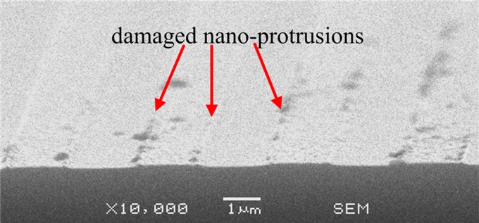
The damaged 2D silicon nano-mold, most of the nano-protrusions in the nano-mold has been damaged under embossing pressure of 2.5 MPa.
The effect of the embossing temperature on the replication precision was also analyzed. Fig. 5(b) shows the simulation results when the temperature was ranged from 65 °C to 105 °C under the optimized embossing pressure of 2 MPa. It can be seen that the replication precision of the 2D PET nanochannels increases significantly when the temperature increased from 65 °C to 75 °C. The replication precision of the 2D nanochannels was very low at the 65 °C. This could be caused by a reversible deformation related to the solid state of the PET material below the Tg of 71.3 °C.43 However, as the temperature increased to 75 °C, the PET was converted to a rubbery state and could be easily embossed with an irreversible deformation of the substrate, which results in great improvement of the replication precision. The replication precision of the 2D PET nanochannels was 99.6% under the temperature of 105 °C, while the replication precision of the 2D PET nanochannels was 99.2% under the temperature of 95 °C. Since the period of the fabrication is increased if the temperature is too high. To decrease the fabrication period, the temperature of 95 °C was chosen as the optimal temperature, although the replication precision at temperature of 95 °C is a little lower than at temperature of 105 °C. In addition, when the embossing time was longer than 100 s, the replication precision remained relatively unchanged and reached its maximum value of 99.2% under embossing temperature of 95 °C. For this reason, 100 s can be regarded as the optimal embossing time.
The pressure optimization (Fig. 5(a)) was performed under a not-optimized embossing temperature. Therefore, after optimizing the embossing temperature, the embossing pressure was re-optimized with optimized temperature of 95 °C (Fig. 5(c)). In Fig. 5(c), the embossing pressure of 2.5 MPa was not performed because the nano-mold was easily damaged under the embossing pressure of 2.5 MPa. From Fig. 5(c), when the embossing time is large than 100 s, the replication precision of the 2D PET nanochannels is 81.4%, 87.2%, 94.9%, and 99.2% at pressure of 0.5 MPa, 1 MPa, 1.5 MPa, and 2 MPa, respectively. The maximum replication precision of the 2D PET nanochannels can be obtained at pressure of 2 MPa. Therefore, we considered the embossing pressure of 2 MPa as the optimized embossing pressure.
The reason why the equilibrium values are varied with pressure and temperature can be explained as follows:
The deformation of the polymer can be expressed as44–46
| (4) |
where JT(t) is the creep compliance of the polymer at temperature T. JT(t) is a monotonic increasing function of time t. σ is the pressure applied on the polymer.
According to Eq. (4), when the embossing temperature is 75 °C and the embossing time is 200 s, the bigger the pressure applied on the polymer is, the larger the deformation of the polymer is. That means at high embossing pressure, the mold can be filled by the PET well. Therefore, in Fig. 5(a), the replication precision at pressure of 2.5 MPa is larger than that at pressure of 0.5 MPa, 1 MPa, 1.5 MPa, and 2 MPa. And in Fig. 5(c), the replication precision at pressure of 2 MPa is larger than that at pressure of 0.5 MPa, 1 MPa, and 1.5 MPa.
As reported by Mark,47 the higher temperature is associated with higher creep compliance JT(t) of the PET. According to Eq. (4), when the embossing pressure is 2 MPa and the embossing time is 100 s, higher embossing temperature correlates to larger deformation of the PET substrate. Therefore, in Fig. 5(b), the replication precision at temperature of 105 °C is larger than that at temperature of 65 °C, 75 °C, 85 °C, and 95 °C.
The optimized embossing parameters are temperature of 95 °C, pressure of 2 MPa, and time of 100 s. However, author reported that the PET embossing parameters can be temperature of 85 °C and pressure of 1.5 MPa during micro hot embossing.48 The viscoelastic polymer flows less easily into the cavity of the nano-mold than into the cavity of the micro-mold due to the effect of friction and surface tension.42 Higher pressure and temperature are required for the polymer to flow into the cavity of the nano-mold.
In order to verify the simulation method, a comparison between experiment and simulation results was performed. The PET substrates were embossed under different temperatures (65–95 °C) while using the optimized pressure of 2 MPa and time of 100 s. To calculate the standard deviations of the replication precision, we measure three samples for each embossing temperature (65 °C, 75 °C, 85 °C, or 95 °C). Because the distribution of the nanochannels in the sample is uniform, for each sample we measure one time. Figs. 7(a)–7(d) show the experiment and simulation profiles. In Figs. 7(a)–7(d), the images with 1 μm scale bars are the SEM pictures of the embossed PET nanochannels which are embossed at different temperature of 65 °C, 75 °C, 85 °C, and 95 °C, while the inserted images are the embossed PET nanochannels simulated at the corresponding temperatures. In comparison of the replication accuracy between the simulation and experimental results (Fig. 7(e)), the simulation results are in good agreement with experimental results. It is promising that the proposed simulation method can be used to analyze and optimize the hot embossing process.
FIG. 7.

Comparison of experiment and simulation results. (a)–(d) Comparison of experiment and simulation for 2D nanochannel profiles at the temperature of 65 °C, 75 °C, 85 °C, and 95 °C, respectively. The SEM images show the experiment results, while the inserted views show the simulation results. (e) Comparison of the replication precision between experiment and simulation results.
B. Influence of O2 plasma parameters on the PET substrate water contact angle
The surface properties of the PET substrate have a great impact on the bonding strength of the micro- and nanochannels. The higher degree of the hydrophilicity of PET substrate is associated with higher bonding strength. The hydrophilicity of the polymer can be evaluated by the water contact angle of the polymer. The lower water contact angle of the polymer correlates to the higher hydrophilicity of the polymer. O2 plasma treatment was conducted in a plasma etcher/asher (K1050X, Quorum/Emitech, UK). The effect of power and time on the water contact angle was analyzed to optimize the processing parameters of the O2 plasma treatment.
Fig. 8(a) shows the contact angle of the PET as a function of chamber power at an etching time of 15 s and an oxygen pressure of 60 Pa. The contact angle of native PET is 71.91°. After treated by O2 plasma, the contact angles of PET substrate were decreased. According to Fig. 8(a), the contact angle decreases sharply at the beginning (power lower than 15 W), and then remains relatively unchanged with increased power. Therefore, it can be assumed that the optimal chamber power for PET substrate is 15 W. Based on the optimal chamber power, the time influence of O2 plasma treatment on the contact angle was studied. Fig. 8(b) shows the contact angle of the PET as a function of time with an oxygen pressure of 60 Pa and the optimized chamber power of 15 W. The contact angle drops rapidly at the beginning of the treatment, and remains almost constant when the treatment time is longer than 35 s. Thus, the recommended optimal time for the O2 plasma treatment of PET substrate is 35 s.
FIG. 8.

The influence of O2 plasma treatment power (a) and time (b) on the contact angles of the PET substrate.
C. Optimization of the bonding parameters
Compared with the ultra-thin film spin-coated on the hard substrate used in thermal nanoimprint, the 1 mm thick PET sheet without the support of the hard substrate would bend more easily after the demolding process due to induced residual stress.23 The channels cannot be fully sealed during thermal bonding process due to the bended PET sheet after demolding, which would cause leakage problems.49 High bonding temperature and pressure can reduce the residual stress, but it caused the high distortion in the nanochannels resulting in blocking problem. The bonding rate of the chip (the ratio of the bonding area over the whole area of the chip) is introduced for evaluating the bonding quality of the channels.49 To fabricate a 2D PET nanofluidic chip with a bonding rate of 100%, the bonding temperature, pressure, and time should be optimized carefully.
The bonding rate of the chip was measured by using AutoCAD 2008 (Autodesk, San Rafael, California, USA). First, we scanned the bonded chip by a scanner (Canscan Lide 25, Canon, Japan) to obtain a JPG image of the bonded chip. Then the scanned image of the bonded chip was imported into AutoCAD. The bonding area and the entire area of the chip can be calculated by using the area measurement function in AutoCAD 2008. Fig. 9(a) shows the bonding rate of the nanofluidic chip as a function of the bonding time with different bonding pressures when the bonding temperature was 60 °C. When the bonding pressure was 0.05 MPa, the bonding rate of the PET nanofluidic chip was extremely low. This is because the patterned PET substrate cannot be in full contact with the PET cover plate at such a low bonding pressure. However, when the bonding pressure increased, the bonding rate of the nanofluidic chip improved remarkably. The bonding pressure of 0.2 MPa is recommended.
FIG. 9.

Experiment results of the thermal bonding process: (a) bonding pressure optimization, (b) bonding temperature optimization, and (c) bonding pressure re-optimization according the bonding rate of the 2D PET nanofluidic chip.
Fig. 9(b) shows the bonding rate as a function of the bonding time with different bonding temperatures when using the recommended bonding pressure of 0.2 MPa. The highest bonding temperature in Fig. 9(b) was 69 °C, because the nanochannels in the PET substrate would be highly distorted if the bonding temperature was above Tg of the PET substrate (71.3 °C). One can clearly see that the bonding rate increases with increasing bonding temperature. The bonding rate of the 2D nanofluidic chip improved greatly when the bonding temperature was 69 °C. The bonding rate of the 2D nanofluidic chip can reach 100% when the bonding time is longer than 20 min (at bonding temperature of 69 °C). In order to fully seal the nanofluidic chip, the bonding temperature we chose was 69 °C.
Since the bonding pressure optimization (Fig. 9(a)) was performed under a not-optimized bonding temperature, after optimizing the bonding temperature, the bonding pressure was re-optimized under optimized bonding temperature of 69 °C (Fig. 9(c)). In Fig. 9(c), the maximum bonding rate of 100% can only be obtained at bonding pressure of 0.2 MPa. When the bonding pressure was lower than 0.15 MPa, the bonding rate was below 95% and the bubbles (un-bonded area) can occur in the centre of the chip (the patterned area). Therefore, we considered the embossing pressure of 0.2 MPa as the optimized bonding pressure.
In order to determine the optimal bonding time, the fluorescence detections were performed to estimate the bonding quality of the micro- and nanochannels. In the dyed water test, de-ionized water containing a fluorescent dye (20 mg/ml solution of Rhodamine B in a 50% mixture of ethanol and de-ionized water) was filled into the bonded micro- and nanochannels by capillary force. The Rhodamine B molecules were excited by a mercury lamp of an inverted fluorescence microscope (Olympus IX71, Tokyo, Japan). Fig. 10 shows the fluorescence images of micro- and nanochannels filled with the liquid solution. The micro- and nanochannels in Figs. 10(a)–10(c) were bonded for different bonding time under the optimized bonding temperature and pressure, 69 °C and 0.2 MPa. In Fig. 10(a), when the bonding time was 20 min, a serious leakage problem occurred between the bonding interfaces. It indicates that the nanochannels were not fully bonded. However, when the bonding time was increased to 30 min, the micro- and nanochannels, as shown in Fig. 10(b), could be bonded together without any blocking or leakage throughout the entire length of the micro- and nanochannels. As shown in Fig. 10(c), when the bonding time was increased to 40 min, the brightness of the fluorescence image was lower than that of Fig. 10(b), which indicates that the Rhodamine B solution could not fill the nanochannels easily. This may be due to a distortion of the nanochannels even though there was no leakage or complete blocking. For this reason, 30 min was chose as the optimal bonding time.
FIG. 10.

Fluorescence images of the nanochannels filled with a fluorescent dye solution for the nanofluidic chips bonded at different times of (a) 20 min, (b) 30 min, and (c) 40 min.
Finally, the bonding parameters are optimized for pressure of 0.2 MPa, temperature of 69 °C, and time of 30 min to fully bonding the PET nanochannels.
D. A method to measure the deformation of the bonded nanochannels
In order to measure any possible deformation, the cross-sectional profile of nanochannels after the thermal bonding process must be observed. It is difficult to prepare a cross-sectional profile of the bonded nanochannels when the polymer substrate is excessively thick. To make the nanochannels accessible for observation, the cover plate and the nano-patterned substrate must be carefully separated by hand. Then, the deformation of the nano-patterned substrate and the cover plate can be measured individually and the deformation of the bonded nanochannels can be determined.33,34 However, for the nanochannels bonded by O2 plasma assisted thermal bonding method, the nanochannels will be highly distorted after separating the cover plate and patterned substrate due to the high bonding strength.
We found that the bonding strength can be intentionally decreased by omitting the O2 plasma treatment. The bonded nanochannles without the O2 plasma treatment can be easily separated without any damage. To estimate the deformation of the bonded nanochannels, it is a good practice to bond the nanochannels without O2 plasma treatment, followed by separating the PET cover plate and the patterned PET substrate to make the channels accessible to observe (we call this interchange method). However, during the thermal bonding process, the O2 plasma might influence the deformation of nanochannels. Therefore, the influence of the O2 plasma on the deformation of the 2D PET nanochannels should be investigated.
During the thermal bonding process, the bonding temperature is always below Tg, thus the polymer can be assumed to be an elastic material.39,50 For an elastic polymer material, the deformation of the elastic polymer can be expressed as
| (5) |
where σ is the bonding pressure and E is the Young modulus of the polymer.
It can be seen that if the bonding pressure is a constant value, the deformation of the 2D polymer nanochannels will be only influenced by Young modulus of the polymer. The O2 plasma will not influence the deformation of the 2D PET nanochannels if it cannot affect the Young modulus of the polymer. The deformation of the bonded 2D PET nanochannels can be estimated by the interchange method.
The Young moduli of the PET substrate before and after the O2 plasma treatment was measured by the Nano Indenter XP system (America, 100BA-1C). The Young modulus in Fig. 11 is the average value of six individual measurements. The modified PET substrate was O2 plasma treated by using the optimized parameters (chamber power of 15 W, time of 35 s and pressure of 60 Pa). From Fig. 11, we can clearly see that the Young modulus of the PET substrate is not altered after the plasma treatment. According to the discussion above, the deformation of the 2D polymer nanochannels will thus not be affected. Therefore, it is feasible to estimate the deformation of the bonded 2D PET nanochannles by the interchange method.
FIG. 11.

The comparison of Young modulus of native PET substrates and the PET substrate treated by the O2 plasma with chamber power of 15 W, time of 35 s, and a pressure of 60 Pa.
E. The deformation of bonded micro- and nanochannels
1. The deformation of bonded nanochannels
The deformation of bonded 2D PET nanochannels was assessed. Fig. 12 shows the deformation of the patterned 2D PET nanochannels before and after the thermal bonding process. Fig. 13 shows the deformation of the PET cover plate after the thermal bonding process.
FIG. 12.

The SEM images show the profile of 2D PET nanochannels. The measured profiles are (a) 174.67 ± 4.51 nm wide and 179.00 ± 4.00 nm deep nanochannels before thermal bonding and (b) 170.33 ± 2.52 nm wide and 172.00 ± 3.00 nm deep nanochannels after thermal bonding with bonding temperature of 69 °C, pressure of 0.2 MPa, and time of 30 min observed by the interchange method.
FIG. 13.

The surface topography of the PET cover plate, the maximum height of the nano-protrusions in the cover plate is 11.33 ± 2.52 nm. The PET cover plate was boned with PET substrate (with nanochannels) under bonding temperature of 69 °C, pressure of 0.2 MPa, and time of 30 min.
To calculate the standard deviation of the width and depth of the nanochannels, we measured three samples. In Fig. 12, the nanochannels were 174.67 ± 4.51 nm wide and 179.00 ± 4.00 nm deep before the thermal bonding and 170.33 ± 2.52 nm wide and 172.00 ± 3.00 nm deep after the thermal bonding process observed by interchange method.
The PET cover plate was boned with PET substrate (with nanochannels) under bonding temperature of 69 °C, pressure of 0.2 MPa, and time of 30 min. The deformation of PET cover plate was measured by a stylus profilometer (ET4000 M, Kosaka, Japan). The maximum height of the nano-protrusions of the cover plate is 11.33 ± 2.52 nm, which indicates that the PET cover plate has sunk into the 2D nanochannels (Fig. 13). It has been suggested that such deformation can be tolerated.20 The estimated total dimension loss of the bonded 2D PET nanochannels was 4.34 ± 7.03 nm and 18.33 ± 9.52 nm in width and depth, respectively.
2. The deformation of bonded microchannels
To calculate the standard deviation of the width and depth of the microchannels, we measured three samples. The microchannels cross-sections of before and after the thermal bonding process are shown in Fig. 14. The profiles were observed by an optical microscope (Olympus STM6, Japan). The microchannels were 117.67 ± 2.08 μm wide and 16.47 ± 1.30 μm deep before the thermal bonding process and 115.83 ± 0.67 μm wide and 16.00 ± 0.20 μm deep after the thermal bonding process.
FIG. 14.

The microscope images of the PET microchannels: (a) 117.67 ± 2.08 μm wide and 16.47 ± 1.30 μm deep microchannels before thermal bonding and (b) 115.83 ± 0.67 μm wide and 16.00 ± 0.20 μm deep microchannels after thermal bonding with a bonding temperature of 69 °C, pressure of 0.2 MPa and time of 30 min observed by the interchange method.
The deformation of PET cover plate was measured by a stylus profilometer. The maximum height of the micro-protrusions of the PET cover plate is 0.49 ± 0.04 μm (Fig. 15), which shows that the PET cover plate sank into the PET substrate. The total dimension loss of bonded microchannels was 1.84 ± 2.75 μm in width and 0.96 ± 1.54 μm in depth, respectively. Compared with their sizes, the deformation of bonded PET microchannels is extremely small.
FIG. 15.
The surface topography of the PET cover substrate, the maximum height of the micro-protrusion in the cover plate is 0.49 ± 0.04 μm.
The bonding strength is defined as the ratio of the tensile force that separated the cover plate from substrate over the area of the chip. The bonding strength of 2D PET nanofluidic chip measured by a tensile tester (CSS Universal Material Testing Machine, Changchun Research Institute for Testing Machine Co., Ltd, China) was 0.664 MPa. Fig. 16 shows photograph of the 2D PET nanofluidic chip fabricated by hot embossing and O2 plasma assisted thermal bonding techniques. The fluorescence detection has been performed to estimate the bonding quality of the micro- and nanochannels. The enlarged view in Fig. 16 shows the fluorescence images captured by fluorescence microscope that prove the absence of blocking and leakage over the entire length of micro- and nanochannels.
FIG. 16.

Photograph of the 2D PET nanofluidic chip using the hot embossing technique. The enlarged view shows the fluorescence image of the nanochannels.
IV. CONCLUSIONS
A 2D PET nanofluidic chip was fabricated by hot embossing and thermal bonding techniques in the present work. To evaluate the replication precision of the 2D PET nanochannels, the influence of the hot embossing parameters was investigated by both finite element method and experiments. With optimized parameters (temperature of 95 °C, pressure of 2 MPa, and time of 100 s) 2D PET nanochannels were replicated into the PET substrate with high replication precision of 98.4%. The fabricated PET nanochannels were bonded with a PET cover plate by O2 plasma assisted thermal bonding method. To increase the bonding strength of the nanofluidic chip and decrease the dimension loss of bonded micro- and nanochannels, the parameters of the bonding process were optimized according the bonding rate of nanofluidic chip. With the optimized parameters (O2 plasma treatment: chamber power of 15 W, time of 35 s, and pressure of 60 Pa; thermal bonding process: bonding temperature of 69 °C, pressure of 0.2 MPa, and time of 30 min), the 2D PET nanofluidic chip was successfully fabricated with a high bonding strength of 0.664 MPa. According to the experiment results, the total dimension loss of bonded 2D nanochannels was 4.34 ± 7.03 nm and 18.33 ± 9.52 nm in width and depth, respectively, while the total dimension loss of the bonded microchannels was 1.84 ± 2.75 μm and 0.96 ± 1.54 μm in width and depth, respectively. Finally, the fabricated 2D nanofluidic chip was characterized using a Rhodamine B solution, which demonstrated a successful bonding between substrate and covering layer without blocking or leakage over the entire length of the micro- and nanochannels. It is expected that the presented fabrication technology can provide means for low-cost and high-throughput 2D plastic nanofluidic chips fabrication.
ACKNOWLEDGMENTS
This project was supported by National Natural Science Foundation of China (Grant Nos. 91023046 and 51075059) and Specialized Research Fund for the Doctoral Program of Higher Education of China (SRFDP) (Grant No. 20120041110034).
References
- 1.Sparreboom W., Berg A. van den, and Eijkel J. C. T., Nat. Nanotechnol. 4, 713 (2009). 10.1038/nnano.2009.332 [DOI] [PubMed] [Google Scholar]
- 2.Abgrall P. and Nguyen N. T., Anal. Chem. 80, 2326 (2008). 10.1021/ac702296u [DOI] [PubMed] [Google Scholar]
- 3.Freedman K. J., Haq S. R., Edel J. B., Jemth P., and Kim M. J., Sci. Rep. 3, 1638 (2013). 10.1038/srep01638 [DOI] [PMC free article] [PubMed] [Google Scholar]
- 4.Eijkel J. C. T. and Berg A. van den, Microfluid. Nanofluid. 1, 249 (2005). 10.1007/s10404-004-0012-9 [DOI] [Google Scholar]
- 5.Anwar K., Han T., and Kim S. M., in Fluid Measurements and Instrumentation Cavitation and Multiphase Flow Advances in Fluids Engineering Education Microfluidics (2012), Vol. 2, p. 409. [Google Scholar]
- 6.Chun D. W., Kim S. H., Song H., Kwak S., Kim Y. C., Seok H. G., Lee S. M., and Lee J. H., Appl. Phys. Express 6, 017001 (2013). 10.7567/APEX.6.017001 [DOI] [Google Scholar]
- 7.Sang J., Du H., Wang W., Chu M., Wang Y., Li H., Zhang H. A., Wu W., and Li Z., Biomicrofluidics 7, 024112 (2013). 10.1063/1.4802936 [DOI] [PMC free article] [PubMed] [Google Scholar]
- 8.van Kan J. A., Zhang C., Malar P. P., and van der Maarel J. R. C., Biomicrofluidics 6, 036502 (2012). 10.1063/1.4740231 [DOI] [PMC free article] [PubMed] [Google Scholar]
- 9.Pedersen J. N., Marie R., Bauer D. L. V., Rasmussen K. H., Yusuf M., Volpi E. V., Kristensen A., Mir K. U., and Flyvbjerg H., Biophys. J. 104, 175A (2013). 10.1016/j.bpj.2012.11.986 [DOI] [PMC free article] [PubMed] [Google Scholar]
- 10.Zhou K. M., Li L. C., Tan Z. N., Zlotnick A., and Jacobson S. C., J. Am. Chem. Soc. 133, 1618 (2011). 10.1021/ja108228x [DOI] [PMC free article] [PubMed] [Google Scholar]
- 11.Tsukahara T., “Nanofluidic-based separation system of radionuclide ions by controlling electrostatic forces,” Bull. Res. Lab. Nucl. Reactors 34, 51 (2010). [Google Scholar]
- 12.Gillespie D. and Pennathur S., Anal. Chem. 85, 2991 (2013). 10.1021/ac400081p [DOI] [PubMed] [Google Scholar]
- 13.Tsukahara T., Mawatari K., and Kitamori T., Chem. Soc. Rev. 39, 1000 (2010). 10.1039/b822557p [DOI] [PubMed] [Google Scholar]
- 14.Abad E., Juarros A., Retolaza A., Merino S., Marie R., and Kristensen A., Microelectron. Eng. 88, 300 (2010). 10.1016/j.mee.2010.11.025 [DOI] [Google Scholar]
- 15.Xu Y., Wang C. X., Li L. X., Matsumoto N., Jang K., Dong Y. Y., Mawatari K., Suga T., and Kitamori T., Lab Chip 13, 1048 (2013). 10.1039/c3lc41345d [DOI] [PubMed] [Google Scholar]
- 16.Harms Z. D., Mogensen K. B., Nunes P. S., Zhou K. M., Hildenbrand B. W., Mitra I., Tan Z. N., Zlotnick A., Kutter J. P., and Jacobson S. C., Anal. Chem. 83, 9573 (2011). 10.1021/ac202358t [DOI] [PMC free article] [PubMed] [Google Scholar]
- 17.Menard L. D. and Ramsey J. M., Nano Lett. 11, 512 (2011). 10.1021/nl103369g [DOI] [PMC free article] [PubMed] [Google Scholar]
- 18.Menard L. D. and Ramsey J. M., Anal. Chem. 85, 1146 (2013). 10.1021/ac303074f [DOI] [PMC free article] [PubMed] [Google Scholar]
- 19.Liu F., Tan K. B., Malar P., Bikkarolla S. K., and van Kan J. A., Microelectron. Eng. 102, 36 (2012). 10.1016/j.mee.2012.05.020 [DOI] [Google Scholar]
- 20.Hsu Y. C. and Chen T. Y., Biomed. Microdevices 9, 513 (2007). 10.1007/s10544-007-9059-1 [DOI] [PubMed] [Google Scholar]
- 21.Vlachopoulou M. E., Tserepi A., Pavli P., Argitis P., Sanopoulou M., and Misiakos K., J. Micromech. Microeng. 19, 015007 (2009). 10.1088/0960-1317/19/1/015007 [DOI] [Google Scholar]
- 22.Tran H. H., Wu W., and Lee N. Y., Sens. Actuators B 181, 955 (2012). 10.1016/j.snb.2012.11.060 [DOI] [Google Scholar]
- 23.Liang Y., Liu C., Sun H., Li J., Liu J., and Gao X., Adv. Mater. Res. 60–61, 450 (2009). 10.4028/www.scientific.net/AMR.60-61.450 [DOI] [Google Scholar]
- 24.Wu J. H., Chantiwas R., Amirsadeghi A., Soper S. A., and Park S., Lab Chip 11, 2984 (2011). 10.1039/c1lc20294d [DOI] [PubMed] [Google Scholar]
- 25.Wu Y. L., Lin J. J., Hsu P. Y., and Hsu C. P., Sens. Actuators B 155, 709 (2011). 10.1016/j.snb.2011.01.035 [DOI] [Google Scholar]
- 26.Sunkara V., Park D. K., and Cho Y. K., RSC Adv. 2, 9066 (2012). 10.1039/c2ra20880f [DOI] [Google Scholar]
- 27.Sun Y., Kwok Y. C., and Nguyen N. T., J. Micromech. Microeng. 16, 1681 (2006). 10.1088/0960-1317/16/8/033 [DOI] [Google Scholar]
- 28.Zhu X., Liu G., Guo Y., and Tian Y., Microsystem Technol. 13, 403 (2007). 10.1007/s00542-006-0224-x [DOI] [Google Scholar]
- 29.Zhang Z. B., Wang X. D., Luo Y., He S. Q., and Wang L. D., Talanta 81, 1331 (2010). 10.1016/j.talanta.2010.02.031 [DOI] [PubMed] [Google Scholar]
- 30.Ng S. H., Tjeung R. T., Wang Z. F., Lu A. C. W., Rodriguez I., and Rooij N. F. de, Microsyst. Technol. 14, 753 (2008). 10.1007/s00542-007-0459-1 [DOI] [Google Scholar]
- 31.Tsao C. W. and DeVoe D. L., Microfluid. Nanofluid. 6, 1 (2009). 10.1007/s10404-008-0361-x [DOI] [Google Scholar]
- 32.Yussuf A. A., Sbarski I., Hayes J. P., Solomon M., and Tran N., J. Micromech. Microeng. 15, 1692 (2005). 10.1088/0960-1317/15/9/011 [DOI] [Google Scholar]
- 33.Jena R. K., Chester S. A., Srivastava V., Yue C. Y., Anand L., and Lam Y. C., Sens. Actuator B 155, 93 (2011). 10.1016/j.snb.2010.11.031 [DOI] [Google Scholar]
- 34.Chantiwas R., Hupert M. L., Pullagurla S. R., Balamurugan S., Tamarit-Lopez J., Park S., Datta P., Goettert J., Cho Y. K., and Soper S. A., Lab Chip 10, 3255 (2010). 10.1039/c0lc00096e [DOI] [PubMed] [Google Scholar]
- 35.Rao J., Zou H. L., Syms R. R. A., Cheng E., and Liu C., Micro Nano Lett. 6, 29 (2011). 10.1049/mnl.2010.0155 [DOI] [Google Scholar]
- 36.Cheng E., Zou H. L., Yin Z. F., Jurčíček P., and Zhang X., J. Micromech. Microeng. 23, 075022 (2013). 10.1088/0960-1317/23/7/075022 [DOI] [Google Scholar]
- 37.Chantiwas R., Park S., Soper S. A., Kim B. C., Takayama S., Sunkara V., Hwang H., and Cho Y. K., Chem. Soc. Rev. 40, 3677 (2011). 10.1039/c0cs00138d [DOI] [PMC free article] [PubMed] [Google Scholar]
- 38.Takagi H., Takahashi M., Maeda R., Onishi Y., Iriye Y., Iwasaki T., and Hirai Y., Microelectron. Eng. 85, 902 (2008). 10.1016/j.mee.2008.01.018 [DOI] [Google Scholar]
- 39.Lan S., Lee H. J., Lee S. H., Ni J., Lai X., Lee H. W., Song J. H., and Lee M. G., Mater. Des. 30, 3879 (2009). 10.1016/j.matdes.2009.03.045 [DOI] [Google Scholar]
- 40.Cheng E., Yin Z. F., Zou H. L., and Jurčíček P., J. Micromech. Microeng. 24, 015004 (2014). 10.1088/0960-1317/24/1/015004 [DOI] [Google Scholar]
- 41.Williams M. L., Landel R. F., and Ferry J. D., J. Am. Chem. Soc. 77, 3701 (1955). 10.1021/ja01619a008 [DOI] [Google Scholar]
- 42.Yin Z. F., Cheng E., Zou H. L., and Jurčíček P., Polym. Eng. Sci. 54, 2398–2406 (2013). 10.1002/pen.23790 [DOI] [Google Scholar]
- 43.Guo L. J., J. Phys. D: Appl. Phys. 37, R123 (2004). 10.1088/0022-3727/37/11/R01 [DOI] [Google Scholar]
- 44.Zhang Y., Theory of Themo-Viscoelasticity ( Tianjin University Press, China, 2002), pp. 16–21. [Google Scholar]
- 45.Progelhof R. C., Throne J. L., and Progelhof R., Polymer Engineering Principles: Properties, Processes, and Tests for Design ( Hanser, American, 1993), pp. 250–260. [Google Scholar]
- 46.Aklonis J. J. and MacKnight W. J., Introduction to Polymer Viscoelasticity ( Wiley, American, 1983), pp. 45–65. [Google Scholar]
- 47.Mark J. E., Physical Properties of Polymers Handbook ( Springer, Germany, 2006), pp. 435–436. [Google Scholar]
- 48.Li J. M., Liu C., Qiao H. C., Zhu L. Y., Chen G., and Dai X. D., J. Micromech. Microeng. 18, 015008 (2008). 10.1088/0960-1317/18/1/015008 [DOI] [Google Scholar]
- 49.Du L., Chang H., Song M., and Liu C., Microsyst. Technol. 18, 423 (2012). 10.1007/s00542-012-1466-4 [DOI] [Google Scholar]
- 50.Kim N. W., Kim K. W., and Sin H. C., Microelectron. Eng. 8, 1858 (2008). 10.1016/j.mee.2008.05.030 [DOI] [Google Scholar]