

Abstract
Photovoltaic efficiency in solar cells is hindered by many unwanted effects. Radiative channels (emission of photons) sometimes mediated by nonradiative ones (emission of phonons) are principally responsible for the decrease in exciton population before charge separation can take place. One such mechanism is electron–hole recombination at surfaces or defects where the in-gap edge states serve as the nonradiative channels. In topological insulators (TIs), which are rarely explored from an optoelectronics standpoint, we show that their characteristic surface states constitute a nonradiative decay channel that can be exploited to generate a protected photovoltaic current. Focusing on two-dimensional TIs, and specifically for illustration purposes on a Bi(111) monolayer, we obtain the transition rates from the bulk excitons to the edge states. By breaking the appropriate symmetries of the system, one can induce an edge charge accumulation and edge currents under illumination, demonstrating the potential of TI nanoribbons for photovoltaics.
Keywords: Photovoltaics, Topological insulator, Exciton, Optics, Two-dimensional materials
The creation of pairs of a free electron and a hole may suffice to broadly explain the optical conductivity of insulators and semiconductors, but in general, bound electron–hole (e–h) pairs or excitons also play a non-negligible role.1−3 This is particularly true in two-dimensional (2D) crystals, where excitons become tightly bound due to the strong confinement and low screening. These include, for instance, hexagonal boron nitride4,5 or transition-metal dichalcogenides, which have been extensively studied in this regard.6−8 Additionally, it has also been shown that nonlinear phenomena such as high-harmonic generation9 and bulk photovoltaic effects10,11 can be greatly enhanced in 2D crystals.12−15 This, together with the high tunability of the atomic structure through strain16 and the ability to select excitations based on the light polarization, renders 2D optoelectronics as a very active field from both fundamental and technological perspectives.17 Of particular interest is light–energy conversion in the form of photocurrent generation, on which solar cell devices are based. The formation of bound e–h pairs and their subsequent separation is the most common source of photocurrent generation. In conventional solar cells, based on p–n junctions, this is achieved with the built-in electric field in the depletion zone, which separates the free charge carriers generating a chemical potential difference or a current depending on the circuit scheme. Since the efficiency of conventional cells is constrained by the Shockley–Queisser limit,18 alternative dissociation mechanisms have been proposed as in multijunction cells19 or in excitonic solar cells, where a bound electron–hole pair is formed and diffuses to an interface where the charge separation takes place.20,21
Topological insulators (TIs), on the other hand, have garnered significant attention in recent years due to their potential for use in spintronic devices, among other more fundamental reasons.22 However, there has been relatively little study of TIs from an optical perspective.23−32 Only recently, for instance, the exciton spectrum in Bi2Se3 was shown to exhibit topological properties.33
While there are works addressing the role of trivial edge states in the dissociation of excitons in semiconductors,34−38 the interaction between bulk excitons in TIs and their topologically protected edge states remains largely unexplored. One recent work studies the interplay between bulk and topological states in the formation of excitons in Bi2Se3 and how these affect the optical response of the TI.39
According to Fermi’s golden rule, an exciton is expected to decay elastically into a continuum of states in the presence of a given coupling. Excitons lie within the energy gap, and in a trivial insulator, there are typically no pure electronic excitations accessible for the exciton to decay into. In general, the usual dissociation channels would be radiative (photons) or nonradiative (phonons) recombination.40,41 Topological insulators, instead, always present edge states connecting the valence and conduction bands,42 meaning that in addition to light emission, the exciton can decay into e–h pairs formed by edge states. Our principal observation here is that, for sufficiently narrow 2D TI systems (TI ribbons), the electron and hole can also decay onto opposite edges, resulting in a charge separation and eventually in a photovoltaic current.
A purely electronic exciton decay can take place in the form of a noninteracting e–h pair where both constituents are located on the same edge or on opposite edges, which may result in charge transportation since edge electrons and holes typically have finite velocity. Due to time-reversal invariance, however, there is a k ↔ −k symmetry in the electronic bands (see Figure 2b), meaning that the e–h pair can be equally located at either k or −k, preventing such a possibility for both inter- and intraedge processes. On top of time-reversal invariance, note also that the system may possess inversion symmetry, forcing any current appearing on one edge to be canceled by the one appearing on the opposite one.
Figure 2.
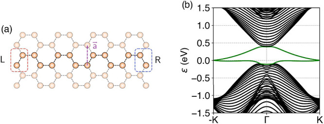
(a) Bi(111) zigzag nanoribbon where the dissociation process takes place. The highlighted atoms denote the unit cell, and a⃗ is the Bravais vector. The edge atoms are identified with the rectangles and labeled as L (left) or R (right). We introduce onsite energies on the left edge to split the topological edge bands. (b) Band structure of a Bi(111) zigzag ribbon for N = 20, with the edge bands highlighted in green.
Even if a priori one is unable to generate current in the presence of time-reversal symmetry, it is still possible to generate a charge imbalance between the edges. Consider that we introduce an asymmetry between the edges via an electric field applied in the direction perpendicular to the infinite edges or simply by some asymmetric termination. The latter is implemented in the following Hamiltonian
| 1 |
where the first three terms correspond to H0, which is a Slater–Koster tight-binding model of a ribbon of Bi(111),44 known to be a topological insulator.45−48 The last term is the edge offset potential. In particular, we work with a zigzag termination.46,49 The width of the ribbon is given by N, which is the number of dimers in the ribbon, taken to be even. In Figure 2(a), we show an example unit cell of the Bi(111) ribbon, and we identify the atoms as left (L) and right (R). On the left ones, we introduce additional onsite energies corresponding to the edge offset to split the edge bands. Then, as long as the perturbation does not close the bulk gap, the edge bands will split, as schematically shown in Figure 3(b). The splitting is expected to produce a different transition rate depending on whether the e–h pair is localized on the left–right boundaries, respectively, or the right–left ones.
Figure 3.
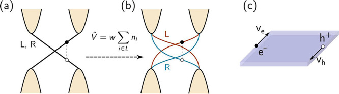
Splitting of the edge bands. (a) For a topological insulator with inversion symmetry, the edge bands of both sides are degenerate, resulting in identical rates for intraedge and interedge transitions. (b) The introduction of an edge offset potential allows the splitting of the edge bands, producing a distinction among the different transitions. (c) For each edge e–h pair, we can determine its total velocity as ve–h = ve – vh(43) to establish whether it carries current. For the pair drawn in (b), we observe that ve > 0 and vh < 0, meaning that ve–h = ve – vh > 0. (See the Supporting Information for the definition of the velocity.)
In addition to charge accumulation, current generation is also possible if time-reversal symmetry is broken. This may occur by the selective population of excitons with nonzero Q, avoiding their time-reversal partners with opposite momentum. One possible way to achieve this is shown in Figure 1, where an exciton wave packet is created in the bulk of the sample. This packet is generically described by a momentum distribution |X⟩ = ∫ dQ f(Q)|X(Q)⟩. Since excitons with finite momentum also have finite velocity, some of them will propagate into the top ribbon where the edge offset is present. This populates the ribbon with excitons with finite Q but not their time-reversal companions. From the dissociation of these excitons into interedge electron–hole pairs, we expect to generate a topologically protected photocurrent.
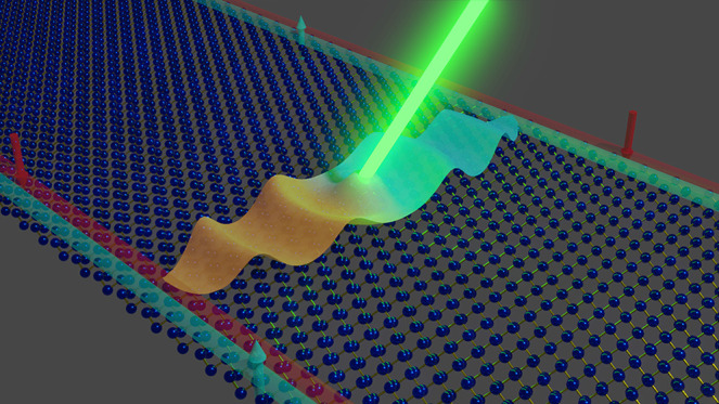
Figure 1.
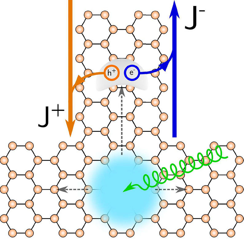
Schematic representation of the proposed mechanism. Device where an exciton wave packet is created at the bulk of the sample, where it will diffuse in any direction. Excitons entering the top ribbon present a finite momentum Q, giving rise to an out-of-equilibrium edge carrier population with nonzero momentum and velocity, thus forming a topologically protected current.
To test these hypothesis, we need to evaluate the transition rate from the exciton to each one of the possible electron–hole pairs. Instead of using the band number, we denote each band by its location or edge index, R (right) and L (left). Thus, for instance, an electron and a hole located on the opposite edges with momentum k would be |L, R, k⟩. With this notation, we want to evaluate the following transition rates
| 2 |
where s, s′ ∈ {R, L} denotes the edge where the electron, hole are localized, respectively, ρ is the density of states of the final continuum of states, namely, the edge e–h pairs, and V is the electrostatic interaction. EX is the energy of the exciton state, defined as the energy of the state relative to the Fermi sea. The initial exciton |X⟩ is taken as the bulk ground-state exciton
| 3 |
which is a superposition of electron–hole
pairs between any conduction (c) and valence (v) bands, excluding the edge bands. |FS⟩ denotes the Fermi sea, and the coefficients  which determine the exciton states are
obtained by solving the Bethe–Salpeter equation.50−53 Specifically, we assume that all orbitals are point-like, which
greatly simplifies the calculation of the exciton spectrum.54−57 Regarding screening, we use the Rytova–Keldysh potential.58−61 The edge e–h pair is defined as
which determine the exciton states are
obtained by solving the Bethe–Salpeter equation.50−53 Specifically, we assume that all orbitals are point-like, which
greatly simplifies the calculation of the exciton spectrum.54−57 Regarding screening, we use the Rytova–Keldysh potential.58−61 The edge e–h pair is defined as
| 4 |
where  creates a conduction electron such that
it is located at side s with the specified momentum.
The same is done with cs′k for the valence hole.
creates a conduction electron such that
it is located at side s with the specified momentum.
The same is done with cs′k for the valence hole.
k is chosen such that, given s, s′, the corresponding e–h pair has the same energy as the exciton. In the case of degeneracies, the rates are obtained by summing over all of the degenerate states. The sign of k must also be specified since there are two possibilities and, in principle, transitions can be asymmetric in ±k. When the inversion symmetry is removed by the edge offset potential w, e.g., at the left boundary, the edge bands, as shown in Figure 4(a), are split. We expect now that the interedge transition rates ΓRL and ΓLR will be different as the interedge e–h pairs correspond to different |k| points (see Figure 4(a)), producing an interedge charge imbalance in the material. This mechanism would compete with intraedge transitions ΓRR and ΓLL, where the electron and hole eventually recombine on the same edge. The intraedge rates serve then as the baseline to estimate the efficiency of the effect.
Figure 4.
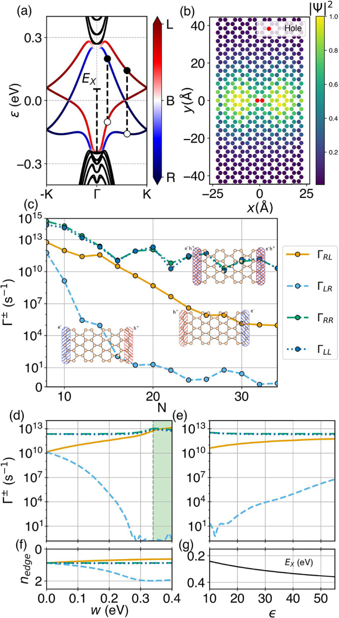
Transitions at Q = 0. (a) Band structure of the Bi(111) ribbon for N = 20 and w = 0.2 eV. The edge bands are colored according to the electronic occupation at the edges of the ribbon. (b) Real-space electronic density probability of the ground-state exciton for N = 12. (c) Transition rates of the ground-state exciton to the different edge electron–hole pairs as a function of the width of the ribbon N for w = 0.2 eV. (d, f) Transition rates and edge occupation as a function of the edge offset potential w for N = 14. (e, g) Transition rates and ground-state exciton energy as a function of the dielectric constant ε for N = 14. (c, d, e, and f) share the same legend.
Regarding the transition rates for Q = 0, because
of time-reversal symmetry, the transition rates are symmetric in +k ↔ −k (i.e.,  for Q = 0 excitons) (see
proof in the Supporting Information). The
rates in the presence of an onsite potential (w =
0.2 eV) as a function of the width of the ribbon N are shown in Figure 4c. In general, as expected, the interedge rates decay faster as a
function of N than the intraedge ones, with
for Q = 0 excitons) (see
proof in the Supporting Information). The
rates in the presence of an onsite potential (w =
0.2 eV) as a function of the width of the ribbon N are shown in Figure 4c. In general, as expected, the interedge rates decay faster as a
function of N than the intraedge ones, with  being several orders of magnitude higher
than
being several orders of magnitude higher
than  for N ≈ 10–30.
Notably, for intermediate widths (N ≈ 12–16),  turns out to be comparable to intraedge
rates. This can be attributed, in part, to the peculiar real-space
electronic probability density of the exciton, which exhibits p-like
character, as shown Figure 4(b). Moreover, it is possible to tune the rates to enhance
the interedge/intraedge ratio. In Figure 4(d), we show the effect of modifying the
edge onsite potential w. For w =
0, there is no charge imbalance since both interedge rates are equal.
As we increase the potential, one rate
turns out to be comparable to intraedge
rates. This can be attributed, in part, to the peculiar real-space
electronic probability density of the exciton, which exhibits p-like
character, as shown Figure 4(b). Moreover, it is possible to tune the rates to enhance
the interedge/intraedge ratio. In Figure 4(d), we show the effect of modifying the
edge onsite potential w. For w =
0, there is no charge imbalance since both interedge rates are equal.
As we increase the potential, one rate  becomes enhanced as it comes closer to
the intraedge rates, while the other
becomes enhanced as it comes closer to
the intraedge rates, while the other  decreases. The effect of the onsite potential
approximately splits the edge bands by the same value w. Therefore, as we increase w, the corresponding
edge pairs become increasingly more distant in |k|. In Figure 4(a),
we see that those involved in
decreases. The effect of the onsite potential
approximately splits the edge bands by the same value w. Therefore, as we increase w, the corresponding
edge pairs become increasingly more distant in |k|. In Figure 4(a),
we see that those involved in  get pushed to the high-symmetry point K, where the wave functions are fully localized on the edge.
On the other hand, for
get pushed to the high-symmetry point K, where the wave functions are fully localized on the edge.
On the other hand, for  , the e–h pairs involved get closer
to Γ (k = 0), where the functions have a stronger
bulk component. Therefore, it is possible to improve the interedge/intraedge
ratio by tuning the localization of the e–h pairs on the edge,
as seen in Figure 4(d). If the edge bands become too far apart, then some of the electron–hole
pairs start localizing at different bands, which we indicate with
the green region.
, the e–h pairs involved get closer
to Γ (k = 0), where the functions have a stronger
bulk component. Therefore, it is possible to improve the interedge/intraedge
ratio by tuning the localization of the e–h pairs on the edge,
as seen in Figure 4(d). If the edge bands become too far apart, then some of the electron–hole
pairs start localizing at different bands, which we indicate with
the green region.
A similar discussion can be carried out with the dielectric constants of the system. We focus on the dielectric constant of the material ϵ, although the same arguments apply to the substrate constant ϵs. Tuning ϵ produces a change in the exciton energy, which will result in a transition to pairs with different k, as shown in Figure 4(e,g). In this case, the specific behavior will be dependent on the form of the bands. Similar to the onsite potential, changing the exciton energy drastically could result in pairs hosted in a different set of bands from before, although this is not the case for the range of values considered.
With respect
to transition rates for Q ≠
0, next we consider the transition rates for excitons with finite
momentum Q. As for Q = 0 excitons,
the edge charge accumulation will still be present as long as we keep
the edge offset term finite (we again set a fixed value of w = 0.2 eV). Now, the main difference with respect to the
rates for Q = 0 excitons comes from the asymmetry
in k. Since the initial exciton is not time-reversal-invariant
(as it has finite momentum Q), all of the transition
rates  will be different. (Figure 5(a) shows the interedge processes schematically.)
Both intraedge and interedge pairs can carry a net current since they
have a finite total velocity ve–h(k) ≠ 0, but now there will be no exact cancellation
between k and −k pairs.
will be different. (Figure 5(a) shows the interedge processes schematically.)
Both intraedge and interedge pairs can carry a net current since they
have a finite total velocity ve–h(k) ≠ 0, but now there will be no exact cancellation
between k and −k pairs.
Figure 5.

Transitions
at finite Q. (a, b) Band structure
of the Bi(111) ribbon for N = 20 and w = 0.2 eV. The first one shows the edge occupation of the bands,
and the second one shows the average spin projection  of the bands. (c) Transition rates of the
ground-state exciton as a function of Q for N = 14. (d) Low-energy exciton band structure. Each color
corresponds to four excitonic states in total. (e) Center-of-mass
velocity of the ground-state exciton. The shadowed region denotes
the fraction of excitons that do not contribute to the formation of
an edge current. (f) Velocity v = ve – vh of the relevant
electron–hole pair
of the bands. (c) Transition rates of the
ground-state exciton as a function of Q for N = 14. (d) Low-energy exciton band structure. Each color
corresponds to four excitonic states in total. (e) Center-of-mass
velocity of the ground-state exciton. The shadowed region denotes
the fraction of excitons that do not contribute to the formation of
an edge current. (f) Velocity v = ve – vh of the relevant
electron–hole pair  and of each component individually, for N = 14 and w = 0.2 eV. (g) Transition rates
as a function of N for Q = 0.1 Å–1 and w = 0.2 eV. (h) Transition rates
as a function of the staggered potential Vst for N = 14 and w = 0.2 eV. The inset shows the total spin projection of the ground-state
exciton,
and of each component individually, for N = 14 and w = 0.2 eV. (g) Transition rates
as a function of N for Q = 0.1 Å–1 and w = 0.2 eV. (h) Transition rates
as a function of the staggered potential Vst for N = 14 and w = 0.2 eV. The inset shows the total spin projection of the ground-state
exciton,  , as a function of the staggered potential.
The results, displayed in Figure 5(c), show the expected behavior: as Q becomes nonzero, the ±k symmetry
of the rates
is lifted, namely,  . We observe that, for the values of Q considered,
  and
and  rates differ by several orders of magnitude,
meaning that the charge separation still takes place. We focus our
attention again on these interedge rates since electron–hole
pairs localized on the same edge are assumed not to contribute to
the current as they are prone to recombination (in this case via phonon
emission first). One interedge rate
rates differ by several orders of magnitude,
meaning that the charge separation still takes place. We focus our
attention again on these interedge rates since electron–hole
pairs localized on the same edge are assumed not to contribute to
the current as they are prone to recombination (in this case via phonon
emission first). One interedge rate  is close in magnitude to the intraedge
ones for all of the values of Q considered. We also
see that
is close in magnitude to the intraedge
ones for all of the values of Q considered. We also
see that  differs by several orders of magnitude
from
differs by several orders of magnitude
from  , supporting our hypothesis that an overall
edge current can develop in the material since we are inducing an
electronic population imbalanced in k. For reference,
we show in Figure 5(f) the total velocity of the electron–hole pair corresponding
to
, supporting our hypothesis that an overall
edge current can develop in the material since we are inducing an
electronic population imbalanced in k. For reference,
we show in Figure 5(f) the total velocity of the electron–hole pair corresponding
to  , which is nonzero and positive for the
values of Q considered. Note that the plot shows
values of Q only up to 0.2. For higher values of Q, the energy of the exciton increases quadratically (see Figure 5(d)), and as a consequence,
there are no longer available edge e–h pairs. Also, as Q increases, it might happen that either the electron or
the hole changes the band where it is hosted, as illustrated in Figure 5(a,b). This produces
the discontinuity in the rates and the velocities appearing at Q ≈ 0.18.
, which is nonzero and positive for the
values of Q considered. Note that the plot shows
values of Q only up to 0.2. For higher values of Q, the energy of the exciton increases quadratically (see Figure 5(d)), and as a consequence,
there are no longer available edge e–h pairs. Also, as Q increases, it might happen that either the electron or
the hole changes the band where it is hosted, as illustrated in Figure 5(a,b). This produces
the discontinuity in the rates and the velocities appearing at Q ≈ 0.18.
The fraction of excitons entering the ribbon (see Figure 1) is determined by the velocity of these. We have thus computed the total velocity or center-of-mass velocity of the exciton vX as a function of Q, as shown in Figure 5(e). Those with vX > 0 will enter the ribbon. For a small fraction with Q > 0, highlighted by the gray region, the excitons have negative velocity (i.e., they move away from the ribbon). For the fraction of excitons of the highlighted region with negative Q, they enter the channel but contribute with currents opposite (due to time reversal) to the ones with Q, vX > 0. However, from the exciton bands in Figure 5(d), we conclude that it is more likely to have a population of excitons satisfying the latter condition, as it corresponds to a lower energy overall.
As we
did for Q = 0, in Figure 5(g) we show the behavior of the transition
rates as we increase the width of the ribbon for Q = 0.1. As expected, the interedge rates decay faster than the intraedge
rates. Importantly, up to N = 20, the relevant interedge
rate  is comparable to the intraedge ones. The
opposing rates
is comparable to the intraedge ones. The
opposing rates  become completely suppressed from N = 18, enhancing the charge separation. As for the ratio
between
become completely suppressed from N = 18, enhancing the charge separation. As for the ratio
between  and
and  , it appears to be relatively constant for
the widths under consideration.
, it appears to be relatively constant for
the widths under consideration.
Finally, we show that it is
also possible to engineer the rates
by further tuning the spin of the exciton. For Q =
0, we obtain that  due to the bulk bands being degenerate.
However, if the exciton had a finite value of the spin, then we would
expect different values for the rates
due to the bulk bands being degenerate.
However, if the exciton had a finite value of the spin, then we would
expect different values for the rates  given that the edge bands also present
opposite spin when k ↔ −k, as shown in Figure 5(b). We can induce this finite spin introducing a sublattice staggered
potential that breaks inversion symmetry in the bulk of the material,
thereby fully splitting the bulk bands (see the Supporting Information). We show in Figure 5(h) how for Q = 0.1 this
potential induces a spin in the ground-state exciton (inset) and results
in the relevant rates
given that the edge bands also present
opposite spin when k ↔ −k, as shown in Figure 5(b). We can induce this finite spin introducing a sublattice staggered
potential that breaks inversion symmetry in the bulk of the material,
thereby fully splitting the bulk bands (see the Supporting Information). We show in Figure 5(h) how for Q = 0.1 this
potential induces a spin in the ground-state exciton (inset) and results
in the relevant rates  ,
,  deviating even further from each other.
Remarkably, some of the intraedge rates, which may hinder the performance
of the device, are strongly suppressed in a wide range of the staggered
potential, even becoming zero at particular values.
deviating even further from each other.
Remarkably, some of the intraedge rates, which may hinder the performance
of the device, are strongly suppressed in a wide range of the staggered
potential, even becoming zero at particular values.
Since current
generation is possible only with Q ≠ 0 excitons,
we note that radiative recombination will not
be present due to the finite exciton momentum. Furthermore, for the Q = 0 excitons considered, we observe a vanishingly small
oscillator strength corresponding to dark excitons. In fact, the main
limiting factor will be the exciton–phonon scattering. For
reference, other bidimensional materials show exciton lifetimes due
to phonon scattering between 1 and 1000 fs.62,63 Assuming similar lifetimes for Bi(111), the relevant rate  is approximately of the same magnitude
for all values of Q considered. We note that the
effect is heavily dependent on the ribbon width, meaning that for
wider systems the exciton–phonon scattering will eventually
dominate.
is approximately of the same magnitude
for all values of Q considered. We note that the
effect is heavily dependent on the ribbon width, meaning that for
wider systems the exciton–phonon scattering will eventually
dominate.
We have noted that the edge states of a 2D TI constitute an alternative dissociation path to exciton recombination. To this end, we have fully characterized the exciton spectrum in Bi(111) nanoribbons and have shown that if one introduces an onsite edge potential to split the edge states then one can possibly obtain an edge charge imbalance from the dissociation of excitons into noninteracting edge electron–hole pairs. Additionally, we have shown that if we are able to generate a population of excitons in the ribbon that is not time-reversal-invariant, then an edge current (topologically protected) may develop. Moreover, the corresponding transition rates can be tuned to increase or decrease the strength of the effect. Our estimates (see the Supporting Information) indicate that currents in the μA range can be obtained. The present arguments are not dependent on the specific shape of the bands, and we expect that they can be applied and tested both theoretically and experimentally with other 2D TIs such as Bi4Br4, which is a room-temperature TI.64 The foundation of the effect is not exclusive of the dimensionality and can be trivially extended to three-dimensional TIs. Remarkably, in a recent work the relaxation of photoexcited bulk electrons onto topological surface states in Bi2Se3 has been reported,65 indirectly supporting our claim.
Acknowledgments
The authors acknowledge financial support from the Spanish MICINN (grant nos. PID2019-109539GB-C43, TED2021-131323B-I00, and PID2022-141712NB-C21), the María de Maeztu Program for Units of Excellence in R&D (grant no. CEX2018-000805-M), Comunidad Autónoma de Madrid through the Nanomag COST-CM Program (grant no. S2018/NMT-4321), Generalitat Valenciana through Programa Prometeo (2021/017), Centro de Computación Científica of the Universidad Autónoma de Madrid, and Red Española de Supercomputación.
Supporting Information Available
The Supporting Information is available free of charge at https://pubs.acs.org/doi/10.1021/acs.nanolett.4c01277.
Expression of the Bethe–Salpeter equation; exciton spectrum in ribbon and bulk Bi(111); expression, properties, and convergence of the transition rates, expressions for the exciton velocity and spin,; transition rates on an armchair ribbon; and an estimation of the generated photocurrent (PDF)
The authors declare no competing financial interest.
Supplementary Material
References
- Rohlfing M.; Louie S. G. Electron-Hole Excitations in Semiconductors and Insulators. Phys. Rev. Lett. 1998, 81, 2312–2315. 10.1103/PhysRevLett.81.2312. [DOI] [Google Scholar]
- Onida G.; Reining L.; Rubio A. Electronic excitations: density-functional versus many-body Green’s-function approaches. Rev. Mod. Phys. 2002, 74, 601–659. 10.1103/RevModPhys.74.601. [DOI] [Google Scholar]
- Rohlfing M.; Louie S. G. Electron-hole excitations and optical spectra from first principles. Phys. Rev. B 2000, 62, 4927–4944. 10.1103/PhysRevB.62.4927. [DOI] [Google Scholar]
- Galvani T.; Paleari F.; Miranda H. P. C.; Molina-Sánchez A.; Wirtz L.; Latil S.; Amara H.; Ducastelle F. m. c. Excitons in boron nitride single layer. Phys. Rev. B 2016, 94, 125303. 10.1103/PhysRevB.94.125303. [DOI] [Google Scholar]
- Zhang F.; Ong C. S.; Ruan J. W.; Wu M.; Shi X. Q.; Tang Z. K.; Louie S. G. Intervalley Excitonic Hybridization, Optical Selection Rules, and Imperfect Circular Dichroism in Monolayer h-BN. Phys. Rev. Lett. 2022, 128, 047402. 10.1103/PhysRevLett.128.047402. [DOI] [PubMed] [Google Scholar]
- Wang G.; Chernikov A.; Glazov M. M.; Heinz T. F.; Marie X.; Amand T.; Urbaszek B. Colloquium: Excitons in atomically thin transition metal dichalcogenides. Rev. Mod. Phys. 2018, 90, 021001. 10.1103/RevModPhys.90.021001. [DOI] [Google Scholar]
- Wu F.; Qu F.; MacDonald A. H. Exciton band structure of monolayer MoS2. Phys. Rev. B 2015, 91, 075310. 10.1103/PhysRevB.91.075310. [DOI] [Google Scholar]
- Ridolfi E.; Lewenkopf C. H.; Pereira V. M. Excitonic structure of the optical conductivity in MoS2 monolayers. Phys. Rev. B 2018, 97, 205409. 10.1103/PhysRevB.97.205409. [DOI] [Google Scholar]
- Ghimire S.; Reis D. A. High-harmonic generation from solids. Nat. Phys. 2019, 15, 10–16. 10.1038/s41567-018-0315-5. [DOI] [Google Scholar]
- de Juan F.; Grushin A. G.; Morimoto T.; Moore J. E. Quantized circular photogalvanic effect in Weyl semimetals. Nat. Commun. 2017, 8, 15995. 10.1038/ncomms15995. [DOI] [PMC free article] [PubMed] [Google Scholar]
- Sipe J. E.; Shkrebtii A. I. Second-order optical response in semiconductors. Phys. Rev. B 2000, 61, 5337–5352. 10.1103/PhysRevB.61.5337. [DOI] [Google Scholar]
- Chan Y.-H.; Qiu D. Y.; da Jornada F. H.; Louie S. G. Giant exciton-enhanced shift currents and direct current conduction with subbandgap photo excitations produced by many-electron interactions. PNAS 2021, 118, e1906938118. 10.1073/pnas.1906938118. [DOI] [PMC free article] [PubMed] [Google Scholar]
- Huang Y.-S.; Chan Y.-H.; Guo G.-Y. Large shift currents via in-gap and charge-neutral excitons in a monolayer and nanotubes of BN. Phys. Rev. B 2023, 108, 075413. 10.1103/PhysRevB.108.075413. [DOI] [Google Scholar]
- Ruan J.; Chan Y. H.; Louie S. G.. Excitonic effects in nonlinear optical responses: Exciton-state formalism and first-principles calculations. arXiv 2023, arXiv:2310.09674; (accessed 2024-05-17).
- Chang Y.-T.; Chan Y.-H. Diagrammatic approach to excitonic effects on nonlinear optical response. Phys. Rev. B 2024, 109, 155437. 10.1103/PhysRevB.109.155437. [DOI] [Google Scholar]
- Esteve-Paredes J. J.; Pakdel S.; Palacios J. J. Quenching of Exciton Recombination in Strained Two-Dimensional Monochalcogenides. Phys. Rev. Lett. 2019, 123, 077402. 10.1103/PhysRevLett.123.077402. [DOI] [PubMed] [Google Scholar]
- Mueller T.; Malic E. Exciton physics and device application of two-dimensional transition metal dichalcogenide semiconductors. npj 2D Materials and Applications 2018, 2, 29. 10.1038/s41699-018-0074-2. [DOI] [Google Scholar]
- Shockley W.; Queisser H. J. Detailed Balance Limit of Efficiency of p-n Junction Solar Cells. J. Appl. Phys. 1961, 32, 510–519. 10.1063/1.1736034. [DOI] [Google Scholar]
- Vos A. D. Detailed balance limit of the efficiency of tandem solar cells. J. Phys. D: Appl. Phys. 1980, 13, 839. 10.1088/0022-3727/13/5/018. [DOI] [Google Scholar]
- Gregg B. A. Excitonic Solar Cells. J. Phys. Chem. B 2003, 107, 4688–4698. 10.1021/jp022507x. [DOI] [Google Scholar]
- Schaller R. D.; Klimov V. I. High Efficiency Carrier Multiplication in PbSe Nanocrystals: Implications for Solar Energy Conversion. Phys. Rev. Lett. 2004, 92, 186601. 10.1103/PhysRevLett.92.186601. [DOI] [PubMed] [Google Scholar]
- He Q. L.; Hughes T. L.; Armitage N. P.; Tokura Y.; Wang K. L. Topological spintronics and magnetoelectronics. Nat. Mater. 2022, 21, 15–23. 10.1038/s41563-021-01138-5. [DOI] [PubMed] [Google Scholar]
- Di Pietro P.; Vitucci F. M.; Nicoletti D.; Baldassarre L.; Calvani P.; Cava R.; Hor Y. S.; Schade U.; Lupi S. Optical conductivity of bismuth-based topological insulators. Phys. Rev. B 2012, 86, 045439. 10.1103/PhysRevB.86.045439. [DOI] [Google Scholar]
- Kung H.-H.; Goyal A. P.; Maslov D. L.; Wang X.; Lee A.; Kemper A. F.; Cheong S.-W.; Blumberg G. Observation of chiral surface excitons in a topological insulator Bi2Se3. PNAS 2019, 116, 4006–4011. 10.1073/pnas.1813514116. [DOI] [PMC free article] [PubMed] [Google Scholar]
- Pandey A.; Yadav R.; Kaur M.; Singh P.; Gupta A.; Husale S. High performing flexible optoelectronic devices using thin films of topological insulator. Sci. Rep. 2021, 11, 832. 10.1038/s41598-020-80738-8. [DOI] [PMC free article] [PubMed] [Google Scholar]
- Li L. L.; Xu W.; Peeters F. M. Optical conductivity of topological insulator thin films. J. Appl. Phys. 2015, 117, 175305. 10.1063/1.4919429. [DOI] [Google Scholar]
- Li Z.; Carbotte J. P. Magneto-optical conductivity in a topological insulator. Phys. Rev. B 2013, 88, 045414. 10.1103/PhysRevB.88.045414. [DOI] [Google Scholar]
- Jeon J.; Yu K.; Kim J.; Moon J.; Oh S.; Choi E. J. Observation of optical absorption correlated with surface state of topological insulator. Phys. Rev. B 2019, 100, 195110. 10.1103/PhysRevB.100.195110. [DOI] [Google Scholar]
- Brems M. R.; Paaske J.; Lunde A. M.; Willatzen M. Strain-enhanced optical absorbance of topological insulator films. Phys. Rev. B 2018, 97, 081402. 10.1103/PhysRevB.97.081402. [DOI] [Google Scholar]
- Syperek M.; Stühler R.; Consiglio A.; Holewa P.; Wyborski P.; Dusanowski Ł.; Reis F.; Höfling S.; Thomale R.; Hanke W.; Claessen R.; Di Sante D.; Schneider C. Observation of room temperature excitons in an atomically thin topological insulator. Nat. Commun. 2022, 13, 6313. 10.1038/s41467-022-33822-8. [DOI] [PMC free article] [PubMed] [Google Scholar]
- Allocca A. A.; Efimkin D. K.; Galitski V. M. Fingerprints of Berry phases in the bulk exciton spectrum of a topological insulator. Phys. Rev. B 2018, 98, 045430. 10.1103/PhysRevB.98.045430. [DOI] [Google Scholar]
- Ruan J.; Li Z.; Ong C. S.; Louie S. G. Optically controlled single-valley exciton doublet states with tunable internal spin structures and spin magnetization generation. PNAS 2023, 120, e2307611120. 10.1073/pnas.2307611120. [DOI] [PMC free article] [PubMed] [Google Scholar]
- Maisel Licerán L.; García Flórez F.; Siebbeles L. D. A.; Stoof H. T. C. Single-particle properties of topological Wannier excitons in bismuth chalcogenide nanosheets. Sci. Rep. 2023, 13, 6337. 10.1038/s41598-023-32740-z. [DOI] [PMC free article] [PubMed] [Google Scholar]
- Biswas S.; Wong J.; Pokawanvit S.; Yang W.-C. D.; Zhang H.; Akbari H.; Watanabe K.; Taniguchi T.; Davydov A. V.; da Jornada F. H.; Atwater H. A. Edge-Confined Excitons in Monolayer Black Phosphorus. ACS Nano 2023, 17, 23692–23701. 10.1021/acsnano.3c07337. [DOI] [PubMed] [Google Scholar]
- Blancon J.-C.; et al. Extremely efficient internal exciton dissociation through edge states in layered 2D perovskites. Science 2017, 355, 1288–1292. 10.1126/science.aal4211. [DOI] [PubMed] [Google Scholar]
- Sui X.; et al. Ultrafast Internal Exciton Dissociation through Edge States in MoS2 Nanosheets with Diffusion Blocking. Nano Lett. 2022, 22, 5651–5658. 10.1021/acs.nanolett.1c04987. [DOI] [PubMed] [Google Scholar]
- Kinigstein E. D.; Tsai H.; Nie W.; Blancon J.-C.; Yager K. G.; Appavoo K.; Even J.; Kanatzidis M. G.; Mohite A. D.; Sfeir M. Y. Edge States Drive Exciton Dissociation in Ruddlesden–Popper Lead Halide Perovskite Thin Films. ACS Materials Letters 2020, 2, 1360–1367. 10.1021/acsmaterialslett.0c00333. [DOI] [Google Scholar]
- Lu Y.; Wei S.; Jin J.; Lu W.; Wang L. Edge-state-induced energy splitting of exciton triplet states in graphene nanoflakes. J. Appl. Phys. 2016, 120, 204301. 10.1063/1.4968794. [DOI] [Google Scholar]
- Hou B.; Wang D.; Barker B. A.; Qiu D. Y. Exchange-Driven Intermixing of Bulk and Topological Surface States by Chiral Excitons in Bi2Se3. Phys. Rev. Lett. 2023, 130, 216402. 10.1103/PhysRevLett.130.216402. [DOI] [PubMed] [Google Scholar]
- Pelant I.; Valenta J.. Luminescence Spectroscopy of Semiconductors; OUP Oxford, 2012. [Google Scholar]
- Segall B.; Mahan G. D. Phonon-Assisted Recombination of Free Excitons in Compound Semiconductors. Phys. Rev. 1968, 171, 935–948. 10.1103/PhysRev.171.935. [DOI] [Google Scholar]
- Hasan M. Z.; Kane C. L. Colloquium: Topological insulators. Rev. Mod. Phys. 2010, 82, 3045–3067. 10.1103/RevModPhys.82.3045. [DOI] [Google Scholar]
- Kittel C.Introduction to Solid State Physics; John Wiley & Sons, Inc., 2005. [Google Scholar]
- Liu Y.; Allen R. E. Electronic structure of the semimetals Bi and Sb. Phys. Rev. B 1995, 52, 1566–1577. 10.1103/PhysRevB.52.1566. [DOI] [PubMed] [Google Scholar]
- Murakami S. Quantum Spin Hall Effect and Enhanced Magnetic Response by Spin-Orbit Coupling. Phys. Rev. Lett. 2006, 97, 236805. 10.1103/PhysRevLett.97.236805. [DOI] [PubMed] [Google Scholar]
- Liu Z.; Liu C.-X.; Wu Y.-S.; Duan W.-H.; Liu F.; Wu J. Stable Nontrivial Z2 Topology in Ultrathin Bi (111) Films: A First-Principles Study. Phys. Rev. Lett. 2011, 107, 136805. 10.1103/PhysRevLett.107.136805. [DOI] [PubMed] [Google Scholar]
- Yao M.-Y.; Zhu F.; Han C. Q.; Guan D. D.; Liu C.; Qian D.; Jia J.-f. Topologically nontrivial bismuth(111) thin films. Sci. Rep. 2016, 6, 21326. 10.1038/srep21326. [DOI] [PMC free article] [PubMed] [Google Scholar]
- Sabater C.; Gosálbez-Martínez D.; Fernández-Rossier J.; Rodrigo J. G.; Untiedt C.; Palacios J. J. Topologically Protected Quantum Transport in Locally Exfoliated Bismuth at Room Temperature. Phys. Rev. Lett. 2013, 110, 176802. 10.1103/PhysRevLett.110.176802. [DOI] [PubMed] [Google Scholar]
- Gillen R.; Mohr M.; Maultzsch J. Symmetry properties of vibrational modes in graphene nanoribbons. Phys. Rev. B 2010, 81, 205426. 10.1103/PhysRevB.81.205426. [DOI] [Google Scholar]
- Wu F.; Qu F.; MacDonald A. H. Exciton band structure of monolayer MoS2. Phys. Rev. B 2015, 91, 075310. 10.1103/PhysRevB.91.075310. [DOI] [Google Scholar]
- Bieniek M.; Sadecka K.; Szulakowska L.; Hawrylak P. Theory of Excitons in Atomically Thin Semiconductors: Tight-Binding Approach. Nanomaterials 2022, 12, 1582. 10.3390/nano12091582. [DOI] [PMC free article] [PubMed] [Google Scholar]
- Trolle M. L.; Seifert G.; Pedersen T. G. Theory of excitonic second-harmonic generation in monolayer MoS2. Phys. Rev. B 2014, 89, 235410. 10.1103/PhysRevB.89.235410. [DOI] [Google Scholar]
- Quintela M. F. C. M.; Henriques J. C. G.; Tenório L. G. M.; Peres N. M. R. Theoretical Methods for Excitonic Physics in 2D Materials. physica status solidi (b) 2022, 259, 2200097. 10.1002/pssb.202200097. [DOI] [Google Scholar]
- Uría-Álvarez A. J.; Esteve-Paredes J. J.; García-Blázquez M.; Palacios J. J. Efficient computation of optical excitations in two-dimensional materials with the Xatu code. Comput. Phys. Commun. 2024, 295, 109001. 10.1016/j.cpc.2023.109001. [DOI] [Google Scholar]
- Esteve-Paredes J. J.; Palacios J. J. A comprehensive study of the velocity, momentum and position matrix elements for Bloch states: Application to a local orbital basis. SciPost Phys. Core 2023, 6, 002. 10.21468/SciPostPhysCore.6.1.002. [DOI] [Google Scholar]
- Ridolfi E.; Trevisanutto P. E.; Pereira V. M. Expeditious computation of nonlinear optical properties of arbitrary order with native electronic interactions in the time domain. Phys. Rev. B 2020, 102, 245110. 10.1103/PhysRevB.102.245110. [DOI] [Google Scholar]
- Cistaro G.; Malakhov M.; Esteve-Paredes J. J.; Uría-Álvarez A. J.; Silva R. E. F.; Martín F.; Palacios J. J.; Picón A. Theoretical Approach for Electron Dynamics and Ultrafast Spectroscopy (EDUS). J. Chem. Theory Comput. 2023, 19, 333–348. 10.1021/acs.jctc.2c00674. [DOI] [PMC free article] [PubMed] [Google Scholar]
- Rytova N. S.Screened potential of a point charge in a thin film. arXiv 2018, (accessed 2024-17-05) 10.48550/arXiv.1806.00976, [DOI]
- Keldysh L. V. Coulomb interaction in thin semiconductor and semimetal films. Soviet Journal of Experimental and Theoretical Physics Letters 1979, 29, 658. [Google Scholar]
- Deslippe J.; Samsonidze G.; Strubbe D. A.; Jain M.; Cohen M. L.; Louie S. G. BerkeleyGW: A massively parallel computer package for the calculation of the quasiparticle and optical properties of materials and nanostructures. Comput. Phys. Commun. 2012, 183, 1269–1289. 10.1016/j.cpc.2011.12.006. [DOI] [Google Scholar]
- Prada E.; Alvarez J. V.; Narasimha-Acharya K. L.; Bailen F. J.; Palacios J. J. Effective-mass theory for the anisotropic exciton in two-dimensional crystals: Application to phosphorene. Phys. Rev. B 2015, 91, 245421. 10.1103/PhysRevB.91.245421. [DOI] [Google Scholar]
- Chen H.-Y.; Sangalli D.; Bernardi M. Exciton-Phonon Interaction and Relaxation Times from First Principles. Phys. Rev. Lett. 2020, 125, 107401. 10.1103/PhysRevLett.125.107401. [DOI] [PubMed] [Google Scholar]
- Chan Y.-h.; Haber J. B.; Naik M. H.; Neaton J. B.; Qiu D. Y.; da Jornada F. H.; Louie S. G. Exciton Lifetime and Optical Line Width Profile via Exciton–Phonon Interactions: Theory and First-Principles Calculations for Monolayer MoS2. Nano Lett. 2023, 23, 3971–3977. 10.1021/acs.nanolett.3c00732. [DOI] [PubMed] [Google Scholar]
- Shumiya N.; et al. Evidence of a room-temperature quantum spin Hall edge state in a higher-order topological insulator. Nat. Mater. 2022, 21, 1111–1115. 10.1038/s41563-022-01304-3. [DOI] [PubMed] [Google Scholar]
- Fukumoto K.; Lee S.; Adachi S.-i.; Suzuki Y.; Kusakabe K.; Yamamoto R.; Kitatani M.; Ishida K.; Nakagawa Y.; Merkel M.; Shiga D.; Kumigashira H. Surface terminations control charge transfer from bulk to surface states in topological insulators. Sci. Rep. 2024, 14, 10537. 10.1038/s41598-024-61172-6. [DOI] [PMC free article] [PubMed] [Google Scholar]
Associated Data
This section collects any data citations, data availability statements, or supplementary materials included in this article.