

Abstract
In this study an all-organic magnetic field sensor based on an organic light emitting diode (OLED) and organic photodetector (OPD) layer stack is presented. This sensor opens possibilities to create printable, flexible magnetic field sensors using commercially viable components, allowing magnetic field sensors to be simply integrated into existing OLED technology. The sensor function is driven by the large magneto-electroluminescence (MEL) of a thermally activated delayed fluorescence (TADF)-emitter based OLED, which in reference devices have shown an MEL of about 60% for magnetic fields on the order of 10 mT. Maximum sensitivity of about 0.15 nA/mT (150 μV/mT or 15 mV/kG with amplification) is achieved at a magnetic field of 3 mT to 4 mT. While the detectivity is limited to ~ 10−3 T·Hz−1/2, we show this can be improved upon on as the magnetic field detection sensitivity of OLEDs measured by an external Si-detector is about an order of magnitude higher. Sensitivity of 2 nA/mT and detectivities better than 10−5 T·Hz −1/2 are demonstrated, and the intrinsic detectivity limit is estimated to be on the order of 10−9 T·Hz −1/2.
Keywords: Magnetometer, Organic Light Emitting Diodes, Thermally Assisted Delayed Fluorescence, Magnetic field response, Organic Photodetector, P3HT/PCBM
Introduction
Organic electronics have advanced from niche scientific interest to a commercial success story with widespread adoption of organic light emitting diodes (OLEDs). Compared to inorganic LEDs, OLEDs are brighter, have higher contrast ratios and have larger viewing angles. Similarly, organic photovoltaics (OPV) have shown enormous improvements that have enabled small-scale power plants and energy sources for wearable electronics and internet of things (IoT) applications are on the near-time horizon.1–4 Color-tunable OPV enables new dual-function applications such as design elements in architecture and energy management of buildings in the form of semi-transparent facades and windows. Lightweight, flexible materials and low-cost fabrication allows for integration of organic electronics into wearables and electronics with unique form factors such as foldable displays.5–8 All these achievements are realized due to the unique properties and nearly unlimited tuneability of organic materials.
Besides energy generation, display and lighting applications, sensor applications in which the organic layer is the active sensing layer have not yet been implemented beyond proof of concept. One example is a matrix array made of Alq3 OLED pixels that, due to the large MR of the organic emitter, allows for the use of pixels as both display and input by using a magnetic pen without the need to separate functionalities.9 Another, very recent single OLED sensor makes use of optically detected magnetic resonance to obtain sub-micron spatial resolution .10 Other recent research focuses on applications in which the flexible nature, printability, or the potential for cheap one-time use of organic devices provide a unique spot for organic based sensors in form of electronic skin.11,12 High-performance inorganic materials define the active functionality and organic compounds enable bio-compatible physical properties and interfaces,11 including EEG (electroencephalogram) measurements using passive electronic device patches consisting of PEDOT:PSS coated Gold electrodes.13 In other cases, like pulse oximetry, organic sensors are already successfully implemented.12,14 However, magnetic field sensors have still not been employed as certain detectivity benchmarks must be matched and performance be improved. In particular magnetic field-based analogs to electrode based measurements such as magneto-cardiography (MCG) require ultra-high detectivities to resolve fields on the order of only 10s of pT.15
Organic materials exhibit strong exciton binding energies and long spin relaxation times16–19 allowing for the observation and study of quantum phenomena at room temperatures and possible use in spin enhanced device operation.20–26 Recent interest in room temperature observable spin-transport phenomena in organic materials and coherent spin processes such as singlet-fission (SF) and triplet fusion (TF) may enable their use as magnetic field sensors. While magneto field effects such as magneto-resistance (MR) and magneto-electroluminescence (MEL) are well known and studied since the 1970’s27–30, recent reports made sizeable efforts to understand the nature of the phenomena and link to material structure via device modelling.23,31–41 Recent findings correlate the molecular structure and crystallinity to features in the magnetic field response of transistors33,42 and OLEDs43, and have helped to develop a better understanding of how material properties such as the magnetic dipole zero-field-interaction leads to MEL and MR (including signal anisotropy) in electronic devices. The insights on anisotropy and field dependence in turn can be used to develop angular field sensors, magnetometers, and proximity sensors. Such sensors are crucial in the ever-faster growth and adaption of robotics and automation, where the knowledge to carry out high precision, repeatable, and complex motor movements rely on an increasing number of sensors and their performance.
In this report, we study the ability of a thermally activated delayed fluorescence (TADF) based OLED device in combination with an organic photodetector (OPD) to act as a magnetometer and alternative device geometry to MR based sensors. While the TADF OLED exhibits some MR effect that is a fraction of the MEL, other common OLED materials might only exhibit a measurable MEL effect and absent or weak MR, such as Alq344, MEHPPV45, ADTs and Rubrene.22,46,47 For such cases the herein reported device structure enables use of these materials. Furthermore, we show that a monolithic OLED/OPD stack can achieve sensitivities on the order of commercial Hall-sensors and promise detectivities beyond that of organic MR based sensors. As both the field sensitive and the detecting component in our novel sensor are organic, this sensor can complement existing sensor types by allowing flexible form factors, e.g. sensor patches, and printability. We envision that fully solution processed devices and even evaporated devices may find use in traditional and non-traditional applications. Upon further sensitivity improvements similar sensors might find an application space in flexible sensors in medical applications, particularly magneto-cardiography (MCG).
Results
In the following we will present a novel magnetic field sensor based on an organic photodetector (OPD) / OLED stack. The photodetector consists of ~ 200 nm thick P3HT:PCBM bulk-heterojunction spin-coated on top of a 20 nm thick Al (1) / 30 nm thick PEDOT:PSS (Clevios AI 4083) electrode and is completed by a thin (~10 nm thick) semi-transparent electrode Al(2). On top of this, an approximately 300 nm thick insulating spacer (Cytop 809M) is deposited which fulfills a dual-purpose: (i) to tune / reduce the electronic coupling of the 2 devices, (ii) to act as optical spacer and increase light coupling between the photodetector and OLED device.
The OLED in this study is based on 4,4′,4′′-Tris[phenyl(m-tolyl)amino]triphenylamine : Tri[3-(3-pyridyl)mesityl]borane (m-MTDATA : 3TPYMB) vacuum deposited at p0 < 10−4 Pa on a semi-transparent (~10 nm) electrode Al(3). A 5 nm thick 3TPYMB electron-injection layer (EIL) is followed by a 40 nm thick emission layer of co-deposited of m-MTDATA:3TPYMB 1:1 followed by a 20 nm thick m-MTDATA hole injection layer (HIL). The device is completed by 5 nm molybdenum oxide (MoOx) and an opaque (80 nm) thick Al-electrode (4). In addition to the OPD/OLED magnetic field sensor stack, reference P3HT:PCBM OPDs and m-MTDATA : 3TPYMB OLEDs on glass were fabricated. The device structure for these devices follows the commonly used architecture of glass/ITO/PEDOT/P3HT:PCBM 1:1/Al and glass/ITO/PEDOT/m-MTDATA(20 nm) / m-MTDATA : 3TPYMB 1:1 (40 nm) / 3TPYMB (5 nm) / Al respectively. The chemical structure of the materials and a representation of the energy alignment in the device is shown in Figure 1.
Figure 1 -.
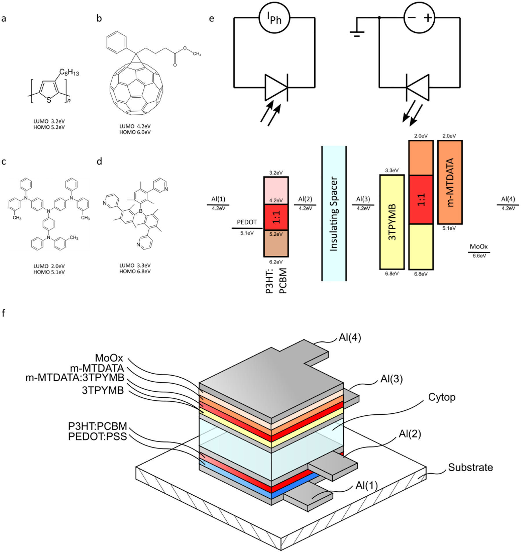
Chemical structure of P3HT (a), PC61BM (b), m-MTDATA (c) and 3TPYMB (d). Equivalent circuit and energy alignment of the Organic photodetector / OLED stack (e) and device schematic (f). For later reference the Al-electrodes are numbered Al(1) through Al(4).
We want to point out that the electrode Al(1) was chosen to be semi-transparent to enable measurements of the OLED by an external Si-detector and to ensure device functionality is in agreement with expectations. While almost all light will be absorbed by the OPD and only a small amount is coupled out to the Si-detector, this configuration allows for a direct comparison of the magneto-electroluminescence (MEL) measured on the same device. This allows evaluation of the effect of pinholes and stacking induced morphology non-idealities. However, in a later sensing application this first Al-layer would be chosen to be opaque to maximize the light absorption inside the OPD and minimize the fraction of light lost by out-coupling from the device.
Rigid as well as flexible substrates might be chosen in the future. Similar to other OLED and OPD or organic photovoltaic (OPV) technologies, devices will need an encapsulation to protect against environmental influences, in particular chemical degradation due to oxygen and water.48–52 In commercial applications for OLEDs, encapsulation and material selection has been solved to a point that hundreds of operation hours can be reached. Recent research has focused on flexible encapsulations and multilayer laminates / barrier stacks have shown remarkable stability for 1000 bending cycles and storage under 60 °C and 90% relative humidity for 50 days with negligible OLED degradation.53 However, for simplicity and proof of concept for our sensor we do not employ encapsulation and instead measure the devices inside a controlled N2 environment (glovebox) with O2 and H2O content of < 0.1ppm.
Electric & magnetic field characterization of the OLEDs
Before discussing the OPD/OLED magnetic field sensor we want to briefly discuss the electric and magnetic field dependence of the OLEDs in “normal” architecture on glass/ITO to establish a reference point for the luminescence and magnetic characteristics of the OLED emission layer. The current density-voltage-luminescence, J-V-L, characteristics of exemplary devices of this architecture are shown in Figure 2. All devices exhibit a very pronounced rectification behavior due to the large LUMO and HOMO offsets between m-MTDATA and 3TPYMB that yield extraordinary charge carrier blocking for electrons and holes at the anode and cathode respectively. Unlike much thicker devices of m-MTDATA:3TPYMB 1:1.2 stoichiometry reported by Wang et al. which exhibit a voltage and luminescence turn-on near 4 V,54 we observe a turn-on near 2 V, corresponding to slightly below the m-MTDATA HOMO – 3TPYMB LUMO gap of 2.2 eV and also below the contact potential difference between Al(3) and MoOx (~2.4 eV) and anticipated flatband conditions. This is in agreement with classic pnjunction expectations. With increasing bias we see a rapidly increasing luminescence, following a power law dependence L ~ J n whereas n = 4 decreases to 1 with increasing current through the device, see Figure S1. The maximum external quantum efficiency (EQE) of 0.13% is observed near 4V bias, corresponding to (6 to 7) mA/cm2. For larger biases the EQE drops as does the exponent n from n = 1 near 4 V to n = 0.5 around 6 V, indicating increased higher order recombination like Auger recombination within the device at those bias voltages. Shown in Figure 2 is the luminescence spectrum of the OLEDs which exhibits strong peak emission near 575 nm corresponding to m-MTDATA: 3TPYMB exciplex emission as reported by Wang et al.54 The luminescence spectrum does not exhibit a wavelength shift or change in shape with magnetic field for our devices, shown in inset of Figure 2c are measurements with and without a 200 mT B-field.
Figure 2 -.
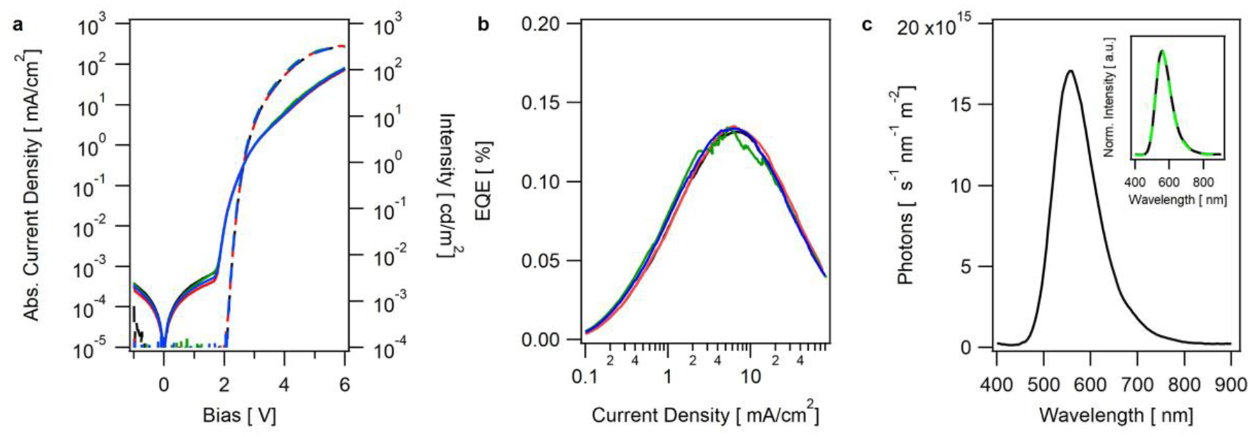
J-V-L-characteristics (a), EQE (b) and emission spectrum at 6 V, 75mA/cm2 (c) of typical m-MTDATA:3TPYMB 1:1 based OLEDs. Traces correspond to 4 individual devices on a substrate. The inset in (c) shows the peak normalized emission spectrum of the OLED with and without the presence of a 200 mT magnetic field (green).
In agreement with the earlier reports, we observe an MEL = [Lum(B)/Lum(B=0) – 1]·100% of up to 60% for constant bias in the as-prepared OLEDs. A large contribution of this astonishing response is due to a 20% decrease in magneto resistance, MR = [R(B)/R(B=0) – 1]·100%, which is also in agreement with Wang et. al. However, for constant current density operation the MEL-response is around 10% which is still significant (see Figure S2). The luminescence and MEL decreased upon current stressing, in contrast to the 1000% MEL response reported by Wang et al. for current conditioned OLEDs. This might be attributable to the significantly thinner emitter layer in our experiments. Shown in Figure 3 are the bias and magnetic field dependent MEL and MR. Note that a small asymmetry due to device degradation, particularly at larger forward biases and driving currents, can be observed that cannot be fully corrected by subtracting a linear background. However, this small degradation does not significantly alter the underlying line-shape.
Figure 3 -.
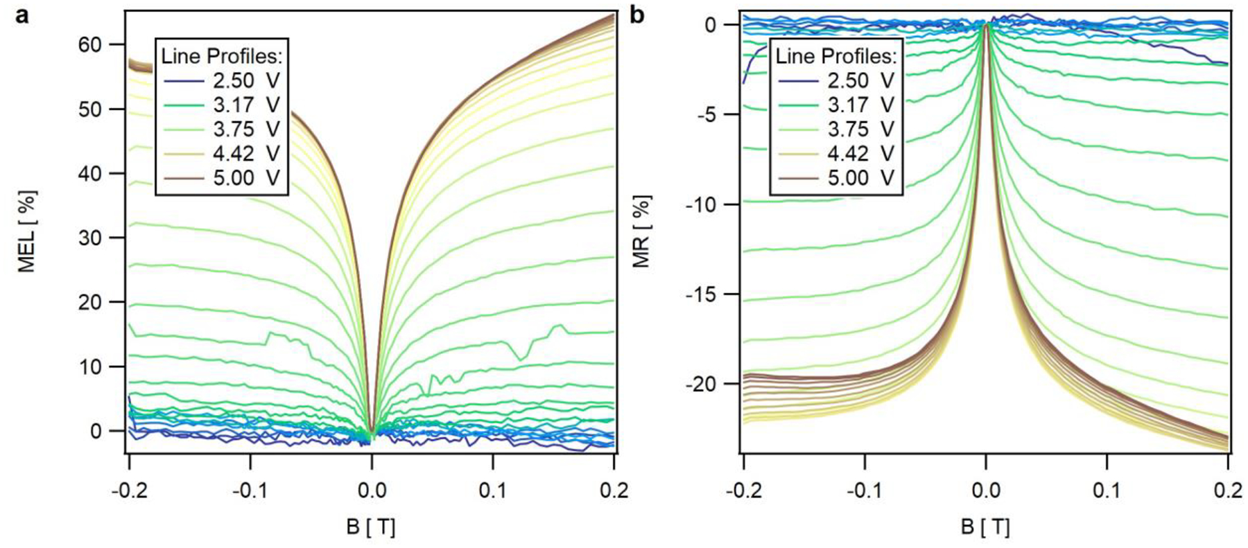
MEL- (a) and MR -response (b) as function of applied bias and magnetic field for a m-MTDATA:3TPYMB 1:1 based OLED on glass/ITO.
Both the MEL and MR exhibit slightly non-Lorentzian like line shapes around zero magnetic field that saturates for large magnetic fields, which is a common magnetic field effect (MFE) response of organic thin films. A Lorentzian line-shape, MFE ~ B2/(B2+B02), can be directly deduced from the Hamiltonian for hyperfine coupling dominated MFE.55 However, deviations from the Lorentzian line-shape can be observed and the MFE can be described by non-Lorentzian line-shapes given by MFE ~ B2/(ǀBǀ+B0) 2 or a superposition of both. In the case of zero-field splitting dominated MEL seen in tetracene, Alq3, or rubrene devices, a more “M” or “W”-like shape of the MEL can be observed that may or may not exhibit additional features due to crossings/anti-crossing of the eigenstates of zero-field spin Hamiltonian. As a plateau in the MEL and MR can be observed we can effectively rule out that zero-field-splitting significantly contributes to the MEL-response. Fitting the MEL- and MR-response to MFE ~ B2/(ǀBǀ+B0) 2 we extract a characteristic field, B0, of ≈ 5 mT and ≈ 7 mT for the MR and MEL response respectively. A graph of the extracted B0 values with applied bias is shown in Figure S3. We therefore attribute the MEL and MR response to the same underlying phenomenon. This is further supported by the observation that both MR and MEL onsets coincide at the same bias. It is worth noting that negative MC (positive MR) was observed in unipolar devices at low bias voltages17,56–58, suggesting that both charges are involved in our case.
Characterization of the OPD/OLED magnetic field sensor
In the following section, the results for the combined OPD/OLED magnetic field-sensor will be shown. Additional information on a sensor based on separated OPD and OLED, both in normal architecture on glass/ITO substrates, can be found in the Supplementary information. Here we note that the EQE of the OPD in the relevant wavelength range around the maximum of the OLED emission is > 40% compared to 55% - 65% for a Si-detector, Figure S4. Furthermore, no significant change in photocurrent with magnetic field and only a minor change of the magneto-conductance (< 0.5%) was observed, see Figure S5.
Shown in Figure 4 are the J-V-L-characteristics of the OPD/OLED layer stack. For reference purposes the luminescence signal as measured by a Si-detector on the outside of the device is shown as well. The device geometry was optimized for the layer stack such that no light is coupled out of the device without passing the OPD. Thus, light reaching the Si-detector already passed through the OPD and the semi-transparent electrodes Al(1) through Al(3). This leads to an approximately 100× smaller detectable signal by the Si-detector compared to the OLEDs characterized in the first section of this manuscript. In an optimized device no light will be coupled out of the device, as both the bottom, Al(1), and top, Al(4), electrode will be opaque and the OPD thickness increased to enhance absorption and performance. However, for investigative purposes we choose to work with a geometry that allows for some light “leaking” out of the device, as this allows us to quantitatively address the TADF emission layer.
Figure 4 -.
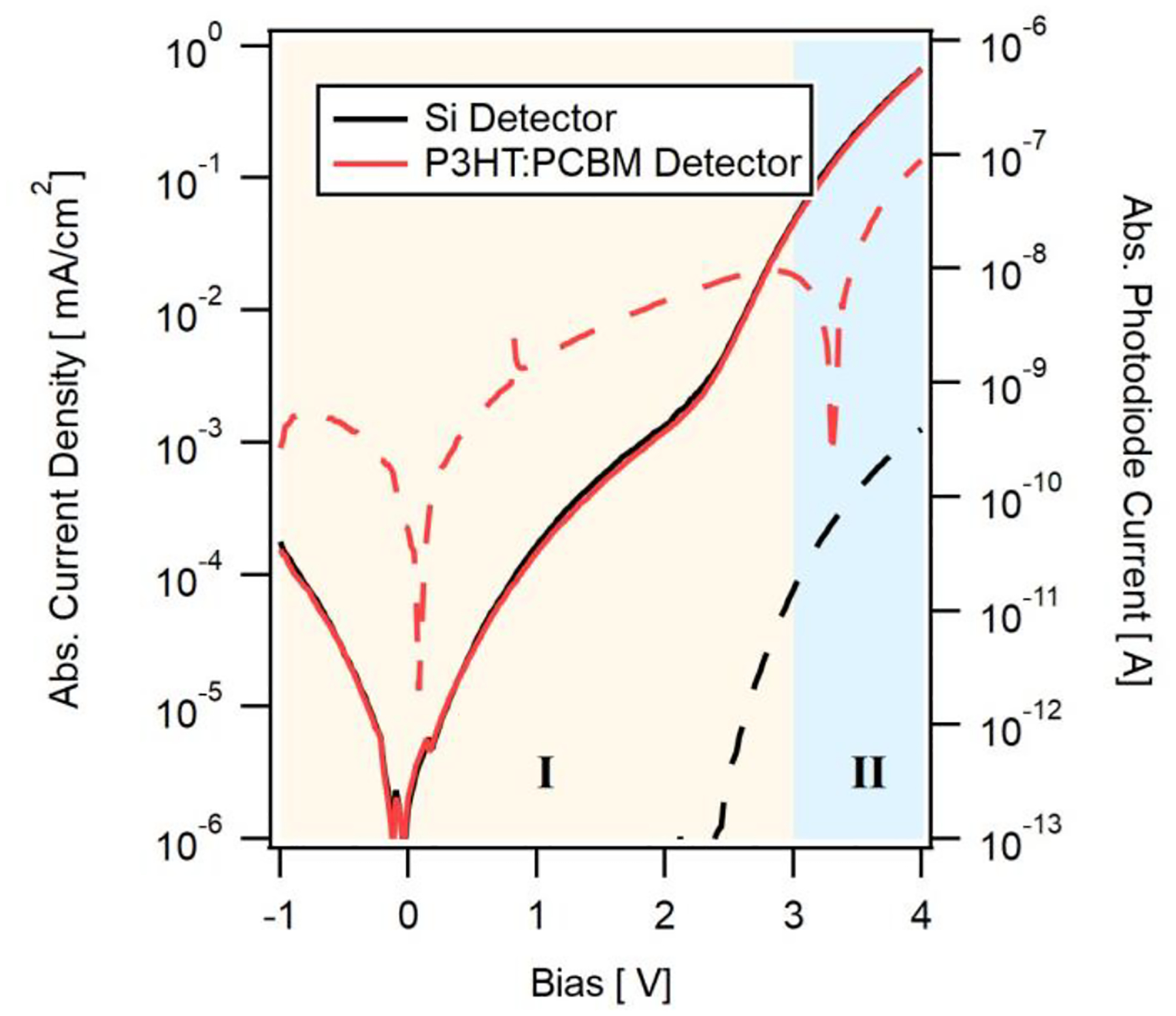
J-V-L-characteristics of the OPD/OLED layer stack. The luminescence measured by the OPD is shown in red broken lines, the luminescence as measured with a Si-detector on the outside the device is shown in black. Note the device geometry is not optimized for the Si-detection. Due to the absorption in the OPD layer and low transparency of the 20nm Al bottom electrode the detected signal by the Si-detector is several orders of magnitude smaller than in the reference TADF devices in the first section of the manuscript as well as compared to the OPD. Please note that the absolute of the photodetector current is plotted to allow for a comparison of the leakage currents and the photo-current due to luminesce over a large current range.
The turn-on voltage of the OLED emission as measured by the Si-detector slightly increased by 0.2 V as compared to the devices shown in Figure 2. This can be attributed to the significantly reduced outcoupling of the emitted light and detection floor which is limited by measurement noise. The J-V-characteristics of the OLED show a slightly less pronounced diode behavior compared to the devices in the first section of the manuscript, and an overall reduced current density. We attribute this to 2 factors, the first being an increased series resistance of the semi-transparent Al(3) electrode compared to the devices above, which besides the expected current loss also leads to a distribution of bias voltages with distance to the external contact point and washing out of the diode “knee”. And second, a slightly worse emitter morphology and film quality due to compiling defects and imperfections in each of the layers of the device stack. Despite the non-ideal behavior, the OLEDs show sufficient performance to demonstrate the sensor.
Unlike the ideal two region response of the Si-detector, constant low noise floor below emission turn-on followed by the above discussed bias dependent luminescence increase above the emission turn-on, the response of the OPD detector shows a strong bias dependence throughout all OLED biases. The region below the luminescence turn-on (< 2.2 V) and in the low luminescence region (< 3 V), region I (yellow shading), is dominated by electrical coupling of the OPD to the OLED. Due to pinholes in the insulating Cytop-spacer as well as some electrostatic coupling during the bias sweep, a non-linear background current can be measured. This current is positive which is the same sign as the OLED device current. Once luminescence from the OLED becomes significantly larger, the contribution of the generated photocurrent in the OPD becomes the dominating contribution to the OPD detector current, region (II, blue shading). Based on the chosen device geometry using a standard, non-inverted OPD layout the sign of the photocurrent is expected to be negative, and indeed between region (I) and (II) the current changes from negative to positive which makes us confident that region (II) is indeed where the photocurrent dominates the OPD response. The sign change in the OPD response occurs around 3.3 V in this case, whereas the prior local extrema in the OPD current signal can be observed at about 2.8 V and lines-up well with the turn-on of the electroluminescence as measured by the Si-detector. Note that we plot the absolute value of the detector current in Figure 4 to allow for a comparison of the currents over several orders of magnitude (log-scale). Shown in Figure S6 is the same data on a linear scale for the detector response.
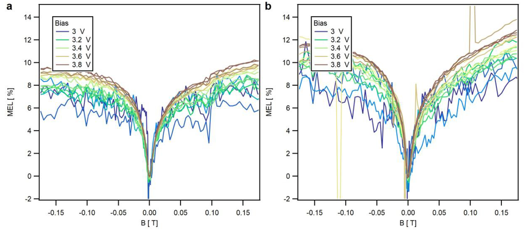
The following section will include a discussion of the MEL response of the OPD/OLED stack and subsequent device operation. Shown in Figure 5 are the response from the Si-detector and OPD in a side-by-side comparison, for an overlay of both datasets on the same graph please refer to Figure S7. Note measurements were performed in a sequential order where measurement resulted in slight device degradation, especially that of the P3HT:PCBM OPD. Shown in Figure S8 are J-V-L-characterizations of the device after each additional measurement. Note the bias at which the OPD sign changes shifts from 3.3 V prior the first MEL-map to 3.7 V after completion. To ensure reliable data, the MEL response measured by the integrated OPD was background corrected for the coupling between OPD and OLED, the uncorrected data is shown in Figure S9. About 10% MEL can be observed when measured with the Si-detector. The reduced magnitude of the MEL as compared to the OLED response reported in the first section of the manuscript might be due to the slightly worse layer quality in the increasingly complex device. However, both the internal OPD detector and external Si-detector show MEL responses that agree very well with each other.
Figure 5 -.
MEL-response as function of applied OLED bias and magnetic field for the OPD/OLED device measured with the Si-photodetector (a) and with the integrated OPD-detector (b). The MEL data measured by the OPD was background corrected.
Rather than the MEL response, the application relevant characteristics are the field sensitivity, which in this case is the derivation of the detector current S = dI/dB, and the detectivity which provides the noise floor and is the lowest magnetic field that can be measured. Sensitivities for different sensor types themselves cannot be compared easily. This is due to different measured state variables for different sensor types, e.g. voltage for Hall-sensors, resistance for MR based sensors, frequency for resonance based magnetometers10,59, etc. However, it provides for a way to evaluate the accessible field range, linearity and required readout electronics. For the fabricated OPD/OLED layer stacks the sensitivity at various bias voltages of the OLED is shown in Figure 6 for a magnetic field scan from −25 mT to 25 mT. The sensitivity shows a highly non-linear dependence which is comparable to those of magneto-resistive devices and expected from the Lorentzian like line shape of the underlying magnetic field response. The maximum sensitivity is about 0.15 nA/mT near a magnetic field of 3 mT to 4 mT. For comparison the sensitivity for an OLED on ITO glass at 4 V measured with a Si-detector is about an order of magnitude bigger with approximately 2 nA/mT.
Figure 6 -.
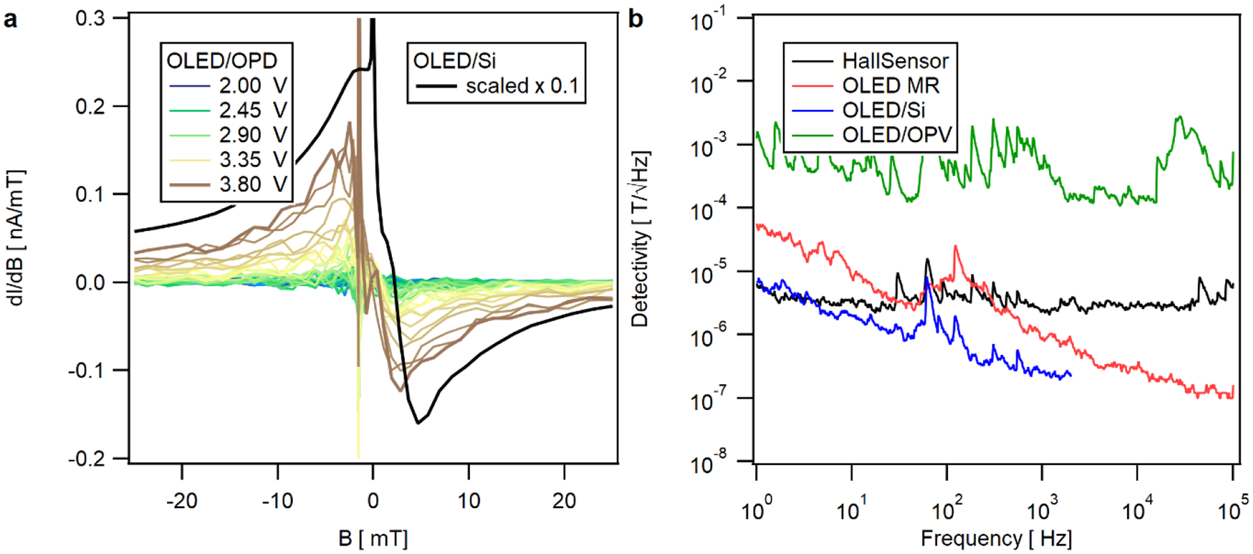
Sensitivity S = dI/dB as function of applied bias and magnetic field for the OPD/OLED device (a). Shown in (b) is the measured detectivity compared to a commercial Hall-sensor as well as to the detectivity that can be reached evaluating the MR and MEL with a Si detector of an OLED deposited on glass/ITO. No data smoothing or data correction was performed.
Also shown in Figure 6 is the detectivity that can be reached by our sensor setup and a Hall sensor. Currently high electric noise levels likely caused by coupling between the OPD and OLED sub-devices, and the low EQE of the monolithic device limit the detectivity to mT Hz 1/2, however noise data for a reference OLED on ITO glass measured using a Si-detector without magnetic shielding shows field detectivities comparable to those of a Hall-sensor (μT Hz −1/2) and below. Compared to the detectivity that can be achieved by utilizing the MR effect alone, the detectivity via the measurement of the MEL response using a good detector is one order of magnitude lower. This is in part due to the increased MEL response compared to the MR (Figure 3).
Finally, we want to provide an estimation on what detectivities could ultimately be reached upon further device optimization and that of the external measurement setup. Approximating the internal detectivity limit by the sum of all noise sources within the sensor represented by their respective noise spectral densities N in the status variable of the measurement:
In case of the OPD/OLED device the relevant noise sources are the detector noise of the photodiode which if reverse biased equals the “dark current shot noise” ~2qIs, and the noise of the light source. We assume that the emission noise is due to the driving current of the OLED device, which if sufficiently forward biased is again shot noise limited ~2qId · EQE, where we account for the fraction of emitted photons via the EQE of the OLED device. As Id is orders of magnitudes larger than the dark saturation current of the detector, the noise limit is dictated by the OLED emission such that we can give an upper estimate of 2× emission noise as a limit. Based on the values of the glass/ITO OLED at 4V forward bias with a driving current of Id ~1.6mA (experimental current density of 10 mA/cm2 , see Figure 2), EQE of 6·10−3 % and dI/dB = 1 nA/mT the detectivity limit thus would be about 3 nT/Hz −1/2. For comparison the detectivity for the same MR based device (shot noise ~ 2qId, dI/dB = 500 nA/mT) would be an order of magnitude bigger ~50 nT/Hz −1/2. Later estimate agrees with giant magnetoresistance based magnetic field sensors of similar magnitude in MR (~ 10%), e.g. ~100 nT Hz −1/2 at low frequencies and (0.1 – 10) nT Hz −1/2 at high frequencies.60,61 Thus pointing to the origin of the low detectivities in our preliminary data above in the external electronics for amplification and detection and not the core sensor itself.
Conclusion
In this study we have introduced a thin film magnetic field sensor based on a monolithic OPD/OLED layer stack based on the large magnetic field response of the OLED emission. We have shown that sensitivities and detectivities comparable to those of commercial Hall-sensors can be achieved and predict it will be exceeded with optimization. The field sensitivity for the monolithic stack was 0.15 nA/mT near a magnetic field of 3 mT to 4 mT. However, the detectivity was somewhat limited with 10−3 T·Hz−1/2. For comparison the sensitivity of OLEDs on ITO glass and measured by an external Si-detector is about an order of magnitude better with approximately 2 nA/mT and detectivity < 10−5 T·Hz−1/2, identical to what we measured for a Hall-sensor. This first proof of concept provides a promising reference point.
Device performance increase of the OPD/OLED-stack is expected by upscaling of the deposition processes and additional optimization. The EQE and MEL-change are well below the reported literature values for OLEDs based on the same TADF material, and so improvements to the fabrication of the OLED on the OPD surface will undoubtably result in better performance than the demonstration shown here. Recent studies of similar materials have shown large magnetic field effects of 10’s and even 100’s percent47,54,62–64, which allows for further optimization of the device by emitter selection and doping optimization. Furthermore, the detection component can be improved by replacing the P3HT based OPD with a detector layer with higher efficiency or one that shows a strong magnetic field response that can be used to compound field sensitivity.42 Assuming a luminescence change of the OLED on the order of 60 % a modest change in the detected photocurrent of 3% MFE would lead to compounded 65 % change of the overall detector-signal. This compounding sensitivity increase represents an inherent benefit of the monolithic stack compared to simpler MR based sensors, which only detect the change in a single active layer.
We envision that solution processed and evaporated devices may find use in traditional and non-traditional applications replacing Hall-sensors, GMR and TMR based sensors. One might envision medical applications, e.g. MCG, if detectivity limits can be improved to pT·Hz−1/2 and below. Additionally, the described layer stack might be operated with FETs in a bistable operation, Xue and Forrest,65 to form a magnetic switch. Combining these possibilities with printed electronics and flexible electronics makes it possible to integrate this sensor into electronic skin applications and existing OLED technologies.
Methods
Device Fabrication
The donor and acceptor materials 4,4′,4′′-Tris[phenyl(m-tolyl)amino]triphenylamine (m-MTDATA) and Tri[3-(3-pyridyl)mesityl]borane (3TPYMB), respectively, were purchased from Sigma Aldrich1 and used as received. Devices were deposited on commercially available patterned indium tin oxide (Thin Film Devices, Rs = 15 ohms/sq) or glass with evaporated Al electrodes. Substrates were cleaned via sonication in chloroform and isopropanol, followed by 15 min of ultraviolet/ozone treatment. PEDOT:PSS (Clevios AI4083) was spun at 3000 rpm and annealed 10min @ 120C under ambient conditions. P3HT:PCBM 1:1 was spun from a 40 mg/mL by weight solution under ambient conditions. The OPD was annealed at 150C inside a nitrogen filled GB after deposition of the Al electrodes. All metal films, MoOx, as well as m-MDATA and 3TPYMB were thermally evaporated using a Lesker deposition system at a base pressure of < 10−4 Pa connected to an N2 purged glovebox (<1 ppm H2O, O2). The layered architecture of the herein investigated devices was:
TADF OLEDs on ITO Glass: Glass/ITO/PEDOT:PSS/m-MTDATA(20 nm)/m-MTDATA:3TPYMB(1:1, 40 nm)/3TPYMB(5 nm)/Al(80 nm) Device Area as defined by the overlap between ITO and metal electrode was 4 mm2
OPD/OLED stack: Glass/Al(20 nm)/PEDOT:PSS/P3HT:PCBM(1:1)/Al(10 nm)/Cytop/Al(10 nm)/3TPYMB(10 nm)/m-MTDATA:3TPYMB(1:1, 40 nm)/m-MTDATA(20 nm)/MoOx(7.5 nm)/Al(40 nm) Device Area: 16 mm2
Device Characterization
Current density-Voltage-Luminescence, J-V-L, characteristics were measured using a Keithley 2636A source meter and Si-photodetector (Thorlabs SM1PD1B) placed on top the OLED devices. The dark current of the Si-photodetector was < 5 pA and relative luminescence curves have been corrected for a constant background obtained in the negative bias range. Measured photodiode currents were converted to luminance values via weighting of the OLED emission spectrum by the measured detector response and luminous function. In case of the OPD/OLED devices additional measurements were performed using the internal detector (OPD). In these cases, no correction to the obtained detector current were performed unless otherwise noted. Magneto-electroluminescence, MEL, was measured with the sample placed between the poles of an electromagnet, with the magnetic field vector perpendicular to the surface normal (in the plane of the substrate). The magnetic field was measured using a Hall probe. The maximum field strength was 175 mT. All measurements were performed inside a N2 purged glovebox (<1 ppm H2O, O2).
Supplementary Material
Acknowledgements
S.E. acknowledges support from the U.S. Department of Commerce, National Institute of Standards and Technology under the financial assistance award 70NANB17H305 and 70NANB21H058.
Footnotes
Certain commercial equipment, instruments, or materials are identified in this paper in order to specify the experimental procedure adequately. Such identification is not intended to imply recommendation or endorsement by the National Institute of Standards and Technology, nor is it intended to imply that the materials or equipment identified are necessarily the best available for the purpose.
Bibliography
- 1.Tokito S in 2018 IEEE 2nd Electron Devices Technology and Manufacturing Conference (EDTM). 260–261. [Google Scholar]
- 2.Krebs FC, Espinosa N, Hösel M, Søndergaard RR & Jørgensen M 25th Anniversary Article: Rise to Power – OPV-Based Solar Parks. Advanced Materials 26, 29–39 (2014). 10.1002/adma.201302031 [DOI] [PubMed] [Google Scholar]
- 3.Li B, Hou B & Amaratunga GAJ Indoor photovoltaics, The Next Big Trend in solution-processed solar cells. InfoMat 3, 445–459 (2021). 10.1002/inf2.12180 [DOI] [Google Scholar]
- 4.Miranda BHS, Corrêa L. d. Q., Soares GA, Martins JL, Lopes PL, Vilela ML, Rodrigues JF, Cunha TG, Vilaça R. d. Q., Castro-Hermosa S, Wouk L & Bagnis D Efficient fully roll-to-roll coated encapsulated organic solar module for indoor applications. Solar Energy 220, 343–353 (2021). 10.1016/j.solener.2021.03.025 [DOI] [Google Scholar]
- 5.Rogers JA, Bao Z, Baldwin K, Dodabalapur A, Crone B, Raju VR, Kuck V, Katz H, Amundson K, Ewing J & Drzaic P Paper-like electronic displays: Large-area rubber-stamped plastic sheets of electronics and microencapsulated electrophoretic inks. Proceedings of the National Academy of Sciences of the United States of America 98, 4835–4840 (2001). 10.1073/pnas.091588098 [DOI] [PMC free article] [PubMed] [Google Scholar]
- 6.Gelinck GH, Huitema HEA, van Veenendaal E, Cantatore E, Schrijnemakers L, van der Putten JBPH, Geuns TCT, Beenhakkers M, Giesbers JB, Huisman B-H, Meijer EJ, Benito EM, Touwslager FJ, Marsman AW, van Rens BJE & de Leeuw DM Flexible active-matrix displays and shift registers based on solution-processed organic transistors. Nature Materials 3, 106–110 (2004). 10.1038/nmat1061 [DOI] [PubMed] [Google Scholar]
- 7.Rogers JA & Bao Z Printed plastic electronics and paperlike displays. J. Polym. Sci. Pol. Chem 40, 3327–3334 (2002). 10.1002/pola.10405 [DOI] [Google Scholar]
- 8.Rich SI, Jiang Z, Fukuda K & Someya T Well-rounded devices: the fabrication of electronics on curved surfaces – a review. Materials Horizons (2021). 10.1039/D1MH00143D [DOI] [PubMed] [Google Scholar]
- 9.Veeraraghavan G, Nguyen TD, Sheng Y, Mermer O & Wohlgenannt M An 8 × 8 Pixel Array Pen-Input OLED Screen Based on Organic Magnetoresistance. IEEE Transactions on Electron Devices 54, 1571–1577 (2007). 10.1109/TED.2007.895240 [DOI] [Google Scholar]
- 10.Geng R, Mena A, Pappas WJ & McCamey DR Sub-micron spin-based magnetic field imaging with an organic light emitting diode. Nature Communications 14, 1441 (2023). 10.1038/s41467-023-37090-y [DOI] [PMC free article] [PubMed] [Google Scholar]
- 11.Heikenfeld J, Jajack A, Rogers J, Gutruf P, Tian L, Pan T, Li R, Khine M, Kim J, Wang J & Kim J Wearable sensors: modalities, challenges, and prospects. Lab on a Chip 18, 217–248 (2018). 10.1039/C7LC00914C [DOI] [PMC free article] [PubMed] [Google Scholar]
- 12.Yokota T, Zalar P, Kaltenbrunner M, Jinno H, Matsuhisa N, Kitanosako H, Tachibana Y, Yukita W, Koizumi M & Someya T Ultraflexible organic photonic skin. Science Advances 2, e1501856 10.1126/sciadv.1501856 [DOI] [PMC free article] [PubMed] [Google Scholar]
- 13.Leleux P, Badier J-M, Rivnay J, Bénar C, Hervé T, Chauvel P & Malliaras GG Conducting Polymer Electrodes for Electroencephalography. Advanced Healthcare Materials 3, 490–493 (2014). 10.1002/adhm.201300311 [DOI] [PubMed] [Google Scholar]
- 14.Lochner CM, Khan Y, Pierre A & Arias AC All-organic optoelectronic sensor for pulse oximetry. Nature Communications 5, 5745 (2014). 10.1038/ncomms6745 [DOI] [PubMed] [Google Scholar]
- 15.Khan MA, Sun J, Li B, Przybysz A & Kosel J Magnetic sensors-A review and recent technologies. Engineering Research Express 3, 022005 (2021). 10.1088/2631-8695/ac0838 [DOI] [Google Scholar]
- 16.Tsurumi J, Matsui H, Kubo T, Häusermann R, Mitsui C, Okamoto T, Watanabe S & Takeya J Coexistence of ultra-long spin relaxation time and coherent charge transport in organic single-crystal semiconductors. Nature Physics 13, 994–998 (2017). 10.1038/nphys4217 [DOI] [Google Scholar]
- 17.Geng R, Daugherty TT, Do K, Luong HM & Nguyen TD A review on organic spintronic materials and devices: I. Magnetic field effect on organic light emitting diodes. Journal of Science: Advanced Materials and Devices 1, 128–140 (2016). 10.1016/j.jsamd.2016.05.002 [DOI] [Google Scholar]
- 18.Yu ZG Spin-Orbit Coupling, Spin Relaxation, and Spin Diffusion in Organic Solids. Physical Review Letters 106, 106602 (2011). 10.1103/PhysRevLett.106.106602 [DOI] [PubMed] [Google Scholar]
- 19.Nuccio L, Willis M, Schulz L, Fratini S, Messina F, D’Amico M, Pratt FL, Lord JS, McKenzie I, Loth M, Purushothaman B, Anthony J, Heeney M, Wilson RM, Hernández I, Cannas M, Sedlak K, Kreouzis T, Gillin WP, Bernhard C & Drew AJ Importance of Spin-Orbit Interaction for the Electron Spin Relaxation in Organic Semiconductors. Physical Review Letters 110, 216602 (2013). 10.1103/PhysRevLett.110.216602 [DOI] [PubMed] [Google Scholar]
- 20.Singh-Rachford TN & Castellano FN Photon upconversion based on sensitized triplet–triplet annihilation. Coordination Chemistry Reviews 254, 2560–2573 (2010). 10.1016/j.ccr.2010.01.003 [DOI] [Google Scholar]
- 21.Kondakov DY Triplet–triplet annihilation in highly efficient fluorescent organic light-emitting diodes: current state and future outlook. Philosophical Transactions of the Royal Society A: Mathematical, Physical and Engineering Sciences 373, 20140321 (2015). 10.1098/rsta.2014.0321 [DOI] [PubMed] [Google Scholar]
- 22.Xiang C, Peng C, Chen Y & So F Origin of Sub-Bandgap Electroluminescence in Organic Light-Emitting Diodes. Small 11, 5439–5443 (2015). 10.1002/smll.201501355 [DOI] [PubMed] [Google Scholar]
- 23.Pandey AK Highly efficient spin-conversion effect leading to energy up-converted electroluminescence in singlet fission photovoltaics. 5, 7787 (2015). 10.1038/srep07787 [DOI] [PMC free article] [PubMed] [Google Scholar]
- 24.Chen Q, Jia W, Chen L, Yuan D, Zou Y & Xiong Z Determining the Origin of Half-bandgap-voltage Electroluminescence in Bifunctional Rubrene/C60 Devices. Scientific Reports 6, 25331 (2016). 10.1038/srep25331 [DOI] [PMC free article] [PubMed] [Google Scholar]
- 25.Engmann S, Barito AJ, Bittle EG, Giebink NC, Richter LJ & Gundlach DJ Higher order effects in organic LEDs with sub-bandgap turn-on. Nature Communications 10, 227 (2019). 10.1038/s41467-018-08075-z [DOI] [PMC free article] [PubMed] [Google Scholar]
- 26.Engmann S, Barito AJ, Bittle EG, Giebink NC, Richter LJ & Gundlach DJ Reply to: Triplet-triplet annihilation in rubrene/C60 OLEDs with electroluminescence turn-on breaking the thermodynamic limit. Nature Communications 10, 4684 (2019). 10.1038/s41467-019-12598-4 [DOI] [PMC free article] [PubMed] [Google Scholar]
- 27.Johnson RC & Merrifield RE Effects of Magnetic Fields on the Mutual Annihilation of Triplet Excitons in Anthracene Crystals. Physical Review B 1, 896–902 (1970). 10.1103/PhysRevB.1.896 [DOI] [Google Scholar]
- 28.Johnson RC, Merrifield RE, Avakian P & Flippen RB Effects of Magnetic Fields on the Mutual Annihilation of Triplet Excitons in Molecular Crystals. Physical Review Letters 19, 285–287 (1967). 10.1103/PhysRevLett.19.285 [DOI] [Google Scholar]
- 29.Merrifield RE Magnetic effects on triplet exciton interactions. Pure and Applied Chemistry 27, 481–498 (1971). 10.1351/pac197127030481 [DOI] [Google Scholar]
- 30.Timmel CR, Till U, Brocklehurst B, McLauchlan KA & Hore PJ Effects of weak magnetic fields on free radical recombination reactions. Molecular Physics 95, 71–89 (1998). 10.1080/00268979809483134 [DOI] [Google Scholar]
- 31.Wang S, Pratama FR, Ukhtary MS & Saito R Independent degrees of freedom in two-dimensional materials. Physical Review B 101, 081414 (2020). 10.1103/PhysRevB.101.081414 [DOI] [Google Scholar]
- 32.Wang S, Ukhtary MS & Saito R Strain effect on circularly polarized electroluminescence in transition metal dichalcogenides. Physical Review Research 2, 033340 (2020). 10.1103/PhysRevResearch.2.033340 [DOI] [Google Scholar]
- 33.Jang H-J, Bittle EG, Zhang Q, Biacchi AJ, Richter CA & Gundlach DJ Electrical Detection of Singlet Fission in Single Crystal Tetracene Transistors. ACS Nano 13, 616–623 (2019). 10.1021/acsnano.8b07625 [DOI] [PMC free article] [PubMed] [Google Scholar]
- 34.Walker BJ, Musser AJ, Beljonne D & Friend RH Singlet exciton fission in solution. Nature Chemistry 5, 1019–1024 (2013). 10.1038/nchem.1801 [DOI] [PubMed] [Google Scholar]
- 35.Stern HL, Musser AJ, Gelinas S, Parkinson P, Herz LM, Bruzek MJ, Anthony J, Friend RH & Walker BJ Identification of a triplet pair intermediate in singlet exciton fission in solution. Proceedings of the National Academy of Sciences 112, 7656–7661 (2015). 10.1073/pnas.1503471112 [DOI] [PMC free article] [PubMed] [Google Scholar]
- 36.Yong CK, Musser AJ, Bayliss SL, Lukman S, Tamura H, Bubnova O, Hallani RK, Meneau A, Resel R, Maruyama M, Hotta S, Herz LM, Beljonne D, Anthony JE, Clark J & Sirringhaus H The entangled triplet pair state in acene and heteroacene materials. Nature Communications 8, 15953 (2017). 10.1038/ncomms15953 [DOI] [PMC free article] [PubMed] [Google Scholar]
- 37.He SJ & Lu ZH Ultralow-voltage Auger-electron-stimulated organic light-emitting diodes. PHOTOE 6, 12 (2016). 10.1117/1.jpe.6.036001 [DOI] [Google Scholar]
- 38.Pandey AK & Nunzi J-M Upconversion injection in rubrene/perylene-diimide-heterostructure electroluminescent diodes. Applied Physics Letters 90, 263508 (2007). 10.1063/1.2752540 [DOI] [Google Scholar]
- 39.Han S, Yuan Y & Lu Z-H Highly efficient organic light-emitting diodes with metal/fullerene anode. Journal of Applied Physics 100, 074504 (2006). 10.1063/1.2354319 [DOI] [Google Scholar]
- 40.Qiao X, Yuan P, Ma D, Ahamad T & Alshehri SM Electrical pumped energy up-conversion: A non-linear electroluminescence process mediated by triplet-triplet annihilation. Organic Electronics 46, 1–6 (2017). 10.1016/j.orgel.2017.03.020 [DOI] [Google Scholar]
- 41.Masui K, Nakanotani H & Adachi C Analysis of exciton annihilation in high-efficiency sky-blue organic light-emitting diodes with thermally activated delayed fluorescence. Organic Electronics 14, 2721–2726 (2013). 10.1016/j.orgel.2013.07.010 [DOI] [Google Scholar]
- 42.Bittle EG, Engmann S, Thorley K & Anthony J Measuring the impact of spin-triplet exciton orientation on photocurrent in an organic transistor. Journal of Materials Chemistry C 9, 11809–11814 (2021). 10.1039/D1TC01539G [DOI] [Google Scholar]
- 43.Engmann S, Bittle EG, Richter LJ, Hallani RK, Anthony JE & Gundlach DJ The role of orientation in the MEL response of OLEDs. Journal of Materials Chemistry C 9, 10052–10064 (2021). 10.1039/D1TC00314C [DOI] [PMC free article] [PubMed] [Google Scholar]
- 44.Duc Nguyen T, Sheng Y, Rybicki JE & Wohlgenannt M Magnetoconductivity and magnetoluminescence studies in bipolar and almost hole-only sandwich devices made from films of a π-conjugated molecule. Science and Technology of Advanced Materials 9, 024206 (2008). 10.1088/1468-6996/9/2/024206 [DOI] [PMC free article] [PubMed] [Google Scholar]
- 45.Wohlgenannt M, Flatté ME, Harmon NJ, Wang F, Kent AD & Macià F Singlet-to-triplet interconversion using hyperfine as well as ferromagnetic fringe fields. Philosophical Transactions of the Royal Society A: Mathematical, Physical and Engineering Sciences 373 (2015). 10.1098/rsta.2014.0326 [DOI] [PMC free article] [PubMed] [Google Scholar]
- 46.Chen Y, Jia W, Xiang J, Yuan D, Chen Q, Chen L & Xiong Z Identify triplet-charge interaction in rubrene-based diodes using magneto-conductance: Coexistence of dissociation and scattering channels. Organic Electronics 39, 207–213 (2016). 10.1016/j.orgel.2016.10.006 [DOI] [Google Scholar]
- 47.Bai JW, Chen P, Lei YL, Zhang Y, Zhang QM, Xiong ZH & Li F Studying singlet fission and triplet fusion by magneto-electroluminescence method in singlet–triplet energy-resonant organic light-emitting diodes. Organic Electronics 15, 169–174 (2014). 10.1016/j.orgel.2013.11.012 [DOI] [Google Scholar]
- 48.Joergensen M, Norrman K & Krebs FC Stability/degradation of polymer solar cells. Solar Energy Materials and Solar Cells 92, 686–714 (2008). 10.1016/j.solmat.2008.01.005 [DOI] [Google Scholar]
- 49.Manceau M, Gaume J, Rivaton A, Gardette J-L, Monier G & Bideux L Further insights into the photodegradation of poly(3-hexylthiophene) by means of X-ray photoelectron spectroscopy. Thin Solid Films 518, 7113–7118 (2010). 10.1016/j.orgel.2012.03.018 [DOI] [Google Scholar]
- 50.Zimmermann B, Wuerfel U & Niggemann M Longterm stability of efficient inverted P3HT:PCBM solar cells. Solar Energy Materials and Solar Cells 93, 491–496 (2009). 10.1016/j.solmat.2008.12.022 [DOI] [Google Scholar]
- 51.Chambon S, Manceau M, Firon M, Cros S, Rivaton A & Gardette J-L Photo-oxidation in an 18O2 atmosphere: A powerful tool to elucidate the mechanism of UV-visible light oxidation of polymers - Application to the photodegradation of MDMO-PPV. Polymer 49, 3288–3294 (2008). 10.1016/j.polymer.2008.04.001 [DOI] [Google Scholar]
- 52.Lee S, Ha H, Lee JY, Shon HK, Lee TG, Suh MC & Park Y Degradation Mechanism of Solution-Processed Organic Light-Emitting Diodes: Sputter Depth-Profile Study. Applied Surface Science 564, 150402 (2021). 10.1016/j.apsusc.2021.150402 [DOI] [Google Scholar]
- 53.Kang KS, Jeong SY, Jeong EG & Choi KC Reliable high temperature, high humidity flexible thin film encapsulation using Al2O3/MgO nanolaminates for flexible OLEDs. Nano Research 13, 2716–2725 (2020). 10.1007/s12274-020-2915-5 [DOI] [Google Scholar]
- 54.Wang Y, Sahin-Tiras K, Harmon NJ, Wohlgenannt M & Flatté ME Immense Magnetic Response of Exciplex Light Emission due to Correlated Spin-Charge Dynamics. Physical Review X 6, 011011 (2016). 10.1103/PhysRevX.6.011011 [DOI] [Google Scholar]
- 55.Sheng Y, Nguyen TD, Veeraraghavan G, Mermer Ö, Wohlgenannt M, Qiu S & Scherf U Hyperfine interaction and magnetoresistance in organic semiconductors. Physical Review B 74, 045213 (2006). 10.1103/PhysRevB.74.045213 [DOI] [Google Scholar]
- 56.Bloom FL, Wagemans W, Kemerink M & Koopmans B Separating Positive and Negative Magnetoresistance in Organic Semiconductor Devices. Physical Review Letters 99, 257201 (2007). 10.1103/PhysRevLett.99.257201 [DOI] [PubMed] [Google Scholar]
- 57.Wang FJ, Bässler H & Valy Vardeny Z Magnetic Field Effects in π-Conjugated Polymer-Fullerene Blends: Evidence for Multiple Components. Physical Review Letters 101, 236805 (2008). 10.1103/PhysRevLett.101.236805 [DOI] [PubMed] [Google Scholar]
- 58.Nguyen TD, Gautam BR, Ehrenfreund E & Vardeny ZV Magnetoconductance Response in Unipolar and Bipolar Organic Diodes at Ultrasmall Fields. Physical Review Letters 105, 166804 (2010). 10.1103/PhysRevLett.105.166804 [DOI] [PubMed] [Google Scholar]
- 59.Baker WJ, Ambal K, Waters DP, Baarda R, Morishita H, van Schooten K, McCamey DR, Lupton JM & Boehme C Robust absolute magnetometry with organic thin-film devices. Nature Communications 3, 898 (2012). 10.1038/ncomms1895 [DOI] [PMC free article] [PubMed] [Google Scholar]
- 60.Davies JE, Watts JD, Novotny J, Huang D & Eames PG Magnetoresistive sensor detectivity: A comparative analysis. Applied Physics Letters 118, 062401 (2021). 10.1063/5.0038187 [DOI] [Google Scholar]
- 61.Weitensfelder H, Brueckl H, Satz A, Pruegl K, Zimmer J, Luber S, Raberg W, Abert C, Bruckner F, Bachleitner-Hofmann A, Windl R & Suess D Comparison of Sensitivity and Low-Frequency Noise Contributions in Giant-Magnetoresistive and Tunneling-Magnetoresistive Spin-Valve Sensors with a Vortex-State Free Layer. Physical Review Applied 10, 054056 (2018). 10.1103/PhysRevApplied.10.054056 [DOI] [Google Scholar]
- 62.Ling Y, Lei Y, Zhang Q, Chen L, Song Q & Xiong Z Large magneto-conductance and magneto-electroluminescence in exciplex-based organic light-emitting diodes at room temperature. Applied Physics Letters 107, 213301 (2015). 10.1063/1.4936205 [DOI] [Google Scholar]
- 63.Mermer Ö, Veeraraghavan G, Francis TL, Sheng Y, Nguyen DT, Wohlgenannt M, Köhler A, Al-Suti MK & Khan MS Large magnetoresistance in nonmagnetic π-conjugated semiconductor thin film devices. Physical Review B 72, 205202 (2005). 10.1103/PhysRevB.72.205202 [DOI] [Google Scholar]
- 64.Xiong ZH, Wu D, Valy Vardeny Z & Shi J Giant magnetoresistance in organic spin-valves. Nature 427, 821–824 (2004). 10.1038/nature02325 [DOI] [PubMed] [Google Scholar]
- 65.Xue J & Forrest SR Organic optical bistable switch. Applied Physics Letters 82, 136–138 (2002). 10.1063/1.1533116 [DOI] [Google Scholar]
Associated Data
This section collects any data citations, data availability statements, or supplementary materials included in this article.