

Abstract

Interlayer excitons in transition-metal dichalcogenide heterobilayers combine high binding energy and valley-contrasting physics with a long optical lifetime and strong dipolar character. Their permanent electric dipole enables electric-field control of the emission energy, lifetime, and location. Device material and geometry impact the nature of the interlayer excitons via their real- and momentum-space configurations. Here, we show that interlayer excitons in MoS2/MoSe2 heterobilayers are formed by charge carriers residing at the Brillouin zone edges, with negligible interlayer hybridization. We find that the moiré superlattice leads to the reversal of the valley-dependent optical selection rules, yielding a positively valued g-factor and cross-polarized photoluminescence. Time-resolved photoluminescence measurements reveal that the interlayer exciton population retains the optically induced valley polarization throughout its microsecond-long lifetime. The combination of a long optical lifetime and valley polarization retention makes MoS2/MoSe2 heterobilayers a promising platform for studying fundamental bosonic interactions and developing excitonic circuits for optical information processing.
Keywords: layered materials heterostructures, transition-metal dichalcogenides, interlayer excitons, moiré superlattice, valley polarization, Stark shift, photoluminescence
Layered materials heterostructures (LMHs) comprising monolayer transition-metal dichalcogenides (1L-TMDs) are promising platforms for optoelectronics1−4 and quantum technology5 as they combine optically addressable spin and valley degrees of freedom6−8 with unique tunability through the choice of material combination9−11 and rotational alignment.12−14 TMD heterobilayers have drawn particular interest due to their ability to host interlayer excitons (iXs)15,16 which offer lifetime approaching 200 μs,17 strong repulsive dipolar interaction,18,19 and high sensitivity to rotational alignment,20−22 strain,17,23 and electric24 and magnetic25 fields. Different TMD combinations give rise to iX with drastically different properties, including oscillator strength,26,27 center-of-mass momentum,20,21 and degree of interlayer hybridization.19,22 Of the plethora of possible TMD combinations, the majority of research effort focused on 1L-MoSe2/1L-WSe227−30 and 1L-WS2/1L-WSe2.31−33 For other material combinations, key aspects of the iX nature, such as real- and momentum-space configuration, remain elusive due to the complexity of the underlying physics.
In this work, we investigate iX in 1L-MoS2/1L-MoSe2 using polarization-resolved magneto-photoluminescence spectroscopy. We find that iX photoluminescence (PL) is visible only in devices with relative twist angle less than 5°. This indicates that the constituent iX charge carriers reside at the edges of the Brillouin zone. We study the iX PL response to out-of-plane electric and magnetic fields and show that iX is formed by charge carriers at the ±K valleys with negligible degree of interlayer hybridization. Our time- and polarization-resolved PL measurements reveal microsecond-scale retention of optically induced valley polarization, demonstrating the potential of 1L-MoS2/1L-MoSe2 for opto-valleytronic applications.
Figure 1a shows an optical microscope image of one of our electric-field-tunable 1L-MoS2/1L-MoSe2. The hexagonal boron nitride (hBN) layers provide a flat and clean dielectric environment for 1L-MoS2/1L-MoSe2, and the transparent few-layer graphene (FLG) top and bottom gates allow optical measurements under an out-of-plane electric field. Each of the eight devices is fabricated using deterministic mechanical transfer,34,35 with constituent monolayers obtained through micromechanical exfoliation of bulk TMD crystals prepared by flux zone growth. Thickness and quality of constituent layers are characterized using Raman36 and PL spectroscopy (see Methods and Supporting Information Figures S1, S2). Figure 1b presents a schematic of the type-II alignment of electronic bands within 1L-MoS2/1L-MoSe2, with conduction-band minimum (valence-band maximum) occurring in 1L-MoS2 (1L-MoSe2).37,38 The type-II band alignment leads to interlayer charge separation and the formation of iX, with PL lower in energy compared to the intralayer PL of the constituent monolayers. The devices offer a range of twist angles between the 1L-TMD θ, enabling the investigation of iX momentum-space configuration. Figure 1c compares room-temperature (RT) PL spectra of two devices with θ = 1° (top) and θ = 28° (bottom). We identify θ using polarization-resolved second-harmonic generation (SHG) (Figure 1d) and note that our measurements do not allow us to distinguish parallel from antiparallel alignment between monolayers (Supporting Information Figure S3). Both devices show PL peaks corresponding to the A exciton in 1L-MoSe2 (1L-MoSe2 XA) at 1.55 eV and the A and B excitons in 1L-MoS2 (1L-MoS2 XA and XB) at 1.85 and 2.0 eV, respectively.39,40 Crucially, the iX PL peak at ∼1.3 eV is visible only in the device with θ = 1°. Of the eight devices with θ ranging from 1° to 28°, only those with θ ≤ 5° reveal the iX PL peak at RT (Supporting Information Figure S4), consistent with ref (41). Thus, close rotational alignment is critical for the observation of iX in 1L-MoS2/1L-MoSe2.
Figure 1.
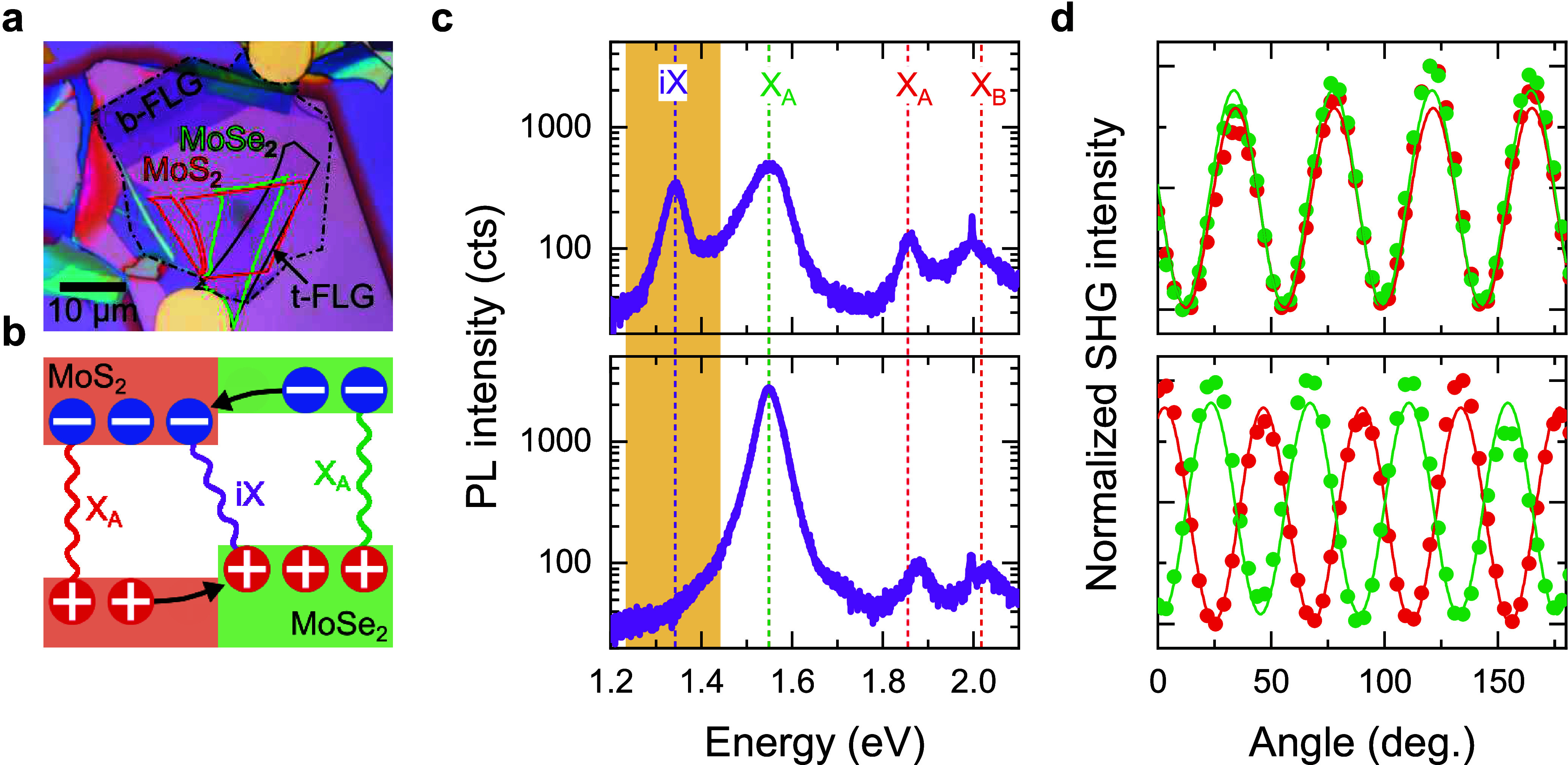
iX in 1L-MoS2/1L-MoSe2. (a) Optical microscope image of an electrically tunable 1L-MoS2/1L-MoSe2 device. 1L-MoS2 and 1L-MoSe2 regions are outlined in red and green, respectively. Solid (dashed) black lines show the position of top (bottom) FLG gates. (b) Schematic band alignment of 1L-MoS2 and 1L-MoSe2. (c) RT PL spectra recorded in two devices with different θ. The closely rotationally aligned device (top panel, θ = 1°) shows intralayer 1L-MoS2 B and A excitons and 1L-MoSe2 A exciton peaks, as well as an iX peak appearing in a lower-energy range (highlighted in copper), not visible in the PL spectrum of the strongly misaligned device (bottom panel, θ = 28°). (d) Polarization-resolved SHG intensity recorded in isolated (red) 1L-MoS2 and (green) 1L-MoSe2 regions of the two devices, confirming θ = 1° (top) and θ = 28° (bottom).
The ∼3.7% mismatch in lattice constants of 1L-MoS2 and 1L-MoSe242 eliminates θ dependence of the interlayer distance as an underlying source of this behavior.43 Instead, the high sensitivity of the iX PL intensity to θ indicates that iX is formed by the charge carriers residing in valleys at the edges of the Brillouin zone (BZ). Homo- and heterobilayers where at least one of the charge carriers resides at the Γ valley at the BZ center of display iX PL throughout the entire θ range, as the momentum-space separation between electron and hole remains unchanged.21,44,45 In contrast, in heterobilayers where both constituent charges reside at the BZ edges, large momentum-space separation of electron and hole suppresses radiative recombination of iX in devices with θ away from 0 or 60°,13,20 consistent with our observations.
Our device structure enables control of doping and the electric field independently. We use this to identify the real-space configuration of iX by studying its response to an out-of-plane electric field in the neutral regime. We note that the doping dependence of iX emission is reminiscent of what is observed in 1L-WS2/1L-WSe219,46,47 (Supporting Information Figure S5). Figure 2a presents the normalized iX PL spectrum recorded as a function of electric field at 4K. The iX PL energy shifts linearly with a rate ∼0.31 eV nm V–1 and can be tuned over a 144-meV range within the gate tuning limits of our device. We find an average tuning response across three devices of ∼0.30 eV nm V–1, yielding an average dipole size ∼0.55(3) nm19,24 (Supporting Information Figure S6), in good agreement with the ∼0.6 nm separation between the layers.48 A similar dipole size was observed in 1L-MoSe2/1L-WSe219, where iX is formed by nonhybridized electrons and holes, while MoSe2 homobilayers show a reduced dipole size of 0.26 nm due to charge-carrier hybridization.49 Comparatively, our results suggest negligible interlayer hybridization for our devices.
Figure 2.
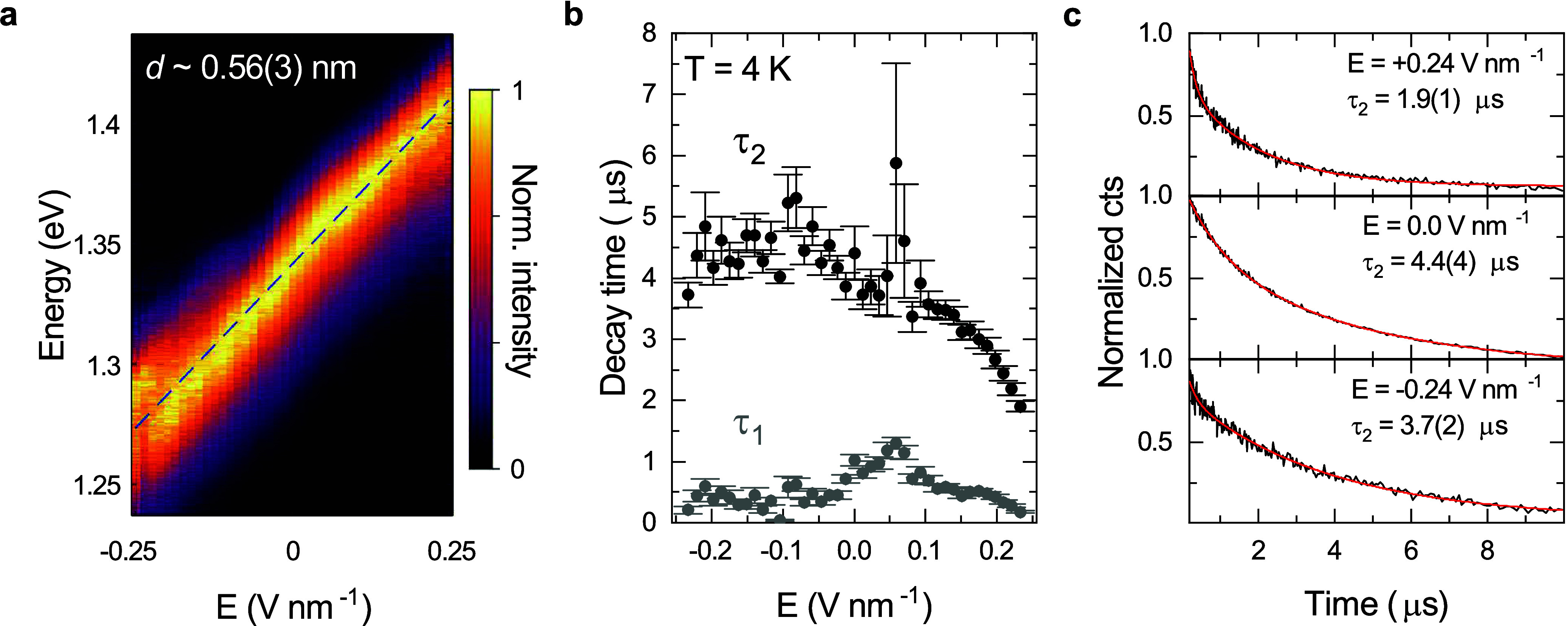
Electric field tuning of iX. (a) Normalized iX PL under out-of-plane electric field. The iX PL energy shows a linear shift with slope ∼0.31 eV nm V–1, corresponding to a dipole size of d = 0.56(3) nm, closely matching the expected interlayer distance. (b) Variation of iX PL decay time as a function of electric field. Gray and black circles correspond to fast (τ1) and slow (τ2) time constants, respectively. (c) PL decay acquired at +0.24, 0, and −0.24 V nm–1. Red curves are biexponential fits to the data.
Figure 2b shows the iX PL decay time constants as a function of electric field. We extract these constants from a biexponential fit to the time-resolved PL. Figure 2c presents examples of a PL decay trace recorded at three applied field values along with their corresponding fit curves. We observe a microsecond-long iX lifetime, with a fast time constant τ1 = 1.0(1) μs and a slow time constant τ2 = 4.4(4) μs at zero electric field—an order of magnitude longer than typical lifetimes of 10–100 ns reported for 1L-MoSe2/1L-WSe2.13 The slow time constant in other devices ranges from 0.1 to 3.0 μs (Supporting Information Figure S7). The variability of PL lifetime measured across different devices supports the assignment of this time scale to iX PL, rather than defect-bound PL. The fast time constant is mostly field-independent, except for ∼0.06 V nm–1, where it increases to 1.3 μs. Shortening of τ1 for the electric field away from this value is likely caused by inadvertent electrostatic doping induced by a slight asymmetry in the thicknesses of the bottom and top dielectric layers. The slow time constant τ2 shows a gradual decrease with increasing electric field, consistent with a change in radiative lifetime due to a field-induced variation of electron–hole separation. For electric field antiparallel to the iX electric dipole moment, the separation between the two charge carriers is reduced, leading to an increased probability of radiative recombination. The opposite process takes place for parallel field alignment. That said, the PL decay time remains slow (τ1 ≥ 0.04 μs, τ2 ≥ 1.9 μs) throughout the entire field-tuning range.
We use polarization-resolved magneto-PL spectroscopy to identify the valley configuration of iX. Figure 3a shows iX PL spectra recorded using right circularly polarized (σ+), 1.94 eV excitation as a function of applied out-of-plane magnetic field B ranging from −6 to 6 T; blue (red) curves correspond to PL with σ+ (σ–) polarization. The iX PL remains cross-polarized with respect to the excitation laser throughout the entire magnetic field range. Two distinct mechanisms are known to give rise to this behavior in TMD heterobilayers: 1) directional intervalley scattering50; 2) moiré-induced reversal of the valley-dependent optical selection rules.51
Figure 3.
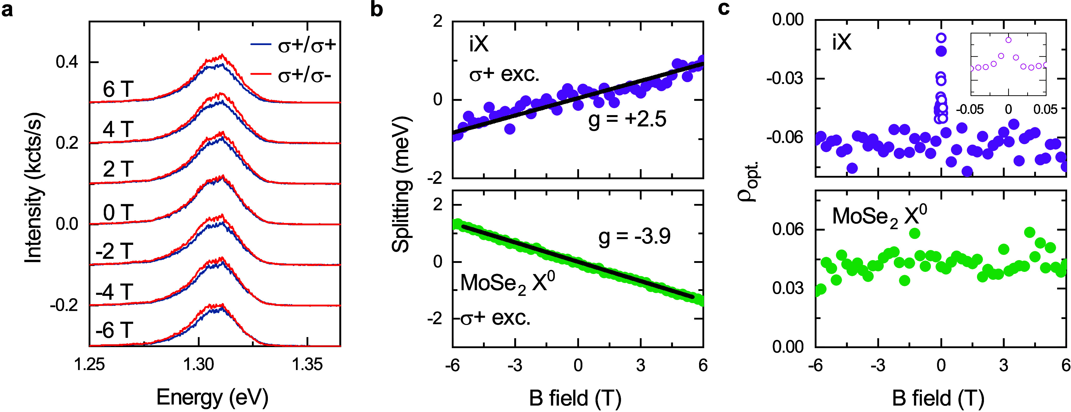
Magneto-PL spectroscopy of iX. (a) Helicity-resolved iX PL spectra recorded under out-of-plane magnetic field ranging from −6 to 6 T using σ+ polarized 1.94 eV optical excitation; blue (red) curves correspond to PL with σ+ (σ–) polarization. (b) Energy splitting between σ+ and σ– polarized PL as a function of out-of-plane magnetic field for (top) iX in heterobilayer and (bottom) neutral excitons (X0) in 1L-MoSe2 regions. Landé g-factors extracted using linear fits are listed next to each plot. (c) Optically induced valley polarization calculated as ρopt = (I++ + I–– – I+– – I–+)/(I++ + I–– + I+– + I–+) as a function of magnetic field for iX (top) and 1L-MoSe2 X0 (bottom), where IXY is the intensity of PL with σY-polarization collected under σX-polarized excitation. Unfilled circles in the panel and the inset are extracted from a fine scan around 0 T, showing the small-field dependence of ρopt for iX.
We identify the underlying mechanism in 1LMoS2/1L-MoSe2 based on the sign of the energy splitting between σ+ and σ– polarized PL under magnetic field. Figure 3b is a plot of the energy splitting (ΔE) as a function of B for the iX in the heterobilayer region (top panel) and the neutral intralayer excitons (X0) in an isolated 1L-MoSe2 region (bottom panel). We define ΔE as Eσ+ – Eσ– = gμBB, where Eσ+(Eσ–) is the energy of the σ+ (σ–) polarized PL, g is the effective Landé g-factor, and μB is the Bohr magneton. For X0 in 1L-MoSe2, we extract g = −3.90(2), consistent with previous reports,52 where the minus sign stems from valley-Zeeman interaction and valley-dependent optical selection rules for 1L-TMDs:53 σ+-polarized light couples to optical transitions in the +K valley, which has lower energy at positive B. In contrast, we obtain g = +2.50(7) for iX—the positive sign of g shows that iX PL from the +K valley appears with σ– polarization, confirming the reversal of optical selection rules with respect to the monolayer case. All devices show positive iX g-factors with an average value of +4.5. In TMD heterobilayers, the reversal of the selection rules arises from local changes in crystal symmetry induced by the moiré superlattice.51 We observe iX g-factors that are always positive, but range from +1.0 to +8.0 across devices, with variability between different positions within individual devices (see Supporting Information Figure S8). The variability is likely a consequence of the difference in the moiré superlattice parameters arising from different θ and local strain in different devices.
Two mechanisms can give rise to the observed
PL polarization under
finite magnetic field: 1) optically induced valley polarization54; 2) Zeeman-shift-induced valley thermalization.39 The former is limited by nondirectional intervalley
scattering, while the latter arises from exciton relaxation into the
lower-energy valley. We calculate the degree of optically induced
valley polarization independently as 
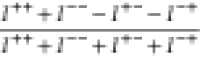 , where IXY represents the intensity of PL with σY-polarization collected under σX-polarized excitation. Figure 3c displays the dependence of ρopt on
magnetic field for iX and 1L-MoSe2 X0. 1L-MoSe2 X0 shows a constant PL polarization degree ∼4%,
consistent with earlier reports.55,56 In contrast,
|ρopt| for iX shows a distinct increase with increasing
|B|, saturating at ∼6% above ±20 mT (see
inset in Figure 3c).
This dependence is consistent across all devices, with |ρopt| ranging from 6% to 14%. In the absence of a magnetic field,
|ρopt| ranges from 0% to 7%. Similar sharp changes
in valley polarization degree with magnetic field have been observed
for iX in 1L-MoSe2/1L-WSe257 and 1L-MoS2/1L-WSe258, as well as intralayer excitons in 1L-WS2 and
1L-WSe2.59 This effect was attributed
to the suppression of intervalley scattering of intralayer excitons
within the monolayer with dark excitonic ground state.6 However, we observe device-specific saturation field for
ρopt (Bsat) ranging from
0.02 to 3 T (Supporting Information Figure S9), indicating that it is not defined by the properties of individual
monolayers, but the collective property of the assembled LMH.
, where IXY represents the intensity of PL with σY-polarization collected under σX-polarized excitation. Figure 3c displays the dependence of ρopt on
magnetic field for iX and 1L-MoSe2 X0. 1L-MoSe2 X0 shows a constant PL polarization degree ∼4%,
consistent with earlier reports.55,56 In contrast,
|ρopt| for iX shows a distinct increase with increasing
|B|, saturating at ∼6% above ±20 mT (see
inset in Figure 3c).
This dependence is consistent across all devices, with |ρopt| ranging from 6% to 14%. In the absence of a magnetic field,
|ρopt| ranges from 0% to 7%. Similar sharp changes
in valley polarization degree with magnetic field have been observed
for iX in 1L-MoSe2/1L-WSe257 and 1L-MoS2/1L-WSe258, as well as intralayer excitons in 1L-WS2 and
1L-WSe2.59 This effect was attributed
to the suppression of intervalley scattering of intralayer excitons
within the monolayer with dark excitonic ground state.6 However, we observe device-specific saturation field for
ρopt (Bsat) ranging from
0.02 to 3 T (Supporting Information Figure S9), indicating that it is not defined by the properties of individual
monolayers, but the collective property of the assembled LMH.
Figure 4a presents the polarization-resolved decay of iX PL recorded at 0 and 40 mT in a device with Bsat ∼ 200 mT. The difference in intensity for cross-co polarization allows us to monitor |ρopt| as a function of time. Figure 4b plots the time-resolved ρopt extracted from the iX PL decay measured at 0 and 40 mT; the solid curves are guides to the eye. Without magnetic field (black filled circles), iX has a low polarization degree (|ρopt| < 2%) throughout the measurement range. In contrast, at B = 40 mT (gray filled circles) |ρopt| starts at 6% and shows a gradual decay toward zero, with a characteristic 1/e time ∼2 μs. These results indicate that the loss of valley polarization for iX is governed by at least two processes occurring at different time scales: 1) fast intervalley relaxation with a characteristic time shorter than 10 ns (i.e., timing resolution of our measurement) dominates at zero magnetic field. 2) This process is suppressed at 40 mT, revealing a slower microsecond-scale relaxation. We note that this time scale directly reflects the loss of valley polarization.
Figure 4.

Temporal evolution of iX valley polarization. (a) Polarization-resolved iX PL decay acquired at 0 and 40 mT using σ+ polarized excitation; blue (red) curve corresponds to PL intensity co- (cross-) polarized with the excitation laser; the data sets are offset for clarity and normalized to the intensity of copolarized component at zero delay. (b) Time-resolved changes of ρopt for B = 0 mT (black) and B = 40 mT (gray). The solid curves are guides to the eye.
In conclusion, we showed that iX in 1L-MoS2/1L-MoSe2 is formed by electrons and holes residing at the edges of the Brillouin zone, with a negligible degree of interlayer hybridization. We find that iX retains its optically induced valley polarization, with the cross-polarized iX PL stemming from the moiré-induced reversal of selection rules. Magnetic field enhances valley-polarization retention by suppressing fast intervalley scattering. The typical magnetic field required for this (≤200 mT) is within reach of a variety of readily accessible techniques, including assembling heterostructures on magnetic substrates60 or using rare-earth magnets.61 In some devices, we observed |ρopt| up to 7% at zero field, allowing for magnet-free operation. The combination of microsecond-long iX PL lifetime and the retention of valley polarization offers the prospect of combining excitonic and valleytronic functionalities in a single optoelectronic device.
Methods
Sample Fabrication
All flakes used for the fabrication of the electrically tunable 1L-MoS2/1L-MoSe2 are produced by micromechanical cleavage of bulk crystals. Bulk TMD crystals are prepared by a flux zone growth method,62 and bulk hBN crystals are grown by the temperature-gradient method.63 Graphite crystals are sourced from NGS. The thickness of exfoliated crystals is estimated using optical contrast64 and confirmed using PL and Raman spectroscopy for TMDs under 532 nm (2.33 eV) laser illumination (LabRAM HR Evolution, Horiba) and atomic force microscopy for hBN (Dimension Icon, Bruker). Electrically tunable heterobilayer devices are assembled by deterministic dry mechanical transfer using polymer stamps.34,35 θ is identified using polarization-resolved SHG65 measured at RT using a custom-built optical setup. The SHG laser is a Chameleon Compact Optical Parametric Oscillator providing ∼200 fs pulses with a repetition rate of 80 MHz centered at 1320 nm. To minimize chromatic aberrations, a linearly polarized laser beam with ∼5 mW power is focused onto the sample using a 40x reflective objective (numerical aperture of 0.5, LMM40X-P01, Thorlabs). Polarization orientation is controlled using a superachromatic half-wave plate (SAHWP05M-1700, Thorlabs) mounted in a motorized rotational mount. Electrical contacts to TMD layers and transparent FLG gates are created by direct laser lithography (LW-405B+, Microtech) with a positive resist (AZ5214E, MicroChemicals) followed by electron beam evaporation (PVD200Pro, Kurt J. Lesker) of 5 nm of Cr followed by 45 nm of Au. The resist excess metal layer is then lifted off by immersion in acetone and isopropanol for 30 min.
Photoluminescence Measurements
RT PL measurements are performed using a LabRAM HR Evolution Raman microscope under 532 nm (2.33 eV) laser illumination. Helicity-resolved magneto-optical measurements are done in a close-cycle bath cryostat (Attodry 1000, Attocube) equipped with a superconducting magnet at a nominal sample temperature of 4 K. Excitation and collection light pass through a home-built confocal microscope in reflection geometry, with a 0.81 numerical aperture apochromatic objective (LT-307 APO/NIR/0.81, Attocube). The PL measurements are taken using 638 nm (1.94 eV) continuous-wave excitation (MCLS1-638, Thorlabs), with incident power below 5 μW. The PL signal collected in epi-direction is isolated using a long-pass filter (FELH0700, Thorlabs) and detected by a 0.75-m spectrometer (SpectraPro 2750, Princeton Instruments) with 150 l mm–1 grating and a nitrogen-cooled CCD camera (Spec-10, Princeton Instruments). Time-resolved measurements are performed using a single-photon avalanche photodiode (SPCM-AQRH-16-FC, Excelitas Technologies) and a time-to-digital converter (quTAU, qutools GmbH) with a 81 ps timing resolution. For these measurements, the intensity of the CW laser is modulated using an acousto-optic modulator (MT350-A0.12-VIS, AA Opto Electronic), producing 200 ns pulses with the 100-kHz repetition rate. A dual-channel source meter (2612B, Keithley) is used for electric field tuning.
Acknowledgments
We acknowledge funding from the EU Graphene and Quantum Flagships, ERC Grants Hetero2D, GSYNCOR, GIPT, EIC Grant CHARM, and EPSRC Grants EP/K01711X/1, EP/K017144/1, EP/N010345/1, EP/L016087/1, EP/X015742/1, EP/V000055/1, The Netherlands Organisation for Scientific Research (NWO 019.221EN.004, Rubicon 2022-1 Science), DOE-SC0020653 (materials synthesis), JSPS KAKENHI (Grant Nos. 21H05233 and 23H02052) and World Premier International Research Center Initiative (WPI), MEXT, Japan. We thank V. Falko, C. Faugeras, and I. Paradisanos for fruitful discussions.
Supporting Information Available
The Supporting Information is available free of charge at https://pubs.acs.org/doi/10.1021/acs.nanolett.4c02635.
Additional data and analysis, including table with the summary of device parameters, Raman spectra, identification of stacking configuration, room-temperature photoluminescence spectra, second harmonic generation plots, atomic force microscopy characterization, Stark tuning for additional devices, summary of photoluminescence lifetimes, g-factors, and magnetic-field dependence of optically induced valley polarization for the six closely aligned devices used in the study (PDF)
The authors declare no competing financial interest.
Supplementary Material
References
- Mak K. F.; Shan J. Photonics and Optoelectronics of 2D Semiconductor Transition Metal Dichalcogenides. Nat. Photonics 2016, 10, 216–226. 10.1038/nphoton.2015.282. [DOI] [Google Scholar]
- Zhou X.; Hu X.; Yu J.; Liu S.; Shu Z.; Zhang Q.; Li H.; Ma Y.; Xu H.; Zhai T. 2D Layered Material-Based Van Der Waals Heterostructures for Optoelectronics. Adv. Funct. Mater. 2018, 28, 1706587. 10.1002/adfm.201706587. [DOI] [Google Scholar]
- Woessner A.; Lundeberg M. B.; Gao Y.; Principi A.; Alonso-González P.; Carrega M.; Watanabe K.; Taniguchi T.; Vignale G.; Polini M.; Hone J.; Hillenbrand R.; Koppens F. H. Highly Confined Low-Loss Plasmons in Graphene-Boron Nitride Heterostructures. Nat. Mater. 2015, 14, 421–425. 10.1038/nmat4169. [DOI] [PubMed] [Google Scholar]
- Ferrari A. C.; et al. Science and Technology Roadmap for Graphene, Related Two-Dimensional Crystals, and Hybrid Systems. Nanoscale 2015, 7, 4598–4810. 10.1039/C4NR01600A. [DOI] [PubMed] [Google Scholar]
- Montblanch A. R.; Barbone M.; Aharonovich I.; Atatüre M.; Ferrari A. C. Layered Materials as a Platform for Quantum Technologies. Nat. Nanotechnol. 2023, 18, 555–571. 10.1038/s41565-023-01354-x. [DOI] [PubMed] [Google Scholar]
- Wang G.; Chernikov A.; Glazov M. M.; Heinz T. F.; Marie X.; Amand T.; Urbaszek B. Colloquium: Excitons in Atomically Thin Transition Metal Dichalcogenides. Rev. Mod. Phys. 2018, 90, 021001. 10.1103/RevModPhys.90.021001. [DOI] [Google Scholar]
- Schaibley J. R.; Yu H.; Clark G.; Rivera P.; Ross J. S.; Seyler K. L.; Yao W.; Xu X. Valleytronics in 2D Materials. Nat. Rev. Mater. 2016, 1, 16055. 10.1038/natrevmats.2016.55. [DOI] [Google Scholar]
- Vitale S. A.; Nezich D.; Varghese J. O.; Kim P.; Gedik N.; Jarillo-Herrero P.; Xiao D.; Rothschild M. Valleytronics: Opportunities, Challenges, and Paths Forward. Small 2018, 14, 1801483. 10.1002/smll.201801483. [DOI] [PubMed] [Google Scholar]
- Novoselov K. S.; Mishchenko A.; Carvalho A.; Castro Neto A. H. 2D Materials and Van Der Waals Heterostructures. Science (80-.) 2016, 353, aac9439. 10.1126/science.aac9439. [DOI] [PubMed] [Google Scholar]
- Liu Y.; Huang Y.; Duan X. Van Der Waals Integration Before and Beyond Two-Dimensional Materials. Nature 2019, 567, 323–333. 10.1038/s41586-019-1013-x. [DOI] [PubMed] [Google Scholar]
- Catanzaro A.; et al. Resonant Band Hybridization in Alloyed Transition Metal Dichalcogenide Heterobilayers. Adv. Mater. 2024, 36, 2309644. 10.1002/adma.202309644. [DOI] [PubMed] [Google Scholar]
- Wilson N. P.; Yao W.; Shan J.; Xu X. Excitons and Emergent Quantum Phenomena in Stacked 2D Semiconductors. Nature 2021, 599, 383–392. 10.1038/s41586-021-03979-1. [DOI] [PubMed] [Google Scholar]
- Ciarrocchi A.; Tagarelli F.; Avsar A.; Kis A. Excitonic Devices With Van Der Waals Heterostructures: Valleytronics Meets Twistronics. Nat. Rev. Mater. 2022, 7, 449–464. 10.1038/s41578-021-00408-7. [DOI] [Google Scholar]
- Mak K. F.; Shan J. Semiconductor Moiré Materials. Nat. Nanotechnol. 2022, 17, 686–695. 10.1038/s41565-022-01165-6. [DOI] [PubMed] [Google Scholar]
- Rivera P.; Yu H.; Seyler K. L.; Wilson N. P.; Yao W.; Xu X. Interlayer Valley Excitons in Heterobilayers of Transition Metal Dichalcogenides. Nat. Nanotechnol. 2018, 13, 1004–1015. 10.1038/s41565-018-0193-0. [DOI] [PubMed] [Google Scholar]
- Regan E. C.; Wang D.; Paik E. Y.; Zeng Y.; Zhang L.; Zhu J.; MacDonald A. H.; Deng H.; Wang F. Emerging Exciton Physics in Transition Metal Dichalcogenide Heterobilayers. Nat. Rev. Mater. 2022, 7, 778–795. 10.1038/s41578-022-00440-1. [DOI] [Google Scholar]
- Montblanch A. R.; et al. Confinement of Long-Lived Interlayer Excitons in WS2/WSe2 Heterostructures. Commun. Phys. 2021, 4, 119. 10.1038/s42005-021-00625-0. [DOI] [Google Scholar]
- Rivera P.; Seyler K. L.; Yu H.; Schaibley J. R.; Yan J.; Mandrus D. G.; Yao W.; Xu X. Valley-Polarized Exciton Dynamics in a 2D Semiconductor Heterostructure. Science (80-.) 2016, 351, 688–691. 10.1126/science.aac7820. [DOI] [PubMed] [Google Scholar]
- Jauregui L. A.; et al. Electrical Control of Interlayer Exciton Dynamics in Atomically Thin Heterostructures. Science (80-.) 2019, 366, 870–875. 10.1126/science.aaw4194. [DOI] [PubMed] [Google Scholar]
- Nayak P. K.; Horbatenko Y.; Ahn S.; Kim G.; Lee J.-U.; Ma K. Y.; Jang A.-R.; Lim H.; Kim D.; Ryu S.; Cheong H.; Park N.; Shin H. S. Probing Evolution of Twist-Angle-Dependent Interlayer Excitons in MoSe2/WSe2 Van Der Waals Heterostructures. ACS Nano 2017, 11, 4041–4050. 10.1021/acsnano.7b00640. [DOI] [PubMed] [Google Scholar]
- Kunstmann J.; Mooshammer F.; Nagler P.; Chaves A.; Stein F.; Paradiso N.; Plechinger G.; Strunk C.; Schüller C.; Seifert G.; Reichman D. R.; Korn T. Momentum-Space Indirect Interlayer Excitons in Transition-Metal Dichalcogenide Van Der Waals Heterostructures. Nat. Phys. 2018, 14, 801–805. 10.1038/s41567-018-0123-y. [DOI] [Google Scholar]
- Alexeev E. M.; et al. Resonantly Hybridized Excitons in Moiré Superlattices in Van Der Waals Heterostructures. Nature 2019, 567, 81–86. 10.1038/s41586-019-0986-9. [DOI] [PubMed] [Google Scholar]
- Kremser M.; Brotons-Gisbert M.; Knörzer J.; Gückelhorn J.; Meyer M.; Barbone M.; Stier A. V.; Gerardot B. D.; Müller K.; Finley J. J. Discrete Interactions Between a Few Interlayer Excitons Trapped at a MoSe2–WSe2 Heterointerface. npj 2D Mater. Appl. 2020, 4, 8. 10.1038/s41699-020-0141-3. [DOI] [Google Scholar]
- Ciarrocchi A.; Unuchek D.; Avsar A.; Watanabe K.; Taniguchi T.; Kis A. Polarization Switching and Electrical Control of Interlayer Excitons in Two-Dimensional Van Der Waals Heterostructures. Nat. Photonics 2019, 13, 131–136. 10.1038/s41566-018-0325-y. [DOI] [PMC free article] [PubMed] [Google Scholar]
- Smirnov D. S.; Holler J.; Kempf M.; Zipfel J.; Nagler P.; Ballottin M. V.; Mitioglu A. A.; Chernikov A.; Christianen P. C. M.; Schüller C.; Korn T. Valley-Magnetophonon Resonance for Interlayer Excitons. 2D Mater. 2022, 9, 045016. 10.1088/2053-1583/ac8602. [DOI] [Google Scholar]
- Gerber I. C.; Courtade E.; Shree S.; Robert C.; Taniguchi T.; Watanabe K.; Balocchi A.; Renucci P.; Lagarde D.; Marie X.; Urbaszek B. Interlayer Excitons in Bilayer MoS2 With Strong Oscillator Strength up to Room Temperature. Phys. Rev. B 2019, 99, 1–8. 10.1103/PhysRevB.99.035443. [DOI] [Google Scholar]
- Barré E.; Karni O.; Liu E.; O’Beirne A. L.; Chen X.; Ribeiro H. B.; Yu L.; Kim B.; Watanabe K.; Taniguchi T.; Barmak K.; Lui C. H.; Refaely-Abramson S.; da Jornada F. H.; Heinz T. F. Optical Absorption of Interlayer Excitons in Transition-Metal Dichalcogenide Heterostructures. Science (80-.) 2022, 376, 406–410. 10.1126/science.abm8511. [DOI] [PubMed] [Google Scholar]
- Seyler K. L.; Rivera P.; Yu H.; Wilson N. P.; Ray E. L.; Mandrus D. G.; Yan J.; Yao W.; Xu X. Signatures of Moiré-Trapped Valley Excitons in MoSe2/WSe2 Heterobilayers. Nature 2019, 567, 66–70. 10.1038/s41586-019-0957-1. [DOI] [PubMed] [Google Scholar]
- Tran K.; et al. Evidence for Moiré Excitons in Van Der Waals Heterostructures. Nature 2019, 567, 71–75. 10.1038/s41586-019-0975-z. [DOI] [PMC free article] [PubMed] [Google Scholar]
- Liu E.; Barré E.; van Baren J.; Wilson M.; Taniguchi T.; Watanabe K.; Cui Y.-t.; Gabor N. M.; Heinz T. F.; Chang Y.-c.; Lui C. H. Signatures of Moiré Trions in WSe2/MoSe2 Heterobilayers. Nature 2021, 594, 46–50. 10.1038/s41586-021-03541-z. [DOI] [PubMed] [Google Scholar]
- Jin C.; Regan E. C.; Wang D.; Iqbal Bakti Utama M.; Yang C.-S.; Cain J.; Qin Y.; Shen Y.; Zheng Z.; Watanabe K.; Taniguchi T.; Tongay S.; Zettl A.; Wang F. Identification of Spin, Valley and Moiré Quasi-Angular Momentum of Interlayer Excitons. Nat. Phys. 2019, 15, 1140–1144. 10.1038/s41567-019-0631-4. [DOI] [Google Scholar]
- Stansbury C. H.; et al. Visualizing Electron Localization of WS 2/WSe 2 Moiré Superlattices in Momentum Space. Sci. Adv. 2021, 7, 1–9. 10.1126/sciadv.abf4387. [DOI] [PMC free article] [PubMed] [Google Scholar]
- Tang Y.; Gu J.; Liu S.; Watanabe K.; Taniguchi T.; Hone J.; Mak K. F.; Shan J. Tuning Layer-Hybridized Moiré Excitons by the Quantum-Confined Stark Effect. Nat. Nanotechnol. 2021, 16, 52–57. 10.1038/s41565-020-00783-2. [DOI] [PubMed] [Google Scholar]
- Castellanos-Gomez A.; Buscema M.; Molenaar R.; Singh V.; Janssen L.; van der Zant H. S. J.; Steele G. a. Deterministic Transfer of Two-Dimensional Materials by All-Dry Viscoelastic Stamping. 2D Mater. 2014, 1, 011002. 10.1088/2053-1583/1/1/011002. [DOI] [Google Scholar]
- Zomer P. J.; Guimarães M. H. D.; Brant J. C.; Tombros N.; van Wees B. J. Fast Pick up Technique for High Quality Heterostructures of Bilayer Graphene and Hexagonal Boron Nitride. Appl. Phys. Lett. 2014, 105, 013101 10.1063/1.4886096. [DOI] [Google Scholar]
- Cadore A. R.; et al. Monolayer WS 2 Electro- and Photo-Luminescence Enhancement by TFSI Treatment. 2D Mater. 2024, 11, 025017. 10.1088/2053-1583/ad1a6a. [DOI] [Google Scholar]
- Gong C.; Zhang H.; Wang W.; Colombo L.; Wallace R. M.; Cho K. Band alignment of two-dimensional transition metal dichalcogenides: Application in tunnel field effect transistors. Appl. Phys. Lett. 2013, 103, 053513. 10.1063/1.4817409. [DOI] [Google Scholar]
- Kang J.; Tongay S.; Zhou J.; Li J.; Wu J. Band offsets and heterostructures of two-dimensional semiconductors. Appl. Phys. Lett. 2013, 102, 012111. 10.1063/1.4774090. [DOI] [Google Scholar]
- Cadiz F.; et al. Excitonic Linewidth Approaching the Homogeneous Limit in MoS2 -Based Van Der Waals Heterostructures. Phys. Rev. X 2017, 7, 021026. 10.1103/PhysRevX.7.021026. [DOI] [Google Scholar]
- Shree S.; Paradisanos I.; Marie X.; Robert C.; Urbaszek B. Guide to Optical Spectroscopy of Layered Semiconductors. Nat. Rev. Phys. 2021, 3, 39–54. 10.1038/s42254-020-00259-1. [DOI] [Google Scholar]
- Lin B.-H.; Chao Y.-C.; Hsieh I.; Chuu C.-P.; Lee C.-J.; Chu F.-H.; Lu L.-S.; Hsu W.-t.; Pao C.-w.; Shih C.-k.; Su J.-j.; Chang W.-h. Remarkably Deep Moiré Potential for Intralayer Excitons in MoSe 2/MoS 2 Twisted Heterobilayers. Nano Lett. 2023, 23, 1306–1312. 10.1021/acs.nanolett.2c04524. [DOI] [PubMed] [Google Scholar]
- Zhu Z. Y.; Cheng Y. C.; Schwingenschlögl U. Giant Spin-Orbit-Induced Spin Splitting in Two-Dimensional Transition-Metal Dichalcogenide Semiconductors. Phys. Rev. B 2011, 84, 153402. 10.1103/PhysRevB.84.153402. [DOI] [Google Scholar]
- Constantinescu G. C.; Hine N. D. Energy Landscape and Band-Structure Tuning in Realistic MoS2/MoSe2 Heterostructures. Phys. Rev. B - Condens. Matter Mater. Phys. 2015, 91, 1–8. 10.1103/PhysRevB.91.195416. [DOI] [Google Scholar]
- Liu K.; Zhang L.; Cao T.; Jin C.; Qiu D.; Zhou Q.; Zettl A.; Yang P.; Louie S. G.; Wang F. Evolution of Interlayer Coupling in Twisted Molybdenum Disulfide Bilayers. Nat. Commun. 2014, 5, 4966. 10.1038/ncomms5966. [DOI] [PubMed] [Google Scholar]
- Tebyetekerwa M.; Zhang J.; Saji S. E.; Wibowo A. A.; Rahman S.; Truong T. N.; Lu Y.; Yin Z.; Macdonald D.; Nguyen H. T. Twist-Driven Wide Freedom of Indirect Interlayer Exciton Emission in MoS2/WS2 Heterobilayers. Cell Reports Phys. Sci. 2021, 2, 100509. 10.1016/j.xcrp.2021.100509. [DOI] [Google Scholar]
- Lian Z.; et al. Valley-polarized excitonic Mott insulator in WS2/WSe2 moiré superlattice. Nat. Phys. 2024, 20, 34. 10.1038/s41567-023-02266-2. [DOI] [Google Scholar]
- Wang X.; Zhang X.; Zhu J.; Park H.; Wang Y.; Wang C.; Holtzmann W. G.; Taniguchi T.; Watanabe K.; Yan J.; Gamelin D. R.; Yao W.; Xiao D.; Cao T.; Xu X. Intercell moiré exciton complexes in electron lattices. Nat. Mater. 2023, 22, 599. 10.1038/s41563-023-01496-2. [DOI] [PubMed] [Google Scholar]
- He J.; Hummer K.; Franchini C. Stacking Effects on the Electronic and Optical Properties of Bilayer Transition Metal Dichalcogenides MoS2, MoSe2, WS2, and WSe2. Phys. Rev. B 2014, 89, 075409. 10.1103/PhysRevB.89.075409. [DOI] [Google Scholar]
- Sung J.; et al. Broken Mirror Symmetry in Excitonic Response of Reconstructed Domains in Twisted MoSe2/MoSe2 Bilayers. Nat. Nanotechnol. 2020, 15, 7–12. 10.1038/s41565-020-0728-z. [DOI] [PubMed] [Google Scholar]
- Nagler P.; Ballottin M. V.; Mitioglu A. A.; Mooshammer F.; Paradiso N.; Strunk C.; Huber R.; Chernikov A.; Christianen P. C. M.; Schüller C.; Korn T. Giant Magnetic Splitting Inducing Near-Unity Valley Polarization in Van Der Waals Heterostructures. Nat. Commun. 2017, 8, 1–6. 10.1038/s41467-017-01748-1. [DOI] [PMC free article] [PubMed] [Google Scholar]
- Wozniak T.; Faria Junior P. E.; Seifert G.; Chaves A.; Kunstmann J. Exciton G-Factors of Van Der Waals Heterostructures From First Principles Calculations. Phys. Rev. B 2020, 101, 1–27. 10.1103/PhysRevB.101.235408. [DOI] [Google Scholar]
- Li Y.; Ludwig J.; Low T.; Chernikov A.; Cui X.; Arefe G.; Kim Y. D.; Van Der Zande A. M.; Rigosi A.; Hill H. M.; Kim S. H.; Hone J.; Li Z.; Smirnov D.; Heinz T. F. Valley Splitting and Polarization by the Zeeman Effect in Monolayer MoSe2. Phys. Rev. Lett. 2014, 113, 1–5. 10.1103/PhysRevLett.113.266804. [DOI] [PubMed] [Google Scholar]
- Koperski M.; Molas M. R.; Arora A.; Nogajewski K.; Bartos M.; Wyzula J.; Vaclavkova D.; Kossacki P.; Potemski M. Orbital, Spin and Valley Contributions to Zeeman Splitting of Excitonic Resonances in MoSe2, WSe2 and WS2Monolayers. 2D Mater. 2019, 6, 015001 10.1088/2053-1583/aae14b. [DOI] [Google Scholar]
- Mak K. F.; He K.; Shan J.; Heinz T. F. Control of Valley Polarization in Monolayer MoS2 by Optical Helicity. Nat. Nanotechnol. 2012, 7, 494–498. 10.1038/nnano.2012.96. [DOI] [PubMed] [Google Scholar]
- Wang G.; Palleau E.; Amand T.; Tongay S.; Marie X.; Urbaszek B. Polarization and Time-Resolved Photoluminescence Spectroscopy of Excitons in MoSe2 Monolayers. Appl. Phys. Lett. 2015, 106, 2–6. 10.1063/1.4916089. [DOI] [Google Scholar]
- MacNeill D.; Heikes C.; Mak K. F.; Anderson Z.; Kormányos A.; Zólyomi V.; Park J.; Ralph D. C. Breaking of Valley Degeneracy by Magnetic Field in Monolayer MoSe2. Phys. Rev. Lett. 2015, 114, 037401. 10.1103/PhysRevLett.114.037401. [DOI] [PubMed] [Google Scholar]
- Jiang C.; Xu W.; Rasmita A.; Huang Z.; Li K.; Xiong Q.; Gao W. B. Microsecond Dark-Exciton Valley Polarization Memory in Two-Dimensional Heterostructures. Nat. Commun. 2018, 9, 753. 10.1038/s41467-018-03174-3. [DOI] [PMC free article] [PubMed] [Google Scholar]
- Tan Q.; Rasmita A.; Li S.; Liu S.; Huang Z.; Xiong Q.; Yang S. A.; Novoselov K. S.; Gao W.-b. B. Layer-Engineered Interlayer Excitons. Sci. Adv. 2021, 7, 1–9. 10.1126/sciadv.abh0863. [DOI] [PMC free article] [PubMed] [Google Scholar]
- Smoleński T.; Kazimierczuk T.; Goryca M.; Molas M. R.; Nogajewski K.; Faugeras C.; Potemski M.; Kossacki P. Magnetic Field Induced Polarization Enhancement in Monolayers of Tungsten Dichalcogenides: Effects of Temperature. 2D Mater. 2018, 5, 015023. 10.1088/2053-1583/aa9811. [DOI] [Google Scholar]
- Gibertini M.; Koperski M.; Morpurgo A. F.; Novoselov K. S. Magnetic 2D Materials and Heterostructures. Nat. Nanotechnol. 2019, 14, 408–419. 10.1038/s41565-019-0438-6. [DOI] [PubMed] [Google Scholar]
- Stern H. L.; Gu Q.; Jarman J.; Eizagirre Barker S.; Mendelson N.; Chugh D.; Schott S.; Tan H. H.; Sirringhaus H.; Aharonovich I.; Atatüre M. Room-Temperature Optically Detected Magnetic Resonance of Single Defects in Hexagonal Boron Nitride. Nat. Commun. 2022, 13, 1–9. 10.1038/s41467-022-28169-z. [DOI] [PMC free article] [PubMed] [Google Scholar]
- Edelberg D.; et al. Approaching the Intrinsic Limit in Transition Metal Diselenides Via Point Defect Control. Nano Lett. 2019, 19, 4371–4379. 10.1021/acs.nanolett.9b00985. [DOI] [PubMed] [Google Scholar]
- Watanabe K.; Taniguchi T.; Kanda H. Direct-Bandgap Properties and Evidence for Ultraviolet Lasing of Hexagonal Boron Nitride Single Crystal. Nat. Mater. 2004, 3, 404–409. 10.1038/nmat1134. [DOI] [PubMed] [Google Scholar]
- Li H.; Wu J.; Huang X.; Lu G.; Yang J.; Lu X.; Xiong Q.; Zhang H. Rapid and Reliable Thickness Identification of Two-Dimensional Nanosheets Using Optical Microscopy. ACS Nano 2013, 7, 10344–10353. 10.1021/nn4047474. [DOI] [PubMed] [Google Scholar]
- Hsu W. T.; Zhao Z. A.; Li L. J.; Chen C. H.; Chiu M. H.; Chang P. S.; Chou Y. C.; Chang W. H. Second Harmonic Generation From Artificially Stacked Transition Metal Dichalcogenide Twisted Bilayers. ACS Nano 2014, 8, 2951–2958. 10.1021/nn500228r. [DOI] [PubMed] [Google Scholar]
Associated Data
This section collects any data citations, data availability statements, or supplementary materials included in this article.