

Abstract
Transition metal dichalcogenide heterostructures have garnered strong interest for their robust excitonic properties, mixed light–matter states such as exciton-polaritons, and tailored properties, vital for advanced device engineering. Two-dimensional heterostructures inherit their physics from monolayers with the addition of interlayer processes that have been particularly emphasized for their electronic and optical properties. Here, we demonstrate the interlayer coupling of the MoSe2 phonons to WSe2 excitons in a WSe2/MoSe2 heterostructure using resonant Raman scattering. The WSe2 monolayer induces an interlayer resonance in the Raman cross-section of the MoSe2 A1g phonons. Frozen-phonon calculations within density functional theory reveal a strong deformation-potential coupling between the A1g MoSe2 phonon and the electronic states of the close-by WSe2 layer approaching 20% of the intralayer coupling to the MoSe2 electrons. Understanding the vibrational properties of van der Waals heterostructures requires going beyond the sum of their constituents and considering cross-material coupling.
Keywords: exciton−phonon, Raman, TMDC, DFT, heterostructures
Van der Waals heterostructures combine monolayer two-dimensional materials into stacks with atomic precision, which achieves an intimate connection of widely different materials.1 In such stacks, transitional metal dichalcogenides (TMDCs) are of particular interest due to their optical properties originating from excitons with large binding energies having potential applications in valleytronics and as hybridized light–matter states.2−6 While van-der-Waals heterostructures were first seen as mere combinations of disparate materials, researchers soon realized that their most intriguing properties arise from a coupling of quasiparticles in different layers. This interlayer interaction induce, e.g., superconductivity in twisted graphene bilayers and interlayer excitons from charge carriers situated in distinct layers.7,8
In contrast to optical and electronic properties, the vibrational response of heterostructures (with the exception of interlayer shear and breathing modes9) has been mainly perceived as the sum of the heterostructure components. Unravelling interlayer vibrational interaction is particularly important when considering that phonons provide the prime relaxation channels for excited charge carriers, are involved in heat transport, and determine exciton dynamics.10,11 A first indication for nontrivial effects of van der Waals stacking on phonons was the appearance of silent h-BN phonons in the Raman spectrum of a WSe2/h-BN heterostructure. It was attributed to an interaction of the h-BN phonons with a new optical transition of the heterostructure.12 Other indications of interlayer exciton–phonon coupling were twist-induced scattering for the double-resonant Raman process of graphene as well as a preserved photohelicity in the emission from an h-BN/WSe2/h-BN heterostructure.13,14 Reports of interlayer vibrational coupling to date have focused on the activation of new Raman modes by breaking the point and translational symmetries. No study has followed exciton–phonon coupling in TMD heterostructures across their excitonic resonance to observe the coupling between Raman-allowed phonons and the optical excitations of such devices. We need to unravel the vibrational dimension of the interlayer interaction to fully understand and engineer the heterostructure response.
In this paper, we directly observe interlayer exciton–phonon coupling in a WSe2/MoSe2 heterostructure using multiwavelength Raman scattering in resonance with the A excitons of the two materials (1.5–1.8 eV). We observe a WSe2-related Raman resonance for the A1g mode of MoSe2, meaning that the A1g phonon of MoSe2 scatters with the A exciton in the WSe2 layer (interlayer) in addition to its scattering with the A exciton of MoSe2 (intralayer). In contrast, no interlayer resonance is observed for the WSe2 A1g phonon. The inter- and intralayer resonances of the A1g phonons are explained by the strength of light–matter interaction and exciton–phonon coupling in the two materials, as we show by ab initio calculations of the phonon-deformation potential. The intralayer interactions open additional relaxation channels for excited carriers in TMD heterostructures compared to the pristine material. Our findings also imply that Raman characterization of van der Waals materials needs to consider interlayer coupling.
We first discuss the electronic states and optical transitions of the MoSe2/WSe2 heterostructure. In an MoSe2/WSe2 heterostructure with strong layer interaction, the electronic band configuration is a type II staggered alignment, meaning the conduction band minimum is localized in the MoSe2 layer while the valence band maximum is localized in the WSe2 layer as illustrated in Figure 1.15,16 The blue label XAM indicates the transitions that lead to the A exciton at the K point for MoSe2 and the red label XAW for WSe2 monolayers. These momentum-direct excitons have a transition energy of 1.59 eV in MoSe2 (blue) and 1.66 eV in WSe2 (red) for the monolayer case, and 1.57 eV in MoSe2 and 1.64 eV in WSe2 for the heterostructure case (black), see PL in Figure 2b.15 The label XI denotes interlayer excitons formed by combining the electronic states of MoSe2 and WSe2.17
Figure 1.
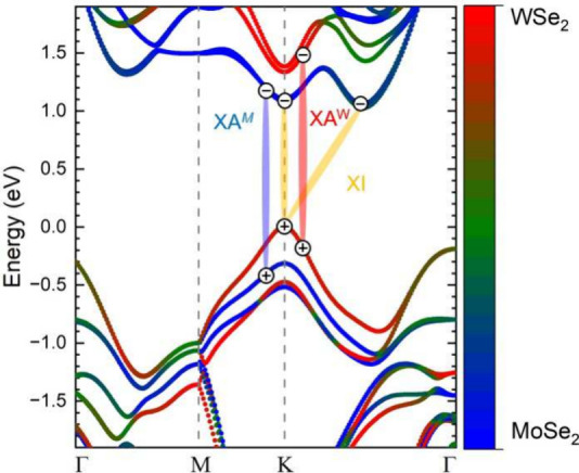
Electronic dispersion of the MoSe2/WSe2 heterostructure showing a staggered band alignment. The color scale indicates in which layer the bands are localized, blue for MoSe2, red for WSe2, and green for an equal band contribution from both layers. The blue label XAM refers to the A-excitonic transition in MoSe2, while the red label XAW is the A-excitonic transition in WSe2. The interlayer transition, labeled XI, originates from combining MoSe2 and WSe2 states into an exciton.
Figure 2.

(a) Sketch of an MoSe2/WSe2 heterostructure on a SiO2. Featured are an intralayer exciton (left) with electron and hole within one layer and an interlayer exciton (right) where the bound electron and hole are localized in different layers. (b) Room-temperature PL spectra of monolayer MoSe2 (blue, scaled down), monolayer WSe2 (red, scaled down), and the heterostructure (black) from intralayer A-exciton transitions of 1.57 eV (MoSe2) and 1.64 eV (WSe2) and the interlayer exciton transition of 1.34 eV. (c) PL intensity map taken at 1.35 eV at room temperature.
When the layers are decoupled or interact only weakly, the heterostructure emits light from the intralayer XA excitons, Figure 2a, of both layers, as seen at 1.57 eV (MoSe2) and 1.66 eV (WSe2) in the spectrum in Figure 2b. For strongly interacting layers, some charge carriers participate in the interlayer XI exciton emission at 1.35 eV, lowering the intensity of the XA excitons, black line in Figure 2b.15,17,18 The peak energy and relative intensities of the interlayer PL in our device suggest an H-type stacking of the two layers, i.e., a twist angle of ∼60°.19 A map of the interlayer PL intensity in Figure 2c shows areas of strong interaction (red), individual WSe2 monolayer (green), and the SiO2 substrate (blue); this was used to identify individual layers and strongly coupled areas of the MoSe2/WSe2 heterostructures for the Raman experiments.
Figure 3 shows Raman spectra taken with tunable laser excitations in the spectral region of the XA excitons of (a) a MoSe2 monolayer with the out-of-plane phonon mode AM1g at 242 cm–1 (blue arrow) and (b) a WSe2 monolayer with the out-of-plane phonon mode AW1g at 250 cm–1 (red arrow) and the peak by the overtone of the longitudinal acoustic phonon 2LA at 261 cm–1 (gray arrow).20−22 These three Raman peaks also appear in the MoSe2/WSe2 heterostructure, Figure 3c, but for a given wavelength with somewhat altered intensities compared to those in the monolayer case. This change in the relative scattering intensities is caused by changes in the electronic structure and electron–phonon coupling due to the stacking.23 The quantum theory of the Raman effect describes it as a three-step process of (i) absorption of an incoming photon and creation of an electron–hole pair, (ii) scattering of the carriers under phonon emission via electron–phonon scattering, and (iii) recombination of the electron–hole pair at different energies. The energy difference between the incoming and scattered light is given by the phonon energy, but the scattering intensity is given by light–matter (steps i and iii) and electron–phonon coupling, (step ii). When varying the laser energy, Figure 3, the scattering intensities of the AM1g mode (blue arrow) and the AW1g mode (red arrow) vary compared to the constant scattering by Si.24 The integrated intensity of a Raman peak greatly increases when the laser energy matches a real electronic transition in a material such as the XA excitons. This reflects the increasing probability for photon absorption and emission (steps i and iii) and allows the study of electronic transitions and their coupling to phonons through the Raman effect. No Raman peaks were observed from the heterostructure, with laser energies at the XI exciton (1.35 eV). The XI transition induced no resonance in the Raman cross sections because it originates from an indirect excitation via XA states.
Figure 3.
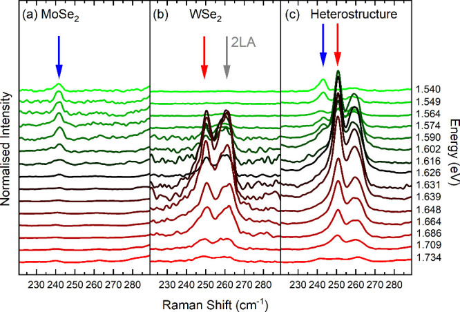
Raman spectra excited with tunable laser wavelength/energy at 1.5–1.8 eV (see labels) of the (a) MoSe2 mode AM1g at 242 cm–1 (blue arrow), (b) WSe2 mode AW1g at 250 cm–1 (red arrow) and 2LA mode at 261 cm–1 (gray), and (c) heterostructure A1g modes from MoSe2 (blue arrow) and WSe2 (red arrow). All spectra measured at room temperature under ambient conditions and normalized to the Si scattering intensity.
To quantitatively analyze the A1g resonances, we determined the integrated intensity peaks in Figure 3a–c by fitting the spectra and extracting the area under the curve, see the Supporting Information. From the fits, we prepared a resonance Raman profile, shown in Figure 4, i.e., a plot of the integrated peak intensity as a function of excitation energy. The resonance profile is described within the quantum theory of Raman scattering discussed above using third-order perturbation theory,23,25
| 1 |
In this expression, Mi is the electron-photon matrix element of the electronic transition i and Mep,i the electron–phonon matrix element of the excited charge carrier. El is the excitation laser energy. ωph is the phonon frequency, and γi is the decay rate of the excited electronic state. We simplified the most general expression for the Raman cross section by introducing distinct intermediate excitonic states Ei (i represents the XA exciton of MoSe2 or WSe2).25 When the laser energy approaches a material transition energy, El ≈ Ei in eq 1 and the real part of the denominator vanishes, giving rise to a Raman resonance. Note that each transition induces two resonances, an incoming resonance if the laser matches an electronic transition and an outgoing resonance if the scattered photon matches the transition energy. The electron–photon and electron–phonon matrix elements in eq 1 are considered to be constant and are typically treated as one fitting parameter in the analysis of resonance profiles. The measured Raman profiles we fit with IR, full lines in Figure 4; the parameters are given in Table 1.
Figure 4.
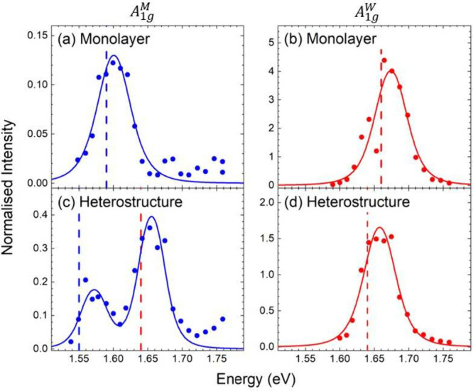
Resonant Raman profiles of the heterostructure and their monolayers. Data points are room-temperature integrated peak intensities normalized to Si of the (a) AM1g monolayer, (b) AW1g monolayer, (c) AM1g heterostructure, and (d) AW1g heterostructure profiles. Full lines are fits with eq 1, see Table 1 and Supporting Information. Dashed lines mark the fitted energies of the XA excitons originting from the blue MoSe2 and red WSe2 layer.
Table 1. Fits of the Raman Resonance Profiles with eq 1 Giving the A1g Frequency, the XA Resonance Energy, and the Decay Rate γa.
| monolayer |
heterostructure |
||||
|---|---|---|---|---|---|
| A1g (cm–1) | XA (eV) | γr (eV) | XA (eV) | γr (eV) | |
| MoSe2 | 242 | 1.59 | 0.08 | 1.55 | 0.05 |
| 1.64 | 0.05 | ||||
| WSe2 | 250 | 1.66 | 0.06 | 1.64 | 0.06 |
The MoSe2 of the heterostructure shows a second resonance at the energy of the XAW exciton.
The A1g Raman profiles show resonances from intralayer coupling to the XA excitons of the monolayers or heterostructure components, as shown in Figure 4. These resonances shift by up to 40 meV to smaller energies in the MoSe2/WSe2 heterostructure, Table 1. Similar shifts have been noted before in TMD heterostructures and attributed to strain, doping, and the change in dielectric environment due to the second layer.26−28 The most intriguing feature in the resonance profiles of the MoSe2/WSe2 heterostructure, however, is the additional second resonance of the MoSe2 derived AM1g phonon at the XA exciton energy of WSe2. This manifests an interlayer exciton–phonon coupling in the heterostructure. The interlayer resonance is stronger in intensity than the intralayer resonance, which appears counterintuitive and requires further examination.
When the three steps in the Raman process are considered, only electron–phonon coupling can give rise to an interlayer Raman resonance. A photon that matches the XAM cannot create an exciton in the WSe2 component at energy XAW and vice versa, ruling out an exciton-induced interlayer coupling. On the other hand, there are two mechanisms for the interlayer interaction in the phonon part of the Raman process: The phonons of the monolayer may mix in the heterostructure, so that a predominantly AM1g phonon of MoSe2 also leads to vibrations in the WSe2 layer. Alternatively, the electron wave functions of one monolayer may extend into the other layer and get affected by the vibration of the nearby atoms. To understand the interlayer electron–phonon coupling in the MoSe2/WSe2 heterostructure, we calculated the phonon frequencies and eigenvectors as well as their electron–phonon coupling using density functional theory.
Indeed, the eigenvectors of the heterostructure mix between the two layers, as shown in Figure 5a. The AM1g mode of the heterostructure that is predominantly an out-of-plane vibration of the MoSe2 selenide atoms, also involves a movement of the WSe2 atoms and vice versa. In addition, the symmetry breaking by the heterostructure induces movement of both chalcogen atoms vibrating against each other. The eigenfrequencies of the heterostructure are 1 cm–1 higher than in the monolayer. The mixing of the eigenvectors results in an induced movement in the adjacent layer that is as strong as 17% of the source layers movement, see Supporting Information Table 2.
Figure 5.

(a) Eigenvectors and frequencies of the A1g modes for the monolayers (left) and the heterostructure (right). The displacement vectors of the induced vibrations are magnified for clarity; for the unaltered vectors, see Supporting Information Table 2. (b–d) Change of the electronic states in the heterostructure under an atomic displacement according to the eigenvectors in the inset. Red lines are for positive, black lines for negative displacement, and dashed lines for the equilibrium atomic positions. (b) Eigenvector AM1g in a and c monolayer eigenvector with the WSe2 atoms fixed at equilibrium position; c and d are the corresponding plots for the AW1g mode.
The deformation potential simulation finds both intra- and interlayer electron–phonon coupling for the A1g modes of the heterostructure. The intralayer deformation potentials for H-type stacking is 104 eV/Å for AM1g/XAM coupling—the intralayer coupling of the MoSe2AM1g mode to the MoSe2 electrons—and 194 eV/Å for AW1g/XAW coupling. This is comparable to electron–phonon coupling in graphene29 but larger than in classical semiconductors such as GaAs.30 The calculations predict the interlayer coupling of the AM1g mode to the XAW exciton AM1g/XAW (22 eV/Å) to be 20% of the intralayer coupling. The absolute numbers in Table 2 differ somewhat for R-type stacking, but overall, our calculations find interlayer electron–phonon interaction in the MoSe2/WSe2 heterostructure, in excellent agreement with experimental results.
Table 2. Deformation Potentials for the AM1g and AW1g Heterostructure Eigenvectors on the MoSe2 and WSe2 Bands at K (○ = M, W)a.
| MA1gM/XA° (eV/Å) | MA1gW/XA° (eV/Å) | ratio | |
|---|---|---|---|
| H-type stacking | |||
| MA1g°/XAM | 104 | 22 | 0.21 |
| MA1g°/XAW | 4 | 194 | 0.02 |
| R-type stacking | |||
| MA1g°/XAM | 160 | 28 | 0.18 |
| MA1g°/XAW | 17 | 199 | 0.09 |
The other heterostructure stackings are reported in Supporting Information Table I.
To quantify if the larger contribution to the interlayer coupling is from the mixing of phonon eigenmodes, Figure 5a, or from the wave function overlap with the adjacent layer, we repeated the deformation potential calculations using the monolayer phonon eigenvector for one layer keeping the other layer fixed in position. The resulting bandstructures around K differ little between the simulations of the hybridized, Figure 5b and d, and the monolayer eigenvectors, Figure 5c and e. The major contributor to the interlayer electron–phonon coupling arises from the electronic states of the intralayer exciton overlapping with the adjacent layer so that the moving MoSe2 atoms affect the eigenenergies of the WSe2 electronic states. The mixing of the eigenvectors is of minor importance to interlayer coupling.
We now return to the surprisingly intense interlayer resonance of the AM1g mode, Figure 4c. It originates from the strong absorption of XAW compared to XAM that counteracts the weaker interlayer coupling compared to that of the intralayer interaction. To show this, we consider the expression for the resonant Raman intensity eq 1 and approximate the transitions to intermediate excitonic states by the absorption coefficient α.25 Making use of ℏωph ≪ El for eq 1, we obtain
| 2 |
The absorption coefficient for MoSe2 in the investigated spectral range is αM ≈ 104 cm–1 in contrast to αW ≈ 105 cm–1 for WSe2.31,32 The different exciton transition probabilities are also apparent from the monolayer PL intensities (see Supporting Information Figure 3), with an intensity ratio between the WSe2 and MoSe2:
| 3 |
To calculate the ratio between the interlayer and the intralayer scattering of AM1g mode, we use the deformation potentials in Table 2 and obtain
| 4 |
Given the uncertainties in our estimates, this is in reasonably good agreement with the similar intensity of the interlayer (AM1g/XAW) and intralayer (AM1g/XAM) resonances in Figure 4c. For the AW1g mode, in contrast, the ratio between the absorption coefficient is inverse, and the interlayer electron–phonon coupling is less than 10% of the intralayer coupling. This leads to an expected intensity ratio of 10–5 between the inter- and intralayer WSe2 phonon resonances. The interlayer AW1g resonance is too weak to be detected in the heterostructure, in agreement with our experimental findings. Equation 2 also explains the different Raman intensities observed between the two monolayers. The intralayer coupling and the absorption coefficient are larger in the WSe2 than in the MoSe2 layer, yielding an estimated intensity ratio of 50 based on eq 2 compared to an experimental ratio of 30, Figure 4a and b.
In summary, we studied interlayer and intralayer exciton–phonon coupling in a MoSe2/WSe2 heterostructure using resonant Raman scattering and ab initio calculations. We find that excitons in the heterostructure interact with phonons in adjacent layers via the deformation potential mechanism. Experimentally, we observed that the intensity of the interlayer Raman resonance for the A1g phonon of MoSe2 is comparable to that of the intralayer resonance within the material. This originates from the absorption coefficient of WSe2 and the relatively strong interlayer coupling of the MoSe2 phonon. We show, using density functional analysis, that the largest contribution to this interlayer exciton–phonon coupling is from the overlapping of the electronic states of the XAW intralayer exciton with the MoSe2 layer, rather than the mixing of the A1g phonon eigenvectors. In contrast, only intralayer resonances were observed in WSe2 due to the small interlayer exciton–phonon coupling of this mode and the weaker absorption in MoSe2. Understanding the vibrational properties of TMD heterostructures as well as their carrier relaxation requires the consideration of interlayer interactions beyond the emergence of interlayer excitons. The interlayer vibrational coupling will be beneficial for further device engineering. One could selectively create a resonance in a TMDC monolayer with the appropriate choice of crystal, with tailored electronic and vibrational properties, and with the appropriate phonon mode symmetry.
Acknowledgments
This work was supported by the German Science Foundation (DFG) under the priority program SPP2244 (projects 443361515 and 443275027). P.K. and O.G. acknowledge the DFG project KU4034/2-1 for funding. Computing time was made available on the high-performance computer at the NHR Centre of TU Dresden funded by the German Federal Ministry of Education and Research and the state governments participating on the basis of the resolutions of the GWK for the national high-performance computing at universities (www.nhr-verein.de/unsere-partner). Parts of this work were supported by the European Research Council (ERC) DarkSERS (project 772108) and the DFG (project 440298568). T.B. acknowledges the DFG for SFB 1415 (project 417590517), SFB1477 (project 441234705), and KO3612/7-1. This work was supported by the SupraFAB Research Facility and the Focus Area NanoScale at Freie Universität Berlin.
Supporting Information Available
The Supporting Information is available free of charge at https://pubs.acs.org/doi/10.1021/acs.nanolett.4c02757.
Experimental details and sample production as well as a description of the fitting procedure using eq 1 to fit the Raman spectra shown in Figure 3; additional figures showing the sample area, PL spectra from the monolayers, and a table of optical deformation potentials as well as how they were calculated (PDF)
The authors declare no competing financial interest.
Supplementary Material
References
- Geim A. K.; Grigorieva I. V. Van der Waals heterostructures. Nature 2013, 499, 419. 10.1038/nature12385. [DOI] [PubMed] [Google Scholar]
- Xiao J.; Zhao M.; Wang Y.; Zhang X. Excitons in atomically thin 2D semiconductors and their applications. Nanophotonics 2017, 6, 1309. 10.1515/nanoph-2016-0160. [DOI] [Google Scholar]
- Li M. Y.; Chen C. H.; Shi Y.; Li L. J. Heterostructures based on two-dimensional layered materials and their potential applications. Mater. Today 2016, 19, 322. 10.1016/j.mattod.2015.11.003. [DOI] [Google Scholar]
- Liu Y.; Weiss N. O.; Duan X.; Cheng H.-C.; Huang Y.; Duan X. Van der Waals heterostructures and devices. Nat. Rev. Mater. 2016, 1, 16042. 10.1038/natrevmats.2016.42. [DOI] [Google Scholar]
- Shanmugam M.; Jacobs-Gedrim R.; Song E. S.; Yu B. Two-dimensional layered semiconductor/graphene heterostructures for solar photovoltaic applications. Nanoscale 2014, 6, 12682. 10.1039/C4NR03334E. [DOI] [PubMed] [Google Scholar]
- Furchi M. M.; Pospischil A.; Libisch F.; Burgdörfer J.; Mueller T. Photovoltaic Effect in an Electrically Tunable van der Waals Heterojunction. Nano Lett. 2014, 14, 4785. 10.1021/nl501962c. [DOI] [PMC free article] [PubMed] [Google Scholar]
- Yankowitz M.; Chen S.; Polshyn H.; Zhang Y.; Watanabe K.; Taniguchi T.; Graf D.; Young A. F.; Dean C. R. Tuning superconductivity in twisted bilayer graphene. Science 2019, 363, 1059. 10.1126/science.aav1910. [DOI] [PubMed] [Google Scholar]
- Ovesen S.; Brem S.; Linderälv C.; Kuisma M.; Korn T.; Erhart P.; Selig M.; Malic E. Interlayer exciton dynamics in van der Waals heterostructures. Commun. Phys. 2019, 2, 23. 10.1038/s42005-019-0122-z. [DOI] [Google Scholar]
- Pizzi G.; Milana S.; Ferrari A. C.; Marzari N.; Gibertini M. Shear and Breathing Modes of Layered Materials. ACS Nano 2021, 15, 12509. 10.1021/acsnano.0c10672. [DOI] [PMC free article] [PubMed] [Google Scholar]
- Tornatzky H.Phononic and Excitonic Properties of Transition Metal Dichalcogenides; Ph.D. thesis; Technische Universität: Berlin, 2019; 10.14279/depositonce-9069. [DOI] [Google Scholar]
- Rosser D.; Fryett T.; Ryou A.; Saxena A.; Majumdar A. Exciton–phonon interactions in nanocavity-integrated monolayer transition metal dichalcogenides. npj 2D Mater. Appl. 2020, 4, 20. 10.1038/s41699-020-0156-9. [DOI] [Google Scholar]
- Jin C.; Kim J.; Suh J.; Shi Z.; Chen B.; Fan X.; Kam M.; Watanabe K.; Taniguchi T.; Tongay S.; Zettl A.; Wu J.; Wang F. Interlayer electron-phonon coupling in WSe 2/hBN heterostructures. Nat. Phys. 2017, 13, 127. 10.1038/nphys3928. [DOI] [Google Scholar]
- Eliel G. S. N.; Moutinho M. V. O.; Gadelha A. C.; Righi A.; Campos L. C.; Ribeiro H. B.; Chiu P.-W.; Watanabe K.; Taniguchi T.; Puech P.; Paillet M.; Michel T.; Venezuela P.; Pimenta M. A. Intralayer and interlayer electron–phonon interactions in twisted graphene heterostructures. Nat. Commun. 2018, 9, 1221. 10.1038/s41467-018-03479-3. [DOI] [PMC free article] [PubMed] [Google Scholar]
- Jadczak J.; Kutrowska-Girzycka J.; Schindler J. J.; Debus J.; Watanabe K.; Taniguchi T.; Ho C.-H.; Bryja L. Investigations of Electron-Electron and Interlayer Electron-Phonon Coupling in van der Waals hBN/WSe2/hBN Heterostructures by Photoluminescence Excitation Experiments. Materials 2021, 14, 399. 10.3390/ma14020399. [DOI] [PMC free article] [PubMed] [Google Scholar]
- Rivera P.; Schaibley J. R.; Jones A. M.; Ross J. S.; Wu S.; Aivazian G.; Klement P.; Seyler K.; Clark G.; Ghimire N. J.; Yan J.; Mandrus D. G.; Yao W.; Xu X. Observation of long-lived interlayer excitons in monolayer MoSe2–WSe2 heterostructures. Nat. Commun. 2015, 6, 6242. 10.1038/ncomms7242. [DOI] [PubMed] [Google Scholar]
- Rigosi A. F.; Hill H. M.; Li Y.; Chernikov A.; Heinz T. F. Probing Interlayer Interactions in Transition Metal Dichalcogenide Heterostructures by Optical Spectroscopy: MoS2/WS2 and MoSe2/WSe2. Nano Lett. 2015, 15, 5033. 10.1021/acs.nanolett.5b01055. [DOI] [PubMed] [Google Scholar]
- Miller B.; Steinhoff A.; Pano B.; Klein J.; Jahnke F.; Holleitner A.; Wurstbauer U. Long-Lived Direct and Indirect Interlayer Excitons in van der Waals Heterostructures. Nano Lett. 2017, 17, 5229. 10.1021/acs.nanolett.7b01304. [DOI] [PubMed] [Google Scholar]
- Nayak P. K.; Horbatenko Y.; Ahn S.; Kim G.; Lee J. U.; Ma K. Y.; Jang A. R.; Lim H.; Kim D.; Ryu S.; Cheong H.; Park N.; Shin H. S. Probing Evolution of Twist-Angle-Dependent Interlayer Excitons in MoSe2/WSe2 van der Waals Heterostructures. ACS Nano 2017, 11, 4041. 10.1021/acsnano.7b00640. [DOI] [PubMed] [Google Scholar]
- Smirnov D. S.; Holler J.; Kempf M.; Zipfel J.; Nagler P.; Ballottin M. V.; Mitioglu A. A.; Chernikov A.; Christianen P. C. M.; Schüller C.; Korn T. Valley-magnetophonon resonance for interlayer excitons. 2D Materials 2022, 9, 045016. 10.1088/2053-1583/ac8602. [DOI] [Google Scholar]
- Bilgin I.; Raeliarijaona A. S.; Lucking M. C.; Hodge S. C.; Mohite A. D.; de Luna Bugallo A.; Terrones H.; Kar S. Resonant Raman and Exciton Coupling in High-Quality Single Crystals of Atomically Thin Molybdenum Diselenide Grown by Vapor-Phase Chalcogenization. ACS Nano 2018, 12, 740. 10.1021/acsnano.7b07933. [DOI] [PubMed] [Google Scholar]
- Luo X.; Zhao Y.; Zhang J.; Toh M.; Kloc C.; Xiong Q.; Quek S. Y. Effects of lower symmetry and dimensionality on Raman spectra in two-dimensional WSe2. Physical Review B - Condensed Matter and Materials Physics 2013, 88, 195313. 10.1103/PhysRevB.88.195313. [DOI] [Google Scholar]
- Zhao W.; Ghorannevis Z.; Amara K. K.; Pang J. R.; Toh M.; Zhang X.; Kloc C.; Tan P. H.; Eda G. Lattice dynamics in mono- and few-layer sheets of WS2 and WSe2. Nanoscale 2013, 5, 9677. 10.1039/c3nr03052k. [DOI] [PubMed] [Google Scholar]
- Cardona M.; Güntherodt G.. Physics Bulletin; Cardona M., Güntherodt G., Eds.; Topics in Applied Physics; Springer: Berlin, 1982; Vol. 50, pp 265–265. [Google Scholar]
- Renucci J. B.; Tyte R. N.; Cardona M. Resonant Raman scattering in silicon. Phys. Rev. B 1975, 11, 3885. 10.1103/PhysRevB.11.3885. [DOI] [Google Scholar]
- Thomsen C.; Reich S.. Raman Scattering in Carbon Nanotubes. In Light Scattering in Solid IX; Springer: Berlin, 2006; Vol. 108, pp 115–234. [Google Scholar]
- Zhu X.; He J.; Zhang R.; Cong C.; Zheng Y.; Zhang H.; Zhang S.; Chen L. Effects of dielectric screening on the excitonic and critical points properties of WS 2 /MoS 2 heterostructures. Nanoscale 2020, 12, 23732. 10.1039/D0NR04591H. [DOI] [PubMed] [Google Scholar]
- Mahrouche F.; Rezouali K.; Mahtout S.; Zaabar F.; Molina-Sánchez A. Phonons in WSe2/MoSe2 van der Waals Heterobilayers. Physica Status Solidi b 2022, 259, 2100321. 10.1002/pssb.202100321. [DOI] [Google Scholar]
- Chiu M. H.; Li M. Y.; Zhang W.; Hsu W. T.; Chang W. H.; Terrones M.; Terrones H.; Li L. J. Spectroscopic signatures for interlayer coupling in MoS2-WSe2 van der waals stacking. ACS Nano 2014, 8, 9649. 10.1021/nn504229z. [DOI] [PubMed] [Google Scholar]
- Machón M.; Reich S.; Thomsen C.. Electron-phonon coupling in carbon nanotubes. In Physica Status Solidi (B) Basic Research; John Wiley & Sons, Ltd, 2006; Vol. 243, pp 3166–3170. [Google Scholar]
- Trommer R.; Cardona M. Resonant Raman scattering in GaAs. Phys. Rev. B 1978, 17, 1865. 10.1103/PhysRevB.17.1865. [DOI] [Google Scholar]
- Luo Z.; Hao J.; Li J. The optical properties of MoSe2 in bulk and monolayer with different crystal orientation based on first-principles calculations. Acad. J. Mater. Chem. 2022, 3, 51. [Google Scholar]
- Haque M. D.; Ali M. H.; Islam A. Z. M. T. Efficiency enhancement of WSe2 heterojunction solar cell with CuSCN as a hole transport layer: A numerical simulation approach. Sol. Energy 2021, 230, 528. 10.1016/j.solener.2021.10.054. [DOI] [Google Scholar]
Associated Data
This section collects any data citations, data availability statements, or supplementary materials included in this article.