

Abstract
Few‐layer van der Waals (vdW) materials have been extensively investigated in terms of their exceptional electronic, optoelectronic, optical, and thermal properties. Simultaneously, a complete evaluation of their mechanical properties remains an undeniable challenge due to the small lateral sizes of samples and the limitations of experimental tools. In particular, there is no systematic experimental study providing unambiguous evidence on whether the reduction of vdW thickness down to few layers results in elastic softening or stiffening with respect to the bulk. In this work, micro‐Brillouin light scattering is employed to investigate the anisotropic elastic properties of single‐crystal free‐standing 2H‐MoSe2 as a function of thickness, down to three molecular layers. The so‐called elastic size effect, that is, significant and systematic elastic softening of the material with decreasing numbers of layers is reported. In addition, this approach allows for a complete mechanical examination of few‐layer membranes, that is, their elasticity, residual stress, and thickness, which can be easily extended to other vdW materials. The presented results shed new light on the ongoing debate on the elastic size‐effect and are relevant for performance and durability of implementation of vdW materials as resonators, optoelectronic, and thermoelectric devices.
Keywords: elastic constants, elastic size effect, few‐layer MoSe2 , micro‐Brillouin light scattering, van der Waals materials
The in‐plane elastic constants of a few‐layer suspended 2H‐MoSe2 soften about 30% while decreasing the thickness from bulk to three‐layers. The results obtained employing the contactless technique indicate the so‐called negative elastic size‐effect.
1. Introduction
Since the discovery of graphene, there has been a growing interest in semiconducting materials with 2D crystal structures, such as van der Waals (vdW) layered, transition metal dichalcogenides (TMDCs). The mechanical, electrical, thermal, and optical properties of few‐layer TMDCs, which due to confinement, differ from those observed in bulk, have made them useful for electronics, energy storage, catalysis, photonics, and phononics.[ 1 , 2 , 3 , 4 , 5 , 6 ] For instance, strong spatial confinement can change TMDCs from indirect to direct bandgap semiconductors enabling their use as transistors, photodetectors, and light emitters.[ 1 ] Moreover, ultrathin TMDCs are used as a research platform for studying light‐matter interactions, exciton‐polariton transport, and developing next‐generation photonic devices.[ 7 , 8 , 9 , 10 , 11 ] Uniform, thin vdW materials, down to one layer, are easy to fabricate by liquid[ 12 ] or mechanical[ 13 ] exfoliation from bulk. Owing to their relatively simple preparation, high‐quality factor at low temperatures, and high elastic moduli, ultrathin membranes of TMDCs can be used as mechanical resonators for sensors.[ 3 , 14 ]
All the unique features of few‐layer TMDCs must go hand‐in‐hand with their mechanical and thermal durability to be applied in everyday devices. These aspects are inherently connected with the elastic/phononic properties, which in the case of vdW materials are expected to be highly anisotropic and, potentially, size‐dependent.[ 15 , 16 , 17 , 18 , 19 ] The elastic properties of single‐crystal TMDCs are anisotropic, and in the case of the hexagonal symmetry, they are described by five non‐zero independent components of the elastic tensor C ij . Notably, a complete evaluation of C ij for vdW materials is already challenging for bulk. Indeed, there is an inherent obstacle in preparing volumetric samples with flat surfaces, except for the cleavage (vdW) plane. To date, the anisotropic elastic properties of bulk TMDCs were partially measured employing ultrasound,[ 20 , 21 ] transient grating spectroscopy,[ 22 ] inelastic X‐ray,[ 23 ] Raman,[ 24 ] and neutron[ 25 ] scattering. In the case of few‐layer vdW materials, the elastic evaluation becomes even more difficult due to their lateral size, typically in the range from a few to hundreds of micrometers. On the one hand, atomic force microscopy (AFM) nanoindentation,[ 15 ] buckling‐based metrology,[ 26 ] bulge test,[ 27 ] and nonlinear dynamic response,[ 28 ] measure the spatial average of elastic properties. On the other hand, scattering techniques, such as Raman spectroscopy,[ 24 ] Brillouin light scattering (BLS),[ 29 ] pump–probe experiments,[ 30 ] and picosecond acoustics,[ 31 ] allow accessing certain components of the elastic tensor. Overall, the literature regarding experimentally determined elastic properties of both bulk and few‐layer vdW materials is limited. Additionally, there is no consensus on whether the elastic constants change when reducing the material thickness and to which extent.[ 15 , 16 , 17 , 18 ]
2H phase molybdenum diselenide (2H‐MoSe2) is one of the prominent TMDCs for which a search of the literature shows that the elastic constants are not fully known. Surprisingly, out of five independent C ij of MoSe2, only two have been determined experimentally utilizing Raman spectroscopy[ 24 , 32 ] (C 44) and laser pump–probe experiment[ 30 ] (C 33) both for bulk and few‐layer films/membranes. Furthermore, the averaged Young modulus of a few‐layer MoSe2 was measured using buckling‐based metrology[ 26 ] and in situ tensile testing,[ 33 ] whose results were incompatible, showing about a 23% difference between the techniques.
In this work, we systematically investigate the anisotropic elastic properties of bulk and few‐nanometer‐thick free‐standing MoSe2 using micro‐Brillouin light scattering (μ‐BLS).[ 34 ] Using this contactless and non‐destructive technique, we determine C 11, C 66, and C 44 for bulk as well as C 11 and C 66 for few‐nanometer‐thick membranes. For the latter materials, we report substantial thickness‐dependent elastic softening under nanoconfinement. Also, we show that μ‐BLS can be an accurate technique for measuring membrane thicknesses.
2. Results and Discussion
2H‐MoSe2 forms a layered hexagonal structure (belonging to space group ) with lattice constants a ≈ 0.33 nm and c = 2t ≈ 1.29 nm,[ 35 ] where t = 0.645 nm is the thickness of a single layer. The crystallographic structure of this material is illustrated in Figure 1a. Five non‐zero, independent elastic constants describe the elastic properties of MoSe2, that is, C 11, C 13, C 33, C 44, and C 66 (Voigt notation). In addition, C 12 can be expressed as C 12 = C 11 − 2C 66.[ 36 ]By mechanical exfoliation from the bulk, we prepared MoSe2 membranes (>15 μm in diameter) of different thicknesses d = Nt, where N is the number of layers. The fabrication of freely suspended MoSe2 flakes was done utilizing dry‐transfer from a viscoelastic polydimethylsiloxane (PDMS) stamp, which does not involve wet chemistry or capillary forces, thus leading to relatively clean surfaces.[ 37 ] The sample side view scheme with respect to the crystallographic orientation and Cartesian coordinates is shown in Figure 1b. As a result of the used transfer method, MoSe2 membranes are possibly pre‐stressed. Here, we describe this residual stress in the form of the Cauchy stress tensor of two non‐zero and equal components σ 11 = σ 22 = σ 0, as illustrated in Figure 1a,b. Figure 1c,d displays the optical and scanning electron microscopy (SEM) images, respectively, for the exemplary samples of different thicknesses. The membranes were also examined by high‐resolution transmission electron microscopy (TEM) (Figure 1e) showing the single crystalline structure with an interplanar distance ≈0.28 nm in agreement with the literature.[ 38 ] More details about the fabrication and characterization utilizing the optical contrast method, AFM, and Raman spectroscopy are provided in Section 1 and Supporting Information (Sections S1 and S5, Supporting Information).
Figure 1.
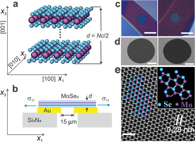
a) Scheme of MoSe2 crystal lattice, where d = Nc/2 denotes the thickness of the membrane (N stands for number of layers and c = 1.29 nm,[ 35 ] is the lattice constant along [001]). Two non‐zero in‐plane components of the stress tensor are denoted by σ11 = σ22. b) Schematic side view of the MoSe2 membrane suspended over circular (15 μm in diameter) hole in gold‐coated Si3N4 substrate. c) Optical microscopy and d) SEM images of exemplary samples. Scale bars in (c) and (d) are 20 and 5 μm, respectively. e) Atomic‐resolution TEM image of exemplary MoSe2 membrane. Scale bar in (e) is 1 nm.
To determine the elastic constants of bulk MoSe2, we performed μ‐BLS experiments in the backscattering geometry, illustrated in Figure 2a. We used p–p and s–p (p–s) polarization regarding incident‐scattered light, where p and s correspond to the polarization of the light being parallel (TM polarization) and normal (TE polarization) to the sagittal plane, respectively. As a light source, we used a single‐mode laser of wavelength λ = 523 nm, for which the real and the imaginary parts of the refractive index are n 1 = 4.7995 and n 2 = 2.0796, respectively.[ 41 ] In Figures 2a and 3a k i, and k s denote the wave vectors for the incident and scattered light, respectively, while θ is the incident angle. The surface and bulk acoustic wave vectors are represented with q and Q , respectively. A BLS experiment performed on homogeneous semiconductors allows probing Rayleigh surface waves (RSWs), pseudo‐RSWs, bulk acoustic waves (BAWs) and so‐called high‐frequency pseudo‐surface acoustic waves (HFPSAWs).[ 42 ] Figure 2a displays schematics of displacement profiles for RSWs and BAWs, that is, longitudinal (L) and transverse (T1, T2) waves, relevant for the further discussion. Figure 2b,c displays exemplary BLS spectra recorded for bulk MoSe2 at θ = 45° and light polarized in p–p and p–s configurations, respectively. As shown in Figure 2b, the BLS spectrum recorded in the p–p polarization reveals two peaks which we assigned to RSW and HFPSAW.[ 42 ] RSWs propagate in close vicinity of the free surface and contribute to BLS spectra mostly due to the surface ripple (SR) mechanism. In this case, the acoustic wave vector q lies in the free surface, and its magnitude is q = 4πsinθ/λ due to momentum conservation that holds only for the in‐plane components.[ 34 , 43 , 44 ] By changing the θ, we measured the dispersion relation of RSWs, that is, their frequency f as a function of q that is plotted in Figure 2d. Here, from the BLS data linear fit, we determined the phase velocity of RSW as v RSW = 1620 ± 13 ms−1. For the (001) plane of the hexagonal symmetry materials, v RSW can be calculated from:[ 45 ]
| (1) |
where ρ = 6900 kgm−3 denotes the mass density of MoSe2.[ 14 ] Employing this formula, we calculated v RSW using theoretically predicted elastic constants available in the literature.[ 39 , 40 ] In Figure 2d, the light blue shading stands for the range of dispersion relations that correspond to the calculated v RSW. As we can notice, the BLS results are in this range but close to its lower limit. This can be explained by an overestimation of the theoretical values discussed later in this work.
Figure 2.
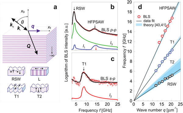
a) Schematic illustration of BLS backscattering geometry and the deformations corresponding to Rayleigh surface wave (RSW), longitudinal (L), and transverse waves (T1 and T2) bulk acoustic waves (BAWs). Symbols k i, k s, q , and Q denote incident light, scattered light, surface acoustic, and bulk acoustic wave vectors, respectively, while θ is the incident angle. b,c) Experimental and calculated BLS spectra for bulk MoSe2 obtained at θ = 45° for p–p polarization (b) and s–p polarization (c). Symbols I 1, I 2, and I 3 stand for the calculated BLS intensity corresponding to acoustic waves of polarization in x 1, x 2, and x 3 axes, respectively (Section S4.2, Supporting Information for details). HFPSAW denotes high‐frequency pseudo‐surface acoustic wave while the red arrow stands for the L BAW threshold. d) The measured dispersion relation for observed modes (circles) and their fitting (solid lines) for the bulk MoSe2. The shaded regions indicate dispersions calculated according to theoretical data available in the literature.[ 39 , 40 ]
Figure 3.
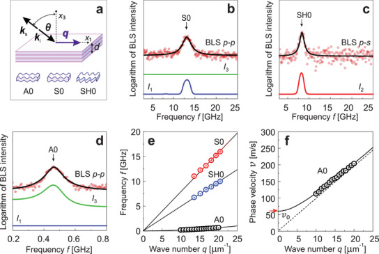
a) Schematics of the backscattering BLS geometry and displacements of the fundamental antisymmetric (A0), symmetric (S0 Lamb), and shear horizontal (SH0) waves. b–d) Normalized experimental and calculated BLS spectra of 6.9 nm‐thick MoSe2 membrane obtained at θ = 45°. e) Experimental (circles) and theoretical (solid lines) dispersion relation obtained for 6.9 nm‐thick MoSe2 membrane. f) Experimental (circles) and calculated (solid line) v(q) dispersion relation of the A0 mode. The red arrow indicates the cut‐off phase velocity v 0. The dashed line denotes the calculated v(q) dispersion relation of A0 mode for σ0 = 0.
The HFPSAW is a leaky surface wave of pronounced longitudinal polarization and displacement field localized close to the free surface. HFPSAWs, also known as longitudinal resonances[ 42 ] or skimming longitudinal waves,[ 46 ] can propagate with velocities almost identical to that of L BAWs. Their detection by BLS is possible only for highly opaque materials due to sub‐surface photo‐elastic (PE) coupling.[ 42 ] However, this requires strong suppression of usual bulk BLS backscattering (Figure 2a) from bulk acoustic waves with the wave number Q = 4πn 1/λ. This condition is met for MoSe2 as the penetration depth of light (532 nm) is δ p = λ/4πn 2 = 20 nm and hence the relevant peak is not detected by BLS (Figure S6, Supporting Information). The sub‐surface PE coupling also enables detection of the fast transverse wave (T1) wave in the s–p BLS configuration as evident in Figure 2c. Both HFPSAW and T1 waves have been previously detected using BLS in GaAs [ 42 ] and other vdW materials.[ 29 ] Notably, their acoustic wave vectors are identical to that of RSW, and thereby, their phase velocities can be directly determined from the dispersion relations f(q) plotted in Figure 2d. In this way, we calculated the velocities of HFPSAW and T1 modes as v HFPSAW = 5256 ± 38 ms−1 and v T1 = 3209 ± 19 ms−1, respectively. These values are reasonable with respect to v RSW and in good agreement with the theoretical literature data (shaded areas in Figure 2d).[ 39 , 40 ]
For a hexagonal crystal belonging to the space group, the phase velocities of L, T1, and T2 waves propagating in (001) are given as v L = (C 11/ρ)1/2, v T1 = (C 66/ρ)1/2, and v T2 = (C 44/ρ)1/2,[ 47 ] respectively. Here, we assume that the velocity of HFPSAW coincidences with the longitudinal velocity (v HFPSAW = v L).[ 29 , 42 ] Hence, from the measured velocities, we obtained the elastic constants GPa and GPa. Further, from C 11 and C 66, we determined C 12 = C 11 − 2C 66 = 49 ± 4 GPa. Although T2 cannot be resolved in our experiment due to selection rules[ 42 , 47 ] (Section S4.2, Supporting Information), we deduced C 44 from the measured phase velocity of RSW. Since the v RSW is mostly sensitive to C 44 and only weakly dependent on C 13 and C 33,[ 48 ] (Figure S7, Supporting Information), we calculate the elastic constant from Equation (1). Thus, using C 11 determined from BLS and taking for consistency C 13 = 9.8 GPa and C 33 = 54.9 GPa from the literature,[ 30 , 39 ] we obtained C 44 = 18.8 ± 0.7 GPa. The latter deviates from predictions of DFT theory in the literature, namely C 44 = 32.9 GPa[ 39 ] and C 44 = 15.9 GPa.[ 40 ] This difference explains the discrepancy between measured and predicted dispersions of RSW evident in Figure 2d. However, C 44 obtained in this work agrees well with previous Raman studies finding C 44 = 17.75 ± 1.9 GPa.[ 24 , 32 ] Previously reported theoretical and experimental elastic constants of bulk MoSe2 are listed in Table S5, Supporting Information. The elastic constants determined from BLS are positive and satisfy the thermodynamic stability criteria.[ 49 ] From the perspective of other vdW materials (Table S6, Supporting Information), the elasticity of bulk MoSe2 is typical for the TMDCs family. In principle, C 11 that corresponds to the in‐plane elasticity is significantly larger than the out‐of‐plane component given by C 33 due to the weak interactions between the layers. In Figure 2b,c we compared experimental data with the BLS spectra calculated employing the elastodynamic Green's functions at the free surface (x 3 = 0) and using the measured C ij .[ 42 , 43 , 44 ] The calculated and experimental spectra consistent in terms of the peak positions and spectral lineshapes. In particular, the peak associated with HFPSAW is centered at the frequency that coincides with L BAW threshold (red arrow in Figure 2b), which justifies the assumption regarding the equality of velocities for these waves. The details of the calculations and further discussion of the spectral lineshapes are provided in Section S4.2, Supporting Information.
To evaluate the elastic properties of a few‐layer MoSe2 membranes with varying thicknesses, we applied the backscattering BLS geometry as shown in Figure 3a. In this case, the magnitude of the acoustic wave vector is defined again as q = 4πsinθ/λ.[ 50 , 51 , 52 ] Under spatial confinement of the medium in one direction, the BAWs turn into families of symmetric (S), antisymmetric (A) Lamb, and shear‐horizontal (SH) waves. The zero‐order (fundamental) modes relevant for this work are illustrated in Figure 3a.[ 53 , 54 ]
Figure 3b,c displays measured and calculated BLS spectra of A0 and S0 waves (p–p polarization) for 6.9 nm‐thick MoSe2 membrane. Changing polarization to p–s or s–p allows us to resolve SH0, as illustrated in Figure 3d. The peaks are fitted with Lorentzian functions to determine their spectral positions. As for the bulk, we performed angle‐resolved BLS experiments to evaluate the elastic properties of the membranes. Figure 3e displays the dispersion relations f(q) of A0, SH0, and S0 modes propagating in the MoSe2 membrane. For the measured range of wave numbers, the dispersion relations of S0 and SH0 modes are linear and do not depend directly on the membrane thickness (Figure S11, Supporting Information). Therefore, S0 and SH0 waves are identical to L and T1 waves of bulk MoSe2, and their phase velocities are given by v S0 = (C 11/ρ)1/2 and v SH0 = (C 66/ρ)1/2, respectively. In practice, this allows for the straightforward evaluation of C 11 and C 66 of the membranes.
In general, for small, reduced wavenumbers (qd → 0), the dispersion relation f(q) of the A0 mode is parabolic (f ∝ q 2). This implies a linear dependence (v ∝ q) of the phase velocity v = 2πf/q on the wave number q.[ 50 , 51 , 54 ] However, the experimental v(q) of the A0 mode plotted in Figure 3f deviates from the expected linear trend (dashed line) what can be explained by the residual stress in the membrane. The latter can be well‐estimated from the cut‐off phase velocity v 0(qd → 0) = (σ 0/ρ)1/2 fitted from the dispersion v(q) plotted in Figure 3f.[ 51 ] For the considered acoustic wavelengths, being much larger than the membrane thickness, the dispersion relation of A0 mode mostly depends on three parameters: C 11, σ 0 and d, while the effect of the remaining constants is negligible (Figure S12, Supporting Information). Thus, the dispersion of the A0 mode can be used to determine the membrane thickness. In principle, for anisotropic materials, this requires a numerical approach described in Section S4.3, Supporting Information, with thickness and residual stress as the fitting parameters. The d and σ 0 obtained in this way are listed in Table S4, Supporting Information, and compared with the results of Raman spectroscopy, AFM, and optical contrast method. In particular, the thickness‐dependent frequency of the A1g Raman mode is consistent with the thickness measured using BLS (Section S5 and Figure S10, Supporting Information). In terms of the absolute values, we found good agreement between the results from AFM and optical contrast measurements and the values extracted from BLS data. Therefore, μ‐BLS provides a new contactless means for evaluating the thickness and residual stress of ultrathin membranes and can be an alternative or a supporting method for more established techniques. Further details and discussion can be found in Sections S1, S4.3, and S5, Supporting Information.
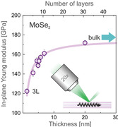
Figure 4 displays measured C 11, C 66, and E 11 (in‐plane component, details in Section S8, Supporting Information) as a function of the membrane thickness (number of layers) and compared with the literature values.[ 33 , 39 , 40 , 55 , 56 ] To the best of our knowledge, elastic constants of a few‐layer and bulk MoSe2 presented in this work are the first obtained from a direct experiment. As we can notice from Figure 4, all three elastic parameters monotonically decrease with reducing the membrane thickness. This apparent softening of the material is indicative of the so‐called elastic size effect in vdW materials.[ 15 , 16 , 17 , 18 , 57 , 58 , 59 ] To date, this phenomenon remains controversial as the experimental studies have not concluded whether the nanoconfinement results in softening or stiffening. The prior works employing diverse techniques have reported somewhat scattered values of averaged Young modulus (see Table S8, Supporting Information).[ 15 , 18 , 23 , 25 , 27 , 28 , 58 , 60 , 61 , 62 , 63 , 64 , 65 , 66 ] The anisotropic elasticity probed by Raman spectroscopy has revealed that C 44 and C 33 constants remain the same for 2D MoS2 with respect to the bulk.[ 67 ] This approach is, however, indirect and simplifies interlayer interactions to a linear chain model. On the other hand, our finding goes hand in hand with the recent femtosecond pump–probe measurements of MoSe2 revealing the softening of C 33 with a reducing number of layers.[ 30 ]
Figure 4.
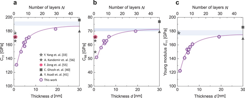
a,b) Elastic constants C 11 (a), andC 66 (b), and c) in‐plane Young modulus E 11 as a function of the membrane thickness (number of layers). The open circles in (a–c) are from the experimental data in this work, while the other symbols (stars) stand for the single‐layer theoretical data found in the literature.[ 33 , 55 , 56 ] Bulk elastic properties obtained in this work and from the theoretical data found in the literature[ 39 , 40 ] are denoted in (a–c) by shaded areas and symbols (triangles, squares), respectively. The solid lines are guides to the eye.
For specific techniques and engineering problems, the Young modulus and Poisson ratio are much more common than the elastic tensor. We used the experimental results to calculate the in‐plane component E 11 of the Young modulus (Section S8, Supporting Information). This parameter is more convenient for comparison with the values obtained by other techniques. According to BLS data plotted in Figure 4c, E 11 systematically decreases with a reducing number of layers from 177 ± 4 GPa for bulk to 122 ± 3 GPa for 2L MoSe2. Our results significantly differ from the size‐independent Young modulus E = 224 ± 41 GPa obtained by the buckling metrology for 5–10L MoSe2.[ 26 ] Also, a very recent, in situ tensile testing has evaluated the in‐plane Young modulus of one‐ and two‐layer free‐standing MoSe2 as E = 177.2 ± 9.3 GPa.[ 33 ] Notably, the latter value is consistent with E 11 of bulk MoSe2 obtained in our study, albeit the limited number of samples does not allow for any statement regarding the elastic size effect.[ 33 ] We note that the residual stress cannot explain the behavior observed in Figure 4 as it does not correlate with the membrane thickness, and in principle, it is too low (from 0 to 188 MPa) to affect the elastic constants due to the elastic nonlinearity.[ 54 , 68 ]
Overall, BLS of acoustic phonons in MoSe2 shows a considerable reduction of elastic constants with decreasing the number of layers (Figure 4). Notably, this behavior goes hand in hand with the red‐shift of the A1g Raman mode in ultrathin TMDCs (Section S5, Supporting Information). The latter was explained in prior works as resulting from softening of the effective restring forces acting on the atoms due to decreased vdW interlayer interactions with reducing the number of layers.[ 69 , 70 ] Nevertheless, a comprehensive understanding of the size‐effect reported in this work requires further experiments and theoretical modeling.
3. Conclusions
We applied micro‐Brillouin light scattering to investigate dispersion relations of GHz acoustic waves in single‐crystal bulk and few‐layer thick MoSe2 down to three molecular layers. In this way, we determined the elastic constants C 11, C 66 being consistent with prior theoretical predictions, and C 44 in good agreement with the values obtained from Raman spectroscopy. To the best of our knowledge, these elastic constants have been directly measured for the first time, even though MoSe2 is a prototypical and heavily studied member of the TMDCs family. Next, we employed μ‐BLS to study the dispersion of acoustic Lamb waves propagating in MoSe2 membranes and determined C 11, C 66, E 11, and membrane thickness. We observed a significant elastic softening of MoSe2 with decreasing the numbers of layers, which is already clearly discernible for 10L. This elastic size effect can have profound implications for the accurate design, construction, and control of nanodevices, for example, nanomechanical resonators for sensors. Also, modified elasticity at the nanoscale should affect phononic thermal transport, and hence it has significant consequences for the thermal conductivity of TMDCs. Finally, by all the above and thorough comparison of the existing experimental studies, we note that elastic size effects might be present in other TMDCs but remain unnoticed due to inconsistent results from the various experimental approaches.
4. Experimental Section
Materials
Bulk 2H‐MoSe2 was purchased from HQ Graphene. A custom‐built dry‐transfer stage, inspired by the design of Castellanos‐Gomez et al.,[ 71 ] was used to transfer MoSe2 flakes of different thicknesses (in the range from 1 to 20 nm) over large‐area (175 μm2) holes. First, bulk flakes of MoSe2 were mechanically exfoliated by Scotch tape onto an about 1 mm‐thick PDMS stamp, made by mixing silicone curing agent and elastomer (SYLGARD, in 1:10 proportions). The clean, transparent PDMS allowed optical thickness identification, alignment, and transfer of suitable flakes over single‐hole (15 μm), silicon nitride windows (Norcada, NTPR005D‐C15). The transfer yield was increased by gold‐coating the target substrates with 5/50 nm of Ti/Au in an E‐beam evaporator (AJA Orion), thanks to the enhanced adhesion of TMDCs on gold surfaces.[ 72 ] It was crucial to use high‐quality, crystalline flakes (with sharp edges, no cracks or wrinkles) and to release them very gently through the suspended region to avoid their collapse at the point of transfer. Scanning electron Micrographs (SEM) were obtained under low current conditions (1 kV) in a 7001TTLS (JEOL) instrument. Finally, high‐resolution transmission electron microscopy (HR‐TEM) images were collected at 80 kV in an ARM‐200f (JEOL) equipment. The thicknesses were determined by the optical contrast method and AFM (Section S1, Supporting Information). AFM measurements (Figure S5, Supporting Information) on the suspended regions of the MoSe2 flake showed sub‐nanometer flatness over several microns, confirming the absence of small (sub‐micrometer) wrinkles.
Brillouin Light Scattering
For the backscattering experiment, CW laser (Spectra‐Physics, Excelsior 300) of wavelength λ = 532 nm and low power (about 100 μW for thin up to 750 μW for the thickest free‐standing sample) was used as the light source. Laser light was partially reflected from the pellicle beamsplitter (R:T,8:92) and then focused on the sample, with the incident angle θ, by 20× long WD microscope objective. In the used geometry, the same objective collected the scattered light, which was focused on the pinhole (aperture was set to be 3 mm, depending on the particular sample) of a Fabry–Perot interferometer (JRS Scientific Instruments). The beam spot size on the samples was less than 1 μm, which was much less than the diameter of the membrane. Thus, it allowed the evaluation of mechanical properties from flat parts of the membranes. (Figure S1, Supporting Information).
Conflict of Interest
The authors declare no conflict of interest.
Supporting information
Supporting Information
Acknowledgements
The work was supported by the Foundation for Polish Science (POIR.04.04.00‐00‐5D1B/18). ICN2 was supported by the Severo Ochoa program from Spanish MINECO (Grant No. SEV‐2017‐0706). K.J.T. acknowledges funding from the European Union's Horizon 2020 research and innovation program under Grant Agreement No. 804349 (ERC StG CUHL), RyC fellowship No. RYC‐2017‐22330 and IAE project PID2019‐111673GB‐I00. E.C. acknowledges the partial financial support from the National Science Centre (NCN) of Poland by the OPUS grant 2019/35/B/ST5/00248.
Open access funding enabled and organized by Projekt DEAL.
Babacic V., Saleta D. Reig, Varghese S., Vasileiadis T., Coy E., Tielrooij K. J., Graczykowski B., Thickness‐Dependent Elastic Softening of Few‐Layer Free‐Standing MoSe2 . Adv. Mater. 2021, 33, 2008614. 10.1002/adma.202008614
The copyright line for this article was changed on 15 June 2021 after original online publication.
Data Availability Statement
The data that support the findings of this study are available from the corresponding author upon reasonable request.
References
- 1. Wang Q. H., Kalantar‐Zadeh K., Kis A., Coleman J. N., Strano M. S., Nat. Nanotechnol. 2012, 7, 699. [DOI] [PubMed] [Google Scholar]
- 2. Zhang Y., Chang T.‐R., Zhou B., Cui Y.‐T., Yan H., Liu Z., Schmitt F., Lee J., Moore R., Chen Y., Lin H., Jeng H.‐T., Mo S.‐K., Hussain Z., Bansil A., Shen Z.‐X., Nat. Nanotechnol. 2014, 9, 111. [DOI] [PubMed] [Google Scholar]
- 3. Morell N., Reserbat‐Plantey A., Tsioutsios I., Schädler K. G., Dubin F., Koppens F. H. L., Bachtold A., Nano Lett. 2016, 16, 5102. [DOI] [PMC free article] [PubMed] [Google Scholar]
- 4. Rhyee J.‐S., Kwon J., Dak P., Kim J. H., Kim S. M., Park J., Hong Y. K., Song W. G., Omkaram I., Alam M. A., Kim S., Adv. Mater. 2016, 28, 2316. [DOI] [PubMed] [Google Scholar]
- 5. Roy A., Movva H. C. P., Satpati B., Kim K., Dey R., Rai A., Pramanik T., Guchhait S., Tutuc E., Banerjee S. K., ACS Appl. Mater. Interfaces 2016, 8, 7396. [DOI] [PubMed] [Google Scholar]
- 6. Eftekhari A., Appl. Mater. Today 2017, 8, 1. [Google Scholar]
- 7. Yang J., Wang Z., Wang F., Xu R., Tao J., Zhang S., Qin Q., Luther‐Davies B., Jagadish C., Yu Z., Lu Y., Light Sci. Appl. 2016, 5, e16046. [DOI] [PMC free article] [PubMed] [Google Scholar]
- 8. Hu F., Luan Y., Scott M. E., Yan J., Mandrus D. G., Xu X., Fei Z., Nat. Photon. 2017, 11, 356. [Google Scholar]
- 9. Zhang H., Abhiraman B., Zhang Q., Miao J., Jo K., Roccasecca S., Knight M. W., Davoyan A. R., Jariwala D., Nat. Commun. 2020, 11, 3552. [DOI] [PMC free article] [PubMed] [Google Scholar]
- 10. Munkhbat B., Baranov D. G., Stührenberg M., Wersäll M., Bisht A., Shegai T., ACS Photonics 2019, 6, 139. [Google Scholar]
- 11. Lin H., Xu Z.‐Q., Cao G., Zhang Y., Zhou J., Wang Z., Wan Z., Liu Z., Loh K. P., Qiu C.‐W., Bao Q., Jia B., Light Sci. Appl. 2020, 9, 137. [DOI] [PMC free article] [PubMed] [Google Scholar]
- 12. Nicolosi V., Chhowalla M., Kanatzidis M. G., Strano M. S., Coleman J. N., Science 2013, 340, 1226419. [Google Scholar]
- 13. Li H., Wu J., Yin Z., Zhang H., Acc. Chem. Res. 2014, 47, 1067. [DOI] [PubMed] [Google Scholar]
- 14. Morell N., Tepsic S., Reserbat‐Plantey A., Cepellotti A., Manca M., Epstein I., Isacsson A., Marie X., Mauri F., Bachtold A., Nano Lett. 2019, 19, 3143. [DOI] [PubMed] [Google Scholar]
- 15. Bertolazzi S., Brivio J., Kis A., ACS Nano 2011, 5, 9703. [DOI] [PubMed] [Google Scholar]
- 16. Choudhary K., Cheon G., Reed E., Tavazza F., Phys. Rev. B 2018, 98, 014107. [DOI] [PMC free article] [PubMed] [Google Scholar]
- 17. Liu K., Wu J., J. Mater. Res. 2016, 31, 832. [Google Scholar]
- 18. Falin A., Cai Q., Santos E. J., Scullion D., Qian D., Zhang R., Yang Z., Huang S., Watanabe K., Taniguchi T., Barnett M. R., Chen Y., Ruoff R. S., Li L. H., Nat. Commun. 2017, 8, 15815. [DOI] [PMC free article] [PubMed] [Google Scholar]
- 19. Cai Y., Ke Q., Zhang G., Feng Y. P., Shenoy V. B., Zhang Y.‐W., Adv. Funct. Mater. 2015, 25, 2230. [Google Scholar]
- 20. Skolnick M. S., Roth S., Alms H., J. Phys. C: Solid State Phys. 1977, 10, 2523. [Google Scholar]
- 21. Gatulle M., Fischer M., Chevy A., Phys. Status Solidi B 1983, 119, 327. [Google Scholar]
- 22. Kim T., Ding D., Yim J.‐H., Jho Y.‐D., Minnich A. J., APL Mater. 2017, 5, 086105. [Google Scholar]
- 23. Bosak A., Krisch M., Mohr M., Maultzsch J., Thomsen C., Phys. Rev. B 2007, 75, 153408. [Google Scholar]
- 24. Zhang X., Tan Q.‐H., Wu J.‐B., Shi W., Tan P.‐H., Nanoscale 2016, 8, 6435. [DOI] [PubMed] [Google Scholar]
- 25. Feldman J., J. Phys. Chem. Solids 1976, 37, 1141. [Google Scholar]
- 26. Iguiñiz N., Frisenda R., Bratschitsch R., Castellanos‐Gomez A., Adv. Mater. 2019, 31, 1807150. [DOI] [PubMed] [Google Scholar]
- 27. Suk J. W., Hao Y., Liechti K. M., Ruoff R. S., Chem. Mater. 2020, 32, 6078. [Google Scholar]
- 28. Davidovikj D., Alijani F., Cartamil‐Bueno S. J., van der Zant H. S. J., Amabili M., Steeneken P. G., Nat. Commun. 2017, 8, 1253. [DOI] [PMC free article] [PubMed] [Google Scholar]
- 29. Harley R. T., Fleury P. A., J. Phys. C: Solid State Phys. 1979, 12, L863. [Google Scholar]
- 30. Soubelet P., Reynoso A. A., Fainstein A., Nogajewski K., Potemski M., Faugeras C., Bruchhausen A. E., Nanoscale 2019, 11, 10446. [DOI] [PubMed] [Google Scholar]
- 31. Hadland E. C., Jang H., Wolff N., Fischer R., Lygo A. C., Mitchson G., Li D., Kienle L., Cahill D. G., Johnson D. C., Nanotechnology 2019, 30, 285401. [DOI] [PubMed] [Google Scholar]
- 32. Kuzuba T., Ishii M., Phys. Status Solidi B 1989, 155, K13. [Google Scholar]
- 33. Yang Y., Li X., Wen M., Hacopian E., Chen W., Gong Y., Zhang J., Li B., Zhou W., Ajayan P. M., Chen Q., Zhu T., Lou J., Adv. Mater. 2017, 29, 1604201. [DOI] [PubMed] [Google Scholar]
- 34. Carlotti G., Appl. Sci. 2018, 8, 124. [Google Scholar]
- 35. James P. B., Lavik M. T., Acta. Cryst. 1963, 16, 1183. [Google Scholar]
- 36. Auld B. A., Acoustic Fields and Waves in Solids, vol. 1, Wiley, New York, 1973. [Google Scholar]
- 37. Frisenda R., Navarro‐Moratalla E., Gant P., Pérez De Lara D., Jarillo‐Herrero P., Gorbachev R. V., Castellanos‐Gomez A., Chem. Soc. Rev. 2018, 47, 53. [DOI] [PubMed] [Google Scholar]
- 38. Chen Z., Liu H., Chen X., Chu G., Chu S., Zhang H., ACS Appl. Mater. Interfaces 2016, 8, 20267. [DOI] [PubMed] [Google Scholar]
- 39. Ghosh C. K., Sarkar D., Mitra M. K., Chattopadhyay K. K., J. Phys. D: Appl. Phys. 2013, 46, 395304. [Google Scholar]
- 40. Asadi Y., Nourbakhsh Z., J. Elec. Materi. 2019, 48, 7977. [Google Scholar]
- 41. Beal A. R., Hughes H. P., J. Phys. C: Solid State Phys. 1979, 12, 881. [Google Scholar]
- 42. Mutti P., Bottani C. E., Ghislotti G., Beghi M., Briggs G. A. D., Sandercock J. R., Surface Brillouin Scattering—Extending Surface Wave Measurements to 20 GHz, Springer US, Boston, MA, USA: 1995, pp. 249–300. [Google Scholar]
- 43. Every A. G., Comins J. D., In Handbook of Advanced Nondestructive Evaluation (Eds: Ida N., Meyendorf N.), Springer International Publishing, Cham, Switzerland: 2019, pp. 327–359. [Google Scholar]
- 44. Every A., Mathe B., Comins J., Ultrasonics 2006, 44, e929. [DOI] [PubMed] [Google Scholar]
- 45. Lee S. A., Lindsay S. M., Phys. Status Solidi B 1990, 157, K83. [Google Scholar]
- 46. Lomonosov A. M., Yan X., Sheng C., Gusev V. E., Ni C., Shen Z., Phys. Status Solidi RRL 2016, 10, 606. [Google Scholar]
- 47. Laser Handbook (Eds: Arecchi F. T., Schulz‐Dubois E. O.) Vol. 1, North‐Holland Publ. Co, Amsterdam, The Netherlands, reprinted edition 1988. [Google Scholar]
- 48. Carlotti G., Fioretto D., Socino G., Verona E., J. Phys.: Condens. Matter. 1995, 7, 9147. [Google Scholar]
- 49. Mouhat F., Coudert F.‐X., Phys. Rev. B 2014, 90, 224104. [Google Scholar]
- 50. Cuffe J., Chávez E., Shchepetov A., Chapuis P.‐O., El Boudouti E. H., Alzina F., Kehoe T., Gomis‐Bresco J., Dudek D., Pennec Y., Djafari‐Rouhani B., Prunnila M., Ahopelto J., Sotomayor Torres C. M., Nano Lett. 2012, 12, 3569. [DOI] [PubMed] [Google Scholar]
- 51. Graczykowski B., Sledzinska M., Placidi M., Saleta Reig D., Kasprzak M., Alzina F., Sotomayor Torres C. M., Nano Lett. 2017, 17, 7647. [DOI] [PubMed] [Google Scholar]
- 52. Graczykowski B., Gueddida A., Djafari‐Rouhani B., Butt H.‐J., Fytas G., Phys. Rev. B 2019, 99, 165431. [Google Scholar]
- 53. Lamb H., Proc. R. Soc. London, Ser. A 1917, 93, 114. [Google Scholar]
- 54. Graczykowski B., Gomis‐Bresco J., Alzina F., S Reparaz J., Shchepetov A., Prunnila M., Ahopelto J., M Sotomayor Torres C., New J. Phys. 2014, 16, 073024. [Google Scholar]
- 55. Zeng F., Zhang W.‐B., Tang B.‐Y., Chinese Phys. B 2015, 24, 097103. [Google Scholar]
- 56. Kandemir A., Yapicioglu H., Kinaci A., Çağin T., Sevik C., Nanotechnology 2016, 27, 055703. [DOI] [PubMed] [Google Scholar]
- 57. Chitara B., Ya'akobovitz A., Nanoscale 2018, 10, 13022. [DOI] [PubMed] [Google Scholar]
- 58. Castellanos‐Gomez A., Poot M., Steele G. A., van der Zant H. S. J., Agraït N., Rubio‐Bollinger G., Adv. Mater. 2012, 24, 772. [DOI] [PubMed] [Google Scholar]
- 59. Zhan H., Guo D., Xie G., Nanoscale 2019, 11, 13181. [DOI] [PubMed] [Google Scholar]
- 60. Blakslee O. L., Proctor D. G., Seldin E. J., Spence G. B., Weng T., J. Appl. Phys. 1970, 41, 3373. [Google Scholar]
- 61. Lee J.‐U., Yoon D., Cheong H., Nano Lett. 2012, 12, 4444. [DOI] [PubMed] [Google Scholar]
- 62. Metten D., Federspiel F., Romeo M., Berciaud S., Phys. Rev. Appl. 2014, 2, 054008. [Google Scholar]
- 63. Lee C., Wei X., Kysar J. W., Hone J., Science 2008, 321, 385. [DOI] [PubMed] [Google Scholar]
- 64. Nicholl R. J., Conley H. J., Lavrik N. V., Vlassiouk I., Puzyrev Y. S., Pantelides V. P. Sreenivas, S. T., Bolotin K. I., Nat. Commun. 2015, 6, 8789. [DOI] [PMC free article] [PubMed] [Google Scholar]
- 65. Frank I. W., Tanenbaum D. M., van der Zande A. M., McEuen P. L., J. Vac. Sci. Technol. B 2007, 25, 2558. [Google Scholar]
- 66. Cooper R. C., Lee C., Marianetti C. A., Wei X., Hone J., Kysar J. W., Phys. Rev. B 2013, 87, 035423. [Google Scholar]
- 67. Zhao Y., Luo X., Li H., Zhang J., Araujo P. T., Gan C. K., Wu J., Zhang H., Quek S. Y., Dresselhaus M. S., Xiong Q., Nano Lett. 2013, 13, 1007. [DOI] [PubMed] [Google Scholar]
- 68. Dunstan D. J., Bosher S. H. B., Downes J. R., Appl. Phys. Lett. 2002, 80, 2672. [Google Scholar]
- 69. Lee C., Yan H., Brus L. E., Heinz T. F., Hone J., Ryu S., ACS Nano 2010, 4, 2695. [DOI] [PubMed] [Google Scholar]
- 70. Liang L., Meunier V., Nanoscale 2014, 6, 5394. [DOI] [PubMed] [Google Scholar]
- 71. Castellanos‐Gomez A., Buscema M., Molenaar R., Singh V., Janssen L., van der Zant H. S. J., Steele G. A., 2D Mater. 2014, 1, 011002. [Google Scholar]
- 72. Desai S. B., Madhvapathy S. R., Amani M., Kiriya D., Hettick M., Tosun M., Zhou Y., Dubey M., Ager J. W., Chrzan D., Javey A., Adv. Mater. 2016, 28, 4053. [DOI] [PubMed] [Google Scholar]
Associated Data
This section collects any data citations, data availability statements, or supplementary materials included in this article.
Supplementary Materials
Supporting Information
Data Availability Statement
The data that support the findings of this study are available from the corresponding author upon reasonable request.