Abstract
Quantum spin Hall insulators have attracted significant attention in recent years. Understanding the optical properties and spin Hall effect in these materials is crucial for technological advancements. In this study, we present theoretical analyses to explore the optical properties, Berry curvature and spin Hall conductivity of pristine and perturbed PbBiI using the linear combination of atomic orbitals and the Kubo formula. The system is not centrosymmetric and it is hosting at the same time Rashba spin-splitting and quantized spin Hall conductivity. Our calculations reveal that the electronic structure can be modified using staggered exchange fields and electric fields, leading to changes in the optical properties. Additionally, the spin Berry curvature and spin Hall conductivity are investigated as a function of the energy and temperature. The results indicate that due to the small dynamical spin Hall conductivity, generating an ac spin current in the PbBiI requires the use of external magnetic fields or magnetic materials.
Subject terms: Nanoscience and technology, Condensed-matter physics
Introduction
In the realm of condensed matter physics, the emergence of topological materials has ushered in a new era of exploration, leading to the discovery of quantum phenomena with transformative implications. Among these materials, quantum spin Hall (QSH) insulators occupy a pivotal position, representing a paradigm shift in the understanding of topologically nontrivial electronic states1. The notion of a QSH insulator was first proposed by Bernevig 
 2, reflecting a revolutionary break from conventional electronic behavior by introducing the concept of topological protection for electronic states. These materials manifest insulating behavior in bulk but host robust conducting edge states topologically protected against back-scattering by time-reversal symmetry, ushering in the promise of dissipationless electronic transport and novel spin-based functionalities3–5.
Experimental investigations have validated the existence of QSH behavior in various material platforms, ranging from one- and two-dimensional systems to designed heterostructures, expanding the horizons of potential applications of these topological electronic states6–9. These experimental efforts have illuminated the intricate interplay between topological and electronic properties at the heart of QSH insulators. Recent advances in experimental techniques, ranging from magneto-transport measurements to angle-resolved photoemission spectroscopy, have uncovered a plethora of materials showcasing QSH behavior, expanding the horizon of potential platforms for exploiting the remarkable attributes of these topological materials10,11. Such strides in materials discovery and characterization open avenues for investigating the interplay between topological electronic states and intricate quantum phenomena.
Understanding the implications of QSH insulators extends beyond fundamental physics, venturing into the realm of practical applications in electronics and spintronics. The chiral nature of the edge states in QSH insulators offers the tantalizing prospect of dissipationless spin transport, holding promise for the development of efficient spin logic and memory devices that harness the spin degrees of freedom of electrons12–15. Moreover, the intricate interplay between the topological and electronic properties of these materials underpins their potential for realizing topologically protected quantum computation and information processing16,17. Recent theoretical advances have further underscored the potential of QSH insulators in redefining the limits of electronic and spin-based functionalities. The proposals for utilizing edge states in QSH insulators have opened up new avenues for achieving dissipationless spin transport and laying the groundwork for advancements in spin-based information processing and quantum computing18,19. The foundations set forth by the theoretical models have not only provided a roadmap for understanding the fundamental behavior of QSH insulators but also set the stage for exploring their transformative implications20,21. Amid these developments, the experimental realization of the quantum spin Hall effect and the identification of materials exhibiting topologically nontrivial electronic states have paved the way for exploring unique opportunities for harnessing their extraordinary properties22,23. The ensuing synthesis of theory and experiment has propelled the field of topological electronics into a realm of unprecedented promise and potential.
The QSH insulating phase has been investigated in both centrosymmetric24–26and noncentrosymmetric systems27,28, however, there are not so many cases where the QSH coexists with the Rashba spin splitting. In this paper, we will study a system where we have both the QSH effect and Rashba spin-splitting. Large Rashba spin-splitting is found in materials formed by heavy elements with strong intrinsic SOC such as Bi, Pb, and W, among others29–32. To date, several types of QSHIs have been reported, and recently it proposed a honeycomb noncentrosymmetric QSHIs consisting of IV, V, and VII elements and Rashba-like SOC and unconventional spin texture33. Until now, the properties of this material have been well studied in the presence of various disturbances. It has been shown that the thermodynamic properties of this material can be adjusted by a staggered exchange field34. Additionally, the effect of external fields on the electronic and optical properties of this material has also been well studied35–37.
When there is no topological insulator phase, we cannot have the QSH phase but we can still have the ordinary spin Hall effect. The spin Hall conductivity (SHC) is a fundamental property of materials that describes the ability of a material to generate a spin current in response to an applied electric field38–43. This phenomenon arises from spin-orbit coupling, where the motion of electrons interacts with their spin degrees of freedom. In the presence of an electric field, electrons experience a transverse deflection due to the spin-orbit interaction, leading to the generation of a spin current perpendicular to the charge current. The SHC tensor quantifies this effect and provides valuable information about the spin dynamics in materials. Understanding and controlling the SHC is crucial for developing spintronic devices, such as spin-based transistors and memory storage devices, which rely on the manipulation of electron spins for information processing44–46.
This paper begins by exploring the theoretical background in Theory section to gain insight into the properties of the PbBiI. Next, theoretical frameworks are applied to calculate these properties in Results and discussion section, and the results are summarized in Conclusions section.
Theory
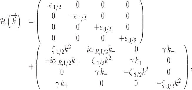
Pristine and perturbed Hamiltonian
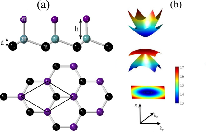
The geometric structure of the PbBiI is depicted in Fig. 1(a) with top and side views, consisting of Bi (V), Pb (IV), and I (VII) elements. The distance parameters are approximately  1.3 Å and
  = 3.04 Å. Previous analysis reveals that the highest valence comes from the
  -Bi orbitals, while the
  -Bi orbitals give the most relevant contribution to the lowest conduction band. As a result, we can ignore the Pb and I components in the electronic band structure of PbBiI. Hence, we focus on the single-particle bands with
  (p-orbitals),
  for spin angular momentum, and
  . The bands with j
 =
= 3/2 are far from the Fermi level, and we have left the bands for two spin directions with
  . Therefore, the effective Hamiltonian in the basis of
  =
= ,
, 1/2
1/2 can be expressed as:
 |
1 |
Fig. 1.
(a) Side and top view of the geometry structure of the PbBiI with Bi = V, Pb = IV, and I = VII by the buckled parameter  and Pb-I
  and Bi-Pb bond lengths 1.35 and 3.04 Å, respectively. (b) 3D band structure and contour plot of
  in the
  -
- plane.
The onsite energies are determined to be  eV and
  eV while other parameters are obtained from
 calculations33 and are
  eV/Å
eV/Å ,
,  eV/Å
eV/Å ,
,  eV/Å,
eV/Å,  eV/Å, where
  , and
, and  . The parameter
  represents the Rashba splitting in the conduction band, while
  is the spin-orbit coupling between the valence and conduction band. The PbBiI has a bulk gap of
  eV and the Rashba-like spin splitting gap
  eV in the valence bands. The spin texture around the valence bands confirms the Rashba-type spin-splitting33.
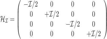
To introduce perturbations on the PbBiI system, external electric and magnetic exchange fields are applied to the Hamiltonian. The magnetic proximity effect arises from the induction of magnetic exchange fields in a material when it is in proximity to a ferromagnetic or antiferromagnetic substrate. These induced fields influence the orbital angular momentum within the basis, resulting in modifications to the Hamiltonian. Additionally, an external electric field can be applied by placing the PbBiI between two voltage gates. The modified Hamiltonian with perturbation terms  is expressed as:
 |
2 |
where  and
and  are the external staggered exchange field and electric field contributions respectively and are given by
 |
3 |
and
 |
4 |
The induced exchange field  corresponds to the total angular momentum
  (
( 47, Here,
  represents the
  -component of the 2
  2 Pauli matrix, and
  can be controlled via electric field.
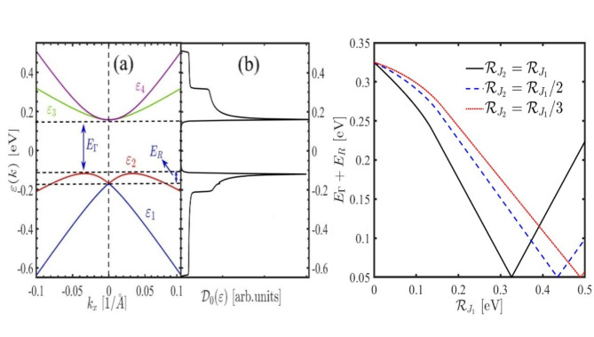
The band structure from the  effective Hamiltonian for pristine PbBiI accurately reproduces the first-principles DFT calculations33,37 reported in previous works confirming the reliability of Hamiltonian Eq. (1) and its parameters used in this paper. Figure 1 (b) and Fig. 2 (a) represent 3D and 2D band structure of the unperturbed PbBiI system, obtained from Eq. (1). This band structure comprises two valence and two conduction bands, where the valence band at the
  point is characterized by the states
  , and the effective state for the conduction band is
  . Consequently, the states include
  ,
,  ,
,  ,
,  . Total density of states of the PbBiI confirms Band structure results as depicted in Fig. 2 (b). The effect of the exchange fields on the band gap is shown if Fig. 2 (c). Applying the exchange field reduces the topological gap and finally for
  eV (which is equal to the
  ) the topological gap is completely closed and a trivial gap reopens for higher values. This is the typical signature of the band gap in QSH insulators.
Fig. 2.
(a) Band structure of the pristine PbBiI along the  direction and
  , and (b) the total density of states. (c) Band gap (
 ) as a function of different amounts of exchange fields.
Density of states
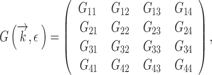
By utilizing the Green’s function approach, the density of states (DOS) for the PbBiI can be computed. The DOS can be determined by adding up over the first Brillouin zone,
 |
5 |
where  indicates the number of atoms in each unit cell. The non-interacting Green’s function matrix is acquired through
  , where
  represents the broadening factor
 |
6 |
Using Eqs. (5) and (6), the total DOS reads
 |
7 |
Optical properties
The optical conductivity tensor,  , can be determined using Ohm’s law, which states that
  , where
  is the current density,
  is the electric field, and
  is the optical conductivity tensor.
 |
8 |
To calculate  , direction-dependent velocities are required. The current operator definition along the
  direction is
 |
9 |
Also, the general form of the current operator is
 |
10 |
that  and
and  are intraband and inter-band direction-depended velocities along the
  -direction.
By using linear response theory, the optical conductivity is given as
 |
11 |
where  is the spin degeneracy,
  is photon frequency and
  is the 2D planar area.
Using Eq. (11), the interband optical conductivity is given as48–50:
 |
12 |
where  is the Fermi-Dirac distribution at a constant temperature
  and chemical potential
  ,
,  represents the eigenvalue of the energy,
  denotes the finite damping between the conduction and valence bands, and
  and
and  are velocities along the
  and
and  -directions respectively.
Another important optical property is the electron energy loss spectroscopy (EELS). The energy electron loss spectrum is a type of spectroscopy technique used to study the electronic properties of materials. It involves measuring the energy lost by electrons as they interact with a sample, which can provide information about the electronic structure and bonding of the material. The spectrum is generated by bombarding the sample with high-energy electrons and then measuring the energy distribution of the scattered electrons. The resulting spectrum can reveal details about the valence and conduction bands of the material, as well as the presence of impurities or defects. To calculate EELS, we need the dielectric function which is given by:
 |
13 |
where  is the relative permittivity and
  is the PbBiI thickness. One can calculate the EELS as
 |
14 |
We can determine the reflectivity by using the refractive index  and extinction coefficient
  and dielectric function. We have
 |
15 |
and
 |
16 |
that we have write  . Reflectivity can be calculated as
 |
17 |
Spin Hall conductivity
We calculate both static ( ) and dynamic (
 ) SHC using the Kubo formula and Berry curvatures. The component
  of the SHC tensor represents a spin current flowing along the
  -direction, polarized along the
  and an electric field applied along the
  -axis. The Kubo formula for the SHC is51,52:
 |
18 |
where dynamic spin Berry curvature, velocity, and spin-current operators are defined as
 |
19 |
and the static spin Berry curvature definition is
 |
20 |
and
 |
21 |
 |
22 |
where  while
while  and
and  are the
  Dirac matrices52.
Results and discussion
The main results of the paper are discussed in this Section. In our computational calculations we considered a 500  500 mesh points in the momentum space and
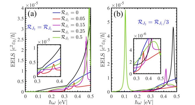
  meV. Figure 3 displays the EELS results under the influence of a staggered exchange field for varying values of
  and
and  . The range considered for
  is between 0 and 0.5 eV, while we have considered two ratios for
  =1 or 1/3. In the case where
  (as shown in Fig. 3(a)), distinct peaks are observed, and as the strength of the field increases, the peaks shift towards higher energies. Conversely, for
  (depicted in Fig. 3 (b)), an opposite shift is observed for
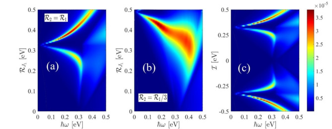
  eV. To explore the entire spectrum of staggered and electric fields, contour plots of the EELS have been calculated within a specific energy and external field range (refer to Fig. 4). Notably, the majority of EELS behavior is associated with
  and
and  eV. Comparing Fig. 4 (a) and 4 (c) reveals a similarity in the EELS response to positive values when both a staggered exchange field (
 ) and an external electric field is applied.
Fig. 3.
EELS obtained from Eq. (14) in presence of the staggered exchange field with (a)  and (b)
  .
.
Fig. 4.
Color density of the EELS in the presence of (a) the staggered exchange field with  , (b)
, (b)  and (c) external electric field.
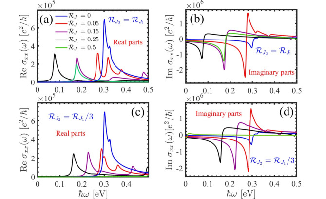
The optical conductivity of the PbBiI with external perturbations is computed using the Kubo formula. Due to the PbBiI’s isotropic nature, we focused on the optical conductivity along the  -axis and omitted the
  -axis. In the pristine case, a peak in the real part of the optical conductivity aligns with the band gap energy (see Fig. 5 (a) and 5 (c)). Adjusting the
  and
and  parameters alter the optical conductivity and shift peak energies. It is evident that regardless of the
  and
and  ratio, introducing a staggered exchange field leads to new peaks in the real parts, with only their positions changing based on different ratios. Furthermore, due to the Kramers-Kronig relation, a dip in the imaginary parts occurs at the peak’s energy in the real parts (Fig. 5 (b) and 5 (d)).
Fig. 5.
Real and imaginary parts of the optical conductivity for polarized light along the  -axis by introducing staggered exchange field (a), (b)
  and (c), (d)
  .
.
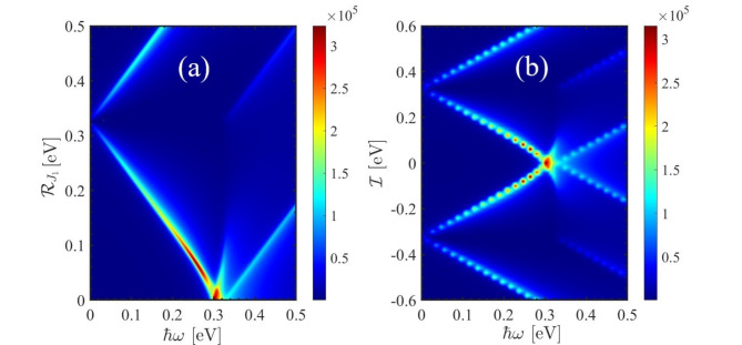
Figure 6 showcases a contour plot illustrating the optical conductivity as a function of frequency, staggered exchange field (Fig. 6 (a)), and electric field (Fig. 6 (b)). It is evident from Fig. 6 (a) that the peak of the optical conductivity appears at an energy of 0.3 eV. When  =0.3 eV, it causes a shift towards lower energies however, for
  0.3 eV this trend is reversed. The external electric field also has a similar effect except in negative magnitudes.
Fig. 6.
Color density of the real part of the optical conductivity in subject to the external perturbation (a) staggered exchange field (  ) and (b) electric field.
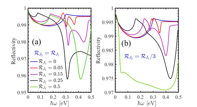
The reflectivity is defined as the ratio of the intensity of reflected light to the intensity of incident light, typically expressed as a percentage. It is a key parameter in numerous applications, including optics, coatings, architecture, and solar energy technologies, where controlling and optimizing the reflective properties of materials is essential for achieving desired performance characteristics. Figure 7 is related to the reflectivity in the presence of the staggered exchange field. As we can see by increasing the photon’s frequency, we have an increase in the reflectivity and the peaks appear. In addition, by comparing Fig. 7 (a) and 7 (b) we found that reflectivity is greater in case  .
.
Fig. 7.
Reflectivity of the perturbed PbBiI in the presence of staggered exchange field (a)  and (b)
  .
.
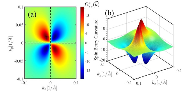
The 3D plot and color density of the spin Berry curvature of the PbBiI in the Brillouin zone are shown in Fig. 8 (a) and 8 (b) respectively. The Berry curvature is enhanced in locations where the energy difference between the bands gets reduced as in the anticrossing points. According to the figures, the Berry curvature is maximum around the  point and decreases when moving away from this point. This is due to the existence of the band crossing near the
  point.
Fig. 8.
Spin Berry curvature in the Brillouin zone around the  point in the form of (a) color density and (b) surface plot.
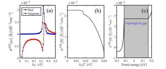
The SHC can be expressed in terms of the spin Berry curvature (see Eq. (20)). Figure 9 (a) represents the dynamical SHC of the PbBiI versus frequency. Both the real and imaginary parts of the ac SHC are small. This suggests that to generate an ac spin current, one needs to use a magnetic field or magnetic materials.
Fig. 9.
Calculated (a) real and imaginary parts of the dynamical SHC, (b) statical SHC as a function of temperature, and (c) statical SHC versus Fermi energy.
The dependence of the dc SHC on temperature is illustrated in Fig. 9 (b), however, a critical temperature of  eV is identified, beyond which the SHC decreases sharply towards room temperature, reaching a minimum for
  eV. The Spin Hall conductivity of the PbBiI as a function of Fermi energy is plotted in Fig. 9 (c). The SHC has a quantized value within the topological band gap. Our calculations reveal that the SHC is minimal at
  and extremum at
  eV. This is because there are band crossings induced by spin-orbit interactions at these specific energies.
Conclusions
In summary, we have investigated the noncentrosymmetric system PbBiI where quantized spin Hall conductivity and Rashba spin-splitting coexist. Our analysis involved the computation of the Berry curvature and spin Hall conductivity, along with investigating the electronic and optical characteristics under external influences. By introducing staggered exchange and electric fields, we were able to manipulate the optical conductivity and EELS of the PbBiI. The peak of the real part of the optical conductivity is observed at 0.3 eV, with perturbations causing a shift towards lower energies. The Berry curvature reaches its maximum near the  point where band crossing occurs, diminishing significantly further away from this region. Given the low dynamical spin Hall conductivity, a magnetic field is necessary to induce an a.c. spin current. Furthermore, the dc spin Hall conductivity exhibits critical behavior around
  eV. Also the spin-resolved optical conductivity could be one of the future research directions.
Acknowledgements
C. A. was supported by the Foundation for Polish Science project “MagTop” no. FENG.02.01-IP.05-0028/23 co-financed by the European Union from the funds of Priority 2 of theEuropean Funds for a Smart Economy Program 2021–2027 (FENG).
Author contributions
M. M. N proposed the subject and performed programming and writing and C. A contributed to formal analysis, writing - review & editing.
Data availability
The data that support the findings of this study areavailable from the corresponding author upon reasonablerequest.
Declarations
Competing interests
The authors declare no competing interests.
Footnotes
Publisher’s note
Springer Nature remains neutral with regard to jurisdictional claims in published maps and institutional affiliations.
References
- 1.Driggers, R. G., Friedman, M. H. & Nichols, J. Introduction to Infrared and electro-optical Systems (Artech House, 2012).
- 2.Bernevig, B. A. & Zhang, S. C. Quantum spin Hall effect. Phys. Rev. Lett. 96 (10), 106802 (2006). [DOI] [PubMed] [Google Scholar]
- 3.Qi, X. L. & Zhang, S. C. Topological insulators and superconductors. Rev. Mod. Phys. 83 (4), 1057–1110 (2011). [Google Scholar]
- 4.Hsieh, D. et al. A tunable topological insulator in the spin helical Dirac transport regime. Nature. 460 (7259), 1101–1105 (2009). [DOI] [PubMed] [Google Scholar]
- 5.Bercioux, D. & Lucignano, P. Quantum transport in Rashba spin–orbit materials: a review. Rep. Prog. Phys. 78 (10), 106001 (2015). [DOI] [PubMed] [Google Scholar]
- 6.Konig, M. et al. Quantum spin Hall insulator state in HgTe quantum wells. Science. 318 (5851), 766–770 (2007). [DOI] [PubMed] [Google Scholar]
- 7.Yan, B. & Zhang, S. C. Topological materials. Rep. Prog. Phys. 75 (9), 096501 (2012). [DOI] [PubMed] [Google Scholar]
- 8.Brüne, C. et al. Spin polarization of the quantum spin hall edge states. Nat. Phys. 8 (6), 485–490 (2012). [Google Scholar]
- 9.Olshanetsky, E. et al. Persistence of a two-dimensional topological insulator state in wide HgTe quantum wells. Phys. Rev. Lett. 114 (12), 126802 (2015). [DOI] [PubMed] [Google Scholar]
- 10.HaldaneF.D.M. Model for a quantum Hall effect without Landau levels: condensed-matter realization of the parity anomaly. Phys. Rev. Lett. 61 (18), 2015 (1988). [DOI] [PubMed] [Google Scholar]
- 11.Chang, C. Z. et al. Experimental observation of the quantum anomalous hall effect in a magnetic topological insulator. Science. 340 (6129), 167–170 (2013). [DOI] [PubMed] [Google Scholar]
- 12.Pesin, D. & MacDonald, A. H. Spintronics and pseudospintronics in graphene and topological insulators. Nat. Mater. 11 (5), 409–416 (2012). [DOI] [PubMed] [Google Scholar]
- 13.Liu, C. X. et al. Model Hamiltonian for topological insulators. Phys. Rev. B—Condensed Matter Mater. Phys. 82 (4), 045122 (2010). [Google Scholar]
- 14.Jansen, R. Silicon spintronics. Nat. Mater. 11 (5), 400–408 (2012). [DOI] [PubMed] [Google Scholar]
- 15.Manchon, A. et al. New perspectives for Rashba spin–orbit coupling. Nat. Mater. 14 (9), 871–882 (2015). [DOI] [PubMed] [Google Scholar]
- 16.Kitaev, A. Y. Fault-tolerant quantum computation by anyons. Ann. Phys. 303 (1), 2–30 (2003). [Google Scholar]
- 17.Nayak, C. et al. Non-abelian anyons and topological quantum computation. Rev. Mod. Phys. 80 (3), 1083–1159 (2008). [Google Scholar]
- 18.Young, S. M. & Kane, C. L. Dirac semimetals in two dimensions. Phys. Rev. Lett. 115 (12), 126803 (2015). [DOI] [PubMed] [Google Scholar]
- 19.Maciejko, J. et al. Kondo effect in the helical edge liquid of the quantum spin Hall state. Phys. Rev. Lett. 102 (25), 256803 (2009). [DOI] [PubMed] [Google Scholar]
- 20.Fu, L. Topological crystalline insulators. Phys. Rev. Lett. 106 (10), 106802 (2011). [DOI] [PubMed] [Google Scholar]
- 21.Zhang, H. et al. Topological insulators in Bi2Se3, Bi2Te3 and Sb2Te3 with a single Dirac cone on the surface. Nat. Phys. 5 (6), 438–442 (2009). [Google Scholar]
- 22.Xu, S. Y. et al. Observation of a topological crystalline insulator phase and topological phase transition in Pb1 – x Sn x Te. Nat. Commun. 3 (1), 1192 (2012). [DOI] [PubMed] [Google Scholar]
- 23.Kou, X. et al. Scale-invariant quantum anomalous hall effect in magnetic topological insulators beyond the two-dimensional limit. Phys. Rev. Lett. 113 (13), 137201 (2014). [DOI] [PubMed] [Google Scholar]
- 24.Fu, L. & Kane, C. L. Topological insulators with inversion symmetry. Phys. Rev. B—Condensed Matter Mater. Phys. 76 (4), 045302 (2007). [Google Scholar]
- 25.Islam, R. et al. Switchable large-gap quantum spin Hall state in the two-dimensional M Si 2 Z 4 class of materials. Phys. Rev. B. 106 (24), 245149 (2022). [Google Scholar]
- 26.Islam, R. et al. Fast electrically switchable large gap quantum spin Hall states in MGe2Z4. Adv. Electron. Mater. 9 (8), 2300156 (2023). [Google Scholar]
- 27.Dietl, T. Effects of charge dopants in quantum spin hall materials. Phys. Rev. Lett. 130 (8), 086202 (2023). [DOI] [PubMed] [Google Scholar]
- 28.Nguyen, N. M. et al. Unprotected edge modes in quantum spin Hall insulator candidate materials. Phys. Rev. B. 107 (4), 045138 (2023). [Google Scholar]
- 29.Hirahara, T. et al. Role of spin-orbit coupling and hybridization effects in the electronic structure format? Of Ultrathin Bi Films. Phys. Rev. Lett. 97 (14), 146803 (2006). [DOI] [PubMed] [Google Scholar]
- 30.Mathias, S. et al. Quantum-well-induced giant spin-orbit splitting. Phys. Rev. Lett. 104 (6), 066802 (2010). [DOI] [PubMed] [Google Scholar]
- 31.Yuan, H. et al. Zeeman-type spin splitting controlled by an electric field. Nat. Phys. 9 (9), 563–569 (2013). [Google Scholar]
- 32.Dil, J. H. et al. Rashba-type spin-orbit splitting of quantum well states in ultrathin pb films. Phys. Rev. Lett. 101 (26), 266802 (2008). [DOI] [PubMed] [Google Scholar]
- 33.Mera Acosta, C. et al. Unconventional spin texture in a noncentrosymmetric quantum spin Hall insulator. Phys. Rev. B. 94 (4), 041302 (2016). [Google Scholar]
- 34.Phuong, L. T. et al. Enhancement of the thermoelectric power factor in monolayer PbBiI: staggered exchange field effect. J. Mater. Chem. A. 10 (31), 16620–16626 (2022). [Google Scholar]
- 35.Phong, T. C. & Phuong, L. T. Optical refraction and absorption spectra in perturbed monolayer PbBiI. J. Appl. Phys., 132(1). (2022).
- 36.Hoi, B. D. Effect of C 3 v symmetry breaking on the noncentrosymmetric quantum spin Hall insulating phase and optical characteristics of monolayer PbBiI. Phys. Rev. B. 106 (16), 165424 (2022). [Google Scholar]
- 37.Phong, T. C., Lam, V. T. & Hoi, B. D. Tuning electronic phase in noncentrosymmetric quantum spin Hall insulators through physical stimuli. J. Phys.: Condens. Matter. 33 (32), 325502 (2021). [DOI] [PubMed] [Google Scholar]
- 38.Kato, Y. K. et al. Observation of the spin Hall effect in semiconductors. Science. 306 (5703), 1910–1913 (2004). [DOI] [PubMed] [Google Scholar]
- 39.Wunderlich, J. et al. Experimental Observation of the spin-hall effect in a two-dimensional format? Spin-Orbit coupled Semiconductor System. Phys. Rev. Lett. 94 (4), 047204 (2005). [DOI] [PubMed] [Google Scholar]
- 40.Murakami, S., Nagaosa, N. & Zhang, S. C. Dissipationless quantum spin current at room temperature. Science. 301 (5638), 1348–1351 (2003). [DOI] [PubMed] [Google Scholar]
- 41.Sinova, J. et al. Universal intrinsic spin Hall effect. Phys. Rev. Lett. 92 (12), 126603 (2004). [DOI] [PubMed] [Google Scholar]
- 42.Sławińska, J. et al. Giant spin Hall effect in two-dimensional monochalcogenides. 2D Mater. 6 (2), 025012 (2019). [Google Scholar]
- 43.Roy, A., Guimarães, M. H. & Sławińska, J. Unconventional spin Hall effects in nonmagnetic solids. Phys. Rev. Mater. 6 (4), 045004 (2022). [Google Scholar]
- 44.Jungwirth, T., Wunderlich, J. & Olejník, K. Spin Hall effect devices. Nat. Mater. 11 (5), 382–390 (2012). [DOI] [PubMed] [Google Scholar]
- 45.Žutić, I., Fabian, J. & Sarma, S. D. Spintronics: fundamentals and applications. Rev. Mod. Phys. 76 (2), 323 (2004). [Google Scholar]
- 46.Hirohata, A. et al. Review on spintronics: principles and device applications. J. Magn. Magn. Mater. 509, 166711 (2020). [Google Scholar]
- 47.Xu, G. et al. Optically probing tunable band topology in atomic monolayers. Phys. Rev. Lett. 125 (15), 157402 (2020). [DOI] [PubMed] [Google Scholar]
- 48.Yang, C. et al. Dependence of the optical conductivity on the uniaxial and biaxial strains in black phosphorene. Phys. Rev. B. 97 (24), 245408 (2018). [Google Scholar]
- 49.Yarmohammadi, M. et al. Linear interband optical refraction and absorption in strained black phosphorene. J. Phys.: Condens. Matter. 32 (46), 465301 (2020). [DOI] [PubMed] [Google Scholar]
- 50.Mortezaei Nobahari, M. Electro-optical properties of strained monolayer boron phosphide. Sci. Rep. 13 (1), 9849 (2023). [DOI] [PMC free article] [PubMed] [Google Scholar]
- 51.Guo, G. Y. et al. Intrinsic spin Hall effect in platinum: first-principles calculations. Phys. Rev. Lett. 100 (9), 096401 (2008). [DOI] [PubMed] [Google Scholar]
- 52.Guo, G., Yao, Y. & Niu, Q. Ab initio calculation of the intrinsic spin Hall effect in semiconductors. Phys. Rev. Lett. 94 (22), 226601 (2005). [DOI] [PubMed] [Google Scholar]
Associated Data
This section collects any data citations, data availability statements, or supplementary materials included in this article.
Data Availability Statement
The data that support the findings of this study areavailable from the corresponding author upon reasonablerequest.


