Abstract
Heterostructures can efficiently modulate the bandgap of semiconductors and enhance the separation of photocarriers, thereby enhancing the performance of optoelectronic devices. Herein, we design an InS/ZnIn2S4 van der Waals (vdW) heterostructure and investigate its electronic and photovoltaic properties using first principles calculation. Compared to its individual monolayers, the InS/ZnIn2S4 heterostructure not only possesses a smaller band gap of 2.21 eV and superior light absorption performance in the visible short-wavelength region (<500 nm) but also forms a type-II1 band alignment. Moreover, a large power conversion efficiency (PCE) of 10.86% is achieved. The transformation of the band alignment from type-II1 to type-I or type-II2 can be forced using an external electric field, and the PCE can be further increased up to 12.19% at a positive E⊥ of 0.2 V Å−1. Within a critical biaxial strain of 4%, the type-II1 band alignment can be maintained, and a high PCE of 20.80% is achieved at a tensile strain (ε) of 4%. Our results may suggest a potential optoelectronic application direction for the InS/ZnIn2S4 heterostructure and offer effective means to enhance its optoelectronic device performance.
An InS/ZnIn2S4 heterostructure was designed, and its electronic and photovoltaic properties were systematically investigated.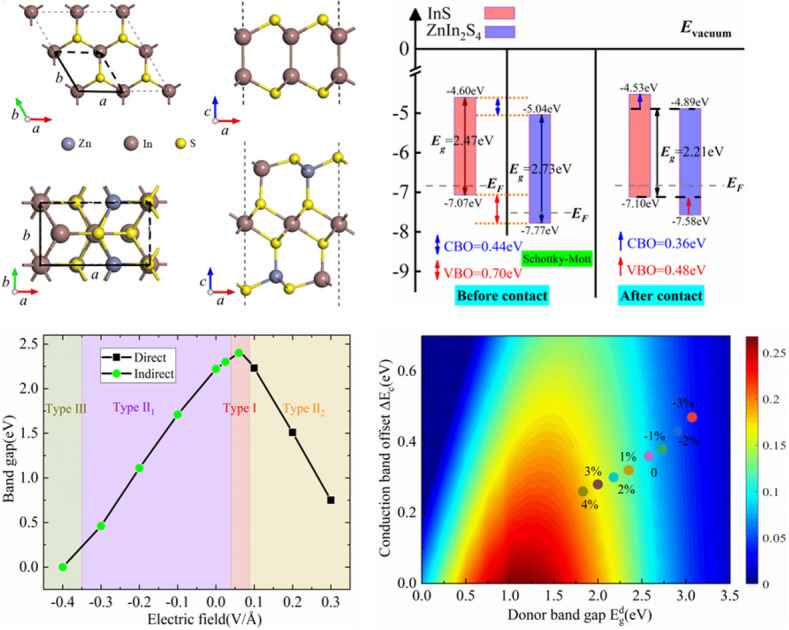
1. Introduction
Nowadays, in the face of increasing global energy shortages and environmental pollution, finding new green energy sources to replace traditional fuels has become a pressing issue, including solar energy, ocean energy, wind energy, biomass energy, and so on.1 Solar cells made of materials with specific photovoltaic properties can directly convert solar energy into electricity, which has become the main idea of the next generation of green power generation.2 Power conversion efficiency (PCE) is a metric that quantifies the efficiency with which a solar cell converts incident solar energy into useable electrical power. To enhance the PCE of solar cells, we can either employ high-quality photovoltaic materials (Si, CdSe, GaSe, and perovskite materials) with a wide spectral absorption range3,4 or create a heterojunction using two different semiconductor materials to increase the efficiency of the separation of photogenerated electrons and holes and to prolong the life time of the carriers.5,6 As we know, heterostructures can integrate the advantages of their individual constituent materials to overcome limitations, further enhancing their existing properties and expanding their applications.3,4,7–11 Heterostructures with type-II band alignment are commonly utilized in photocatalytic water splitting and photovoltaic devices.12,13
Since the emergence of graphene,14 two-dimensional (2D) materials and their heterostructures have garnered considerable attention owing to their unique physical properties and applications in novel optoelectronic devices.3,5,6,15–20 In recent years, solar cells constructed with 2D semiconductors heterostructures have received extensive theoretical and experimental research.6,20–22 Using polymer stacking and chemical vapor deposition (CVD), a graphene/WS2 heterostructure,23 WSe2/MoS2 heterostructure,24 WSe2/MoSe2 heterostructure,25 and p-Si/MoS2 heterostructure26 have been successfully prepared and exhibited a photoelectric conversion efficiency ranging from 0.12% to 5.23%. Furthermore, 2D GaX/SnS2 (X = S or Se), GaS/SnS2, Janus Ga2SeTe/InS, and SbI3/BiI3 heterostructures have been theoretically proposed for solar cells with a considerable PCE.4,6,27 Under atom doping, compressive strain, or an electric field, their PCE can reach up to 16.47%, 23.2%, and 21.63%, respectively.
Recently, a new family of 2D binary semiconductors, metal monochalcogenides MX (M = Ga, In; X = S, Se, Te), have garnered considerable interest because of their excellent physicochemical properties.28,29 The monolayer MX can be synthesized through mechanical exfoliation methods30,31 and vapor phase transport approach.32,33 MX monolayers have an indirect bandgap between 2.0 eV and 4.0 eV, and their band structure and optical absorption spectrum can be effectively modulated by layer thickness34,35 and nanofabrication.36 The InS monolayer and its heterostructure InS/InSe have been widely studied, possessing a PCE of 13.7%.37 Besides the binary metal monochalcogenides MX, the ternary metal chalcogenide semiconductor ZnIn2X4 (X = S, Se, Te) has also garnered significant interest owing to its excellent light absorption performance, and remarkable thermal and chemical stability.38,39 ZnIn2S4 nanosheets have now been synthesized and used for efficient photocatalytic hydrogen evolution, solar-powered CO2 conversion and hydrogen evolution reactions.40,41 In addition, many ZnIn2X4-based heterostructures have been fabricated and proposed for photodetectors, high-efficiency solar cells, and photocatalytic hydrogen evolution, such as O-SnS/I-ZnIn2S4,42 ZnIn2S4/ZnIn2Se4(ZnIn2Se4/ZnIn2Te4),43 and ZnIn2S4/SnSe2.44 Considering this, one intriguing question is whether the InS/ZnIn2S4 heterostructure could exhibit better electronic and optical properties, potentially leading to improved photovoltaic performance.
In this paper, firstly, we theoretically design the InS/ZnIn2S4 heterostructure and present a detailed study of its electronic and optical properties, including electronic structure, band alignment, optical absorption coefficients and PCE. It is found that the InS/ZnIn2S4 heterostructure possesses an indirect bandgap of 2.21 eV, a type-II1 band alignment, a large optical absorption coefficient, and a significant PCE of 10.86%. Next, the effects of an external field (electrical field and strain) on the band alignment and PCE of the InS/ZnIn2S4 heterostructure are also investigated. The band alignment transitions from type-II1 to type-I, type-II2 or type-III under an external electrical field, while it always stays in type-II1 under a biaxial strain. The PCE will increase to 12.19% at an external electric field of 0.2 V Å−1, and to 20.80% at a tensile strain of ε = 4%.
2. Methods
All calculations are carried out using the Vienna Ab initio Simulation Package (VASP),45,46 employing density functional theory (DFT). The exchange-correlation effect are treated with the generalized gradient approximation (GGA) of the Perdew–Burke–Ernzerhof (PBE) functional,47 within the projector augmented wave (PAW) framework.48,49 A plane wave cutoff energy of 450 eV is used. Geometric relaxation is performed until the residual force on each atom is below 0.01 eV Å−1. The Brillouin zone integration was sampled using 10 × 10 × 1 k-point meshes generated by the Monkhorst–Pack scheme.50 The electronic structure is also calculated using the Heyd–Scuseria–Ernzerhorf (HSE06) hybrid functionals.51 van der Waals (vdW) interactions between layers in the heterostructure are accounted for using a DFT-D2 approach.52 To eliminate spurious periodic interactions, a vacuum layer of 15 Å was introduced along the direction perpendicular to the heterostructure.
The binding energy Eb is calculated to assess the energy stability of the InS/ZnIn2S4 heterostructure, which is defined as the following equation,Eb = EInS/ZnIn2S4 − EInS − EZnIn2S4where EInS/ZnIn2S4 denotes the total energy of the InS/ZnIn2S4 heterostructure, while EInS and EZnIn2S4 represent the total energies of the isolated InS and ZnIn2S4 monolayers, respectively.
Both the optical absorption coefficient α(ω) and PCE are also calculated to quantitatively analyze the optical properties of the InS/ZnIn2S4 heterostructure. The α(ω) is computed from the following equation,53 where ε2(ω) represents the imaginary part of the dielectric function, and ε1(ω) is the real part of the dielectric function, derived from ε2(ω) through the Kramers–Kronig transformation. The PCE is defined as follows,54
 where βFF, VOC, JSC, and Psolar represent the band-fill factor, maximum open-circuit voltage, short-circuit current, and sum of the AM1.5 incident solar irradiation, respectively. βFF is typically assigned a value of 0.65,54VOC = Edg − ΔEc − 0.3, and
  . In addition, Edg, ΔEc, P(hω), and hω represent the donor layer's bandgap, conduction band offset (CBO) of the heterostructure, AM1.5 solar energy flux, and photon energy, respectively.
The carrier mobility for the InS/ZnIn2S4 van der Waals (vdW) heterostructure can be approximated using the deformation potential model, which is expressed as,55,56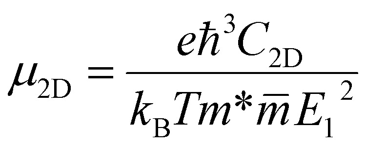 where e is the electron's charge, h is the reduced Planck constant, C2D is the elastic modulus, kB is the Boltzmann constant, T is the temperature set to 300 K,
 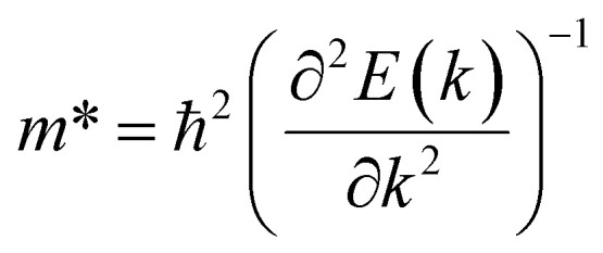 is the carrier effective mass,
 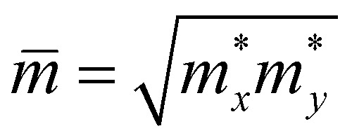 is the average carrier effective mass, and
 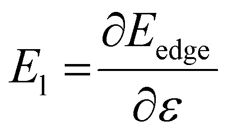 is the deformation potential constant, where Eedge represents the band edge energy of the electrons and holes produced by the infinitesimal uniaxial strain ε, along the armchair and zigzag directions.
3. Results and discussion
The crystal structure and band structure of the isolated InS and ZnIn2S4 monolayers are displayed in Fig. S1.† The monolayer InS has a hexagonal lattice and four atomic-layer structure with a unit cell containing two In and two S atoms. The lattice constants of InS are aInS = bInS = 3.93 Å. The valence band maximum (VBM) is along the Γ–M line, while the conduction band minimum (CBM) is at Γ point, indicating that InS is an indirect band gap semiconductor. The band gap of InS is calculated to be 1.66 eV under the PBE functional level and 2.47 eV under the HSE06 functional level, consistent with previous reports.28 The monolayer ZnIn2S4 forms a rectangular lattice and seven atomic-layer structure with a unit cell containing two Zn, four In and eight S atoms. The lattice constants of ZnIn2S4 are aZnIn2s4 = 6.78 Å and bZnIn2s4 = 3.93 Å. The CBM and VBM are both situated at the Γ point, which means that it is a direct band gap semiconductor. The calculated band gap of ZnIn2S4 is 1.79 eV under the PBE functional level and 2.73 eV under the HSE06 functional level, consistent with a previous study.39 Moreover, for both InS and ZnIn2S4 monolayers, the HSE06 functional only increased the bandgap and did not change the general shape of the band structure. For all subsequent calculations, we only use the HSE06 functional.
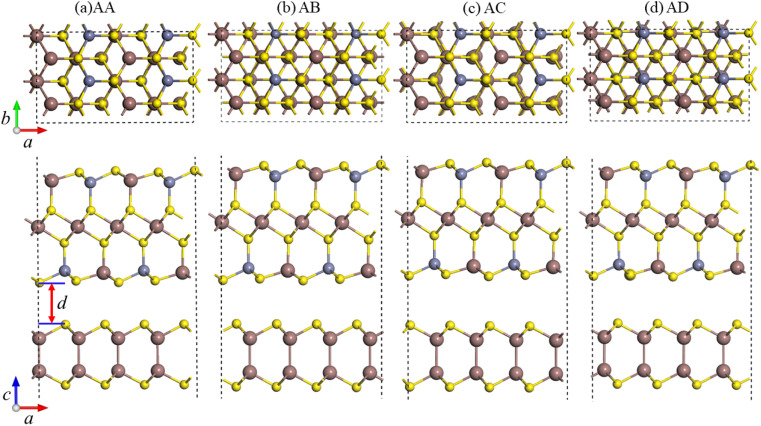
To construct a two-dimensional InS/ZnIn2S4 heterostructure with a small lattice mismatch,57,58 a √3 × 1 supercell of the isolated InS monolayer and a unit cell of ZnIn2S4 monolayer are selected. The lattice mismatch is determined using the following formula  for the x direction and [(bZnIn2S4 − bInS)/bZnIn2S4] × 100% for the y direction, and the corresponding mismatch values are 0.14% and 0%, respectively. Then, to determine the energetically favorable structure of the InS/ZnIn2S4 heterostructures, we consider four representative heterostructures formed with different stacking configuration, specifically AA, AB, AC and AD, as shown in Fig. 1. The equilibrium structural parameters (lattice parameters a and b, interlayer distance d) and binding energy Eb of the four configurations of the InS/ZnIn2S4 heterostructures are listed in Table S1.† These four heterostructures have nearly identical lattice parameters of a ≈ 6.80 Å and b ≈ 3.93 Å, which closely resemble the dimensions of the unit cell of the isolated ZnIn2S4 (or √3 × 1 supercell of the isolated InS monolayer). The calculated interlayer distances d of the InS/ZnIn2S4 heterostructures with AA, AB, AC, and AD stacking are 3.71, 3.77, 4.19, and 4.03 Å, respectively. All four stacking configurations are energetically stable, as their binding energies Eb are negative.59 The InS/ZnIn2S4 heterostructure with AA stacking is the most energetically favorable, since it has the smallest binding energy. To evaluate the dynamic and thermal stability of the InS/ZnIn2S4 heterostructure, the phonon spectrum was obtained and molecular dynamics simulations are also performed. The phonon dispersion does not have an imaginary mode, as shown in Fig. S4(a),† which indicates that the heterostructure is dynamically stable. The fluctuations of the total energy of the InS/ZnIn2S4 heterostructure at room temperature (300 K) as a function of time is depicted in Fig. S4(b).† The results suggest that the heterostructure is thermally stable at room temperature, since the fluctuation of the total energies is small. In addition, the AA stacking configuration has the smallest interlayer distance d. In subsequent studies, we mainly focus on the AA stacking configuration.
Fig. 1. Top and side views of the four possible stacking configurations of the InS/ZnIn2S4 heterostructures: (a) AA, (b) AB, (c) AC, and (d) AD. d represents the interlayer distance.
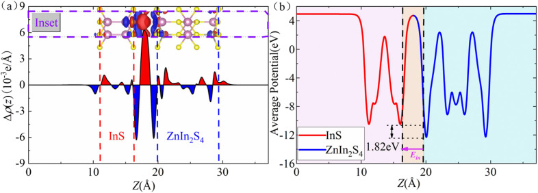
Fig. 2(a) shows the charge density difference Δρ, defined as Δρ = ρInS/ZnIn2S4 − ρInS − ρZnIn2S4. Here, ρZnIn2S4, ρInS, and ρZnIn2S4 represent the charge density of the InS/ZnIn2S4 heterostructure, isolated InS, and isolated ZnIn2S4, respectively. The planar-averaged charge density difference Δρ(z), defined as  , is also displayed in Fig. 2(a). Here, Axy represents the surface area of the InS/ZnIn2S4 heterostructures.60 The curves of Δρ(z) were oscillated, and the amplitude of the oscillations experiences a notable surge in proximity to the interface, indicating that charge transfer and rearrangement occur within the interfacial region of the InS/ZnIn2S4 heterostructure. In addition, from the three-dimensional charge density difference Δρ, we find that the electrons primarily accumulate in the vdW gap between the InS and ZnIn2S4 layers, while the electron-deficient regions predominantly occur around the interface S atoms of both InS layer and ZnIn2S4 layer. Furthermore, Bader charge analysis indicates that there is a charge transfer of about 0.004e that occurs from the ZnIn2S4 layer to the InS layer. This can induce a weak effective built-in electric field (Ein) at the interface that is directed from the ZnIn2S4 layer toward the InS layer,61,62 as shown by the pink arrow in Fig. 2(b). Fig. 2(b) shows the planar-averaged electrostatic potential V profiles along the z-axis, from which Ein can be inferred based on the potential drop ΔV at the interface of the heterostructure. This electric field plays a crucial role in facilitating the separation of photoinduced electron–hole pairs, thereby prolonging the lifetimes of carriers in the heterostructure. In addition, we calculated the carrier mobility of the InS/ZnIn2S4 heterostructure. Table S4† lists the calculated carrier effective mass, the deformation potential constant, and the corresponding carrier mobilities along the zigzag and armchair directions of the InS/ZnIn2S4 heterostructure. It can be seen that the hole mobility of the InS/ZnIn2S4 heterostructure is higher than that of electrons, and the hole mobility along the armchair direction reaches 6118.01 cm2 V−1 s−1. The high carrier mobility characteristic gives it significant advantages in photovoltaic applications.
Fig. 2. (a) The planar-averaged charge density difference Δρ(z) of the InS/ZnIn2S4 heterostructure (inset: three-dimensional charge density difference Δρ). Red regions indicate electron accumulation, while blue regions signify electron depletion. (b) The planar-averaged electrostatic potential of the InS/ZnIn2S4 heterostructure along the z-axis. The potential drop ΔV at the interface is 1.82 eV. The pink arrow indicates the direction of the built-in electric field.
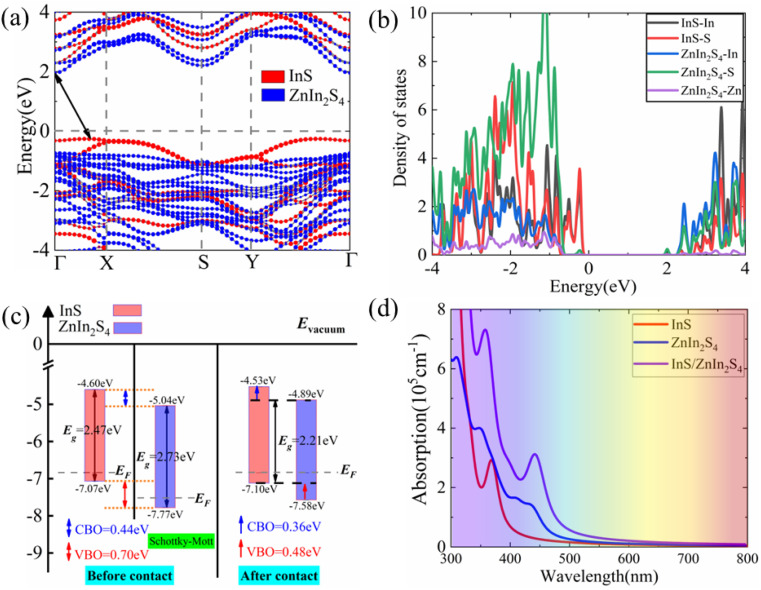
Fig. 3(a)–(c) present the projected band structure, projected density of states (DOS) and band alignment of the InS/ZnIn2S4 heterostructure. The heterostructure is a semiconductor with an indirect bandgap of 2.21 eV, where the CBM is at Γ point, while the VBM is along the Γ–X line, which is smaller than both InS (2.47 eV) and ZnIn2S4 (2.73 eV). From the projected band structure and projected DOS, we find that the CBM is derived from the ZnIn2S4 layer and predominantly contributed by S and In atoms in the ZnIn2S4 layer, while the VBM is derived from the InS layer and primarily dominated by S atoms in the InS layer. Interestingly, we find that the InS/ZnIn2S4 heterostructure exhibits type-II band alignment, in which the CBM and VBM of the ZnIn2S4 layer are lower than those of the InS layer, also denoted as type-II1 band alignment, as illustrated in Fig. 3(c). Moreover, when the external electric field is greater than 0.1 V Å−1, the CBM and VBM of the ZnIn2S4 layer will be higher than those of the InS layer, resulting in another type-II alignment that is different from type-II1, defined as type-II2, as shown in Fig. 4(a). In addition, the calculated conduction band offset (CBO) and valence band offset (VBO) are 0.36 eV and 0.48 eV, respectively, both of which are smaller than those calculated using the Schottky–Mott model.63 In the ideal Schottky–Mott limit, there is no interaction between the InS and ZnIn2S4 layer, the CBO and VBO are 0.44 eV and 0.70 eV, respectively. The type-II band alignment will significantly improve the efficiency of the separating photoinduced electron–hole pairs at the InS/ZnIn2S4 heterostructure's interface, in which the InS layer can act as an electron donor, while the ZnIn2S4 layer acts as an electron acceptors. The absorption spectra of the InS/ZnIn2S4 heterostructure, as well as isolated InS and ZnIn2S4 monolayers, are displayed (https://www.wordhippo.com/what-is/another-word-for/display.html) in Fig. 3(d). Compared with InS and ZnIn2S4 monolayer, the InS/ZnIn2S4 heterostructure demonstrates improved light absorption in the visible short-wavelength region (approximately 300–500 nm), which is mainly due to the bandgap narrowing after the formation of the heterostructure.
Fig. 3. The projected band structure (a), projected DOS (b), band alignment (c), and absorption spectra (d) of the InS/ZnIn2S4 heterostructure using the vacuum energy levels as a common energy reference. Eg and EF denote the energies of the bandgap and Fermi energy levels, respectively. The CBO and VBO are represented by blue and red arrows, respectively.
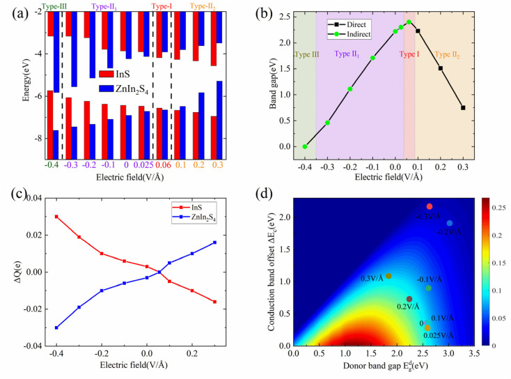
Fig. 4. The band alignments (a), band gaps (b), and charge transfer (c) of the InS/ZnIn2S4 heterostructure under different electric fields. (d) The η of the InS/ZnIn2S4 heterostructure as a function of ΔEc and Edg under different electric fields.
Considering that the InS/ZnIn2S4 heterostructure possesses Ein, type-II band alignment, and significant absorption coefficients in the ultraviolet and visible light bands, it may exhibit high-efficiency performance in solar cells. To study the η of the InS/ZnIn2S4 heterostructure, we calculated the donor's bandgap (Edg), the ratio of the short-circuit current density to the AM1.5 solar flux (Jsc/Psolar), the conduction band offset (ΔEc), open circuit voltage (Voc), and η, as listed in Tables S2 and S3.† The Jsc/Psolar and Voc of the InS/ZnIn2S4 heterostructure are 0.087 and 1.91 V, respectively, resulting in a η of 10.80%.
In practical applications, applying an external electric field (gate voltage) can modulate the characteristics of a given material. Here, we study the impact of a vertical electric field on the electronic band structure and band alignment of the InS/ZnIn2S4 heterostructure. The projected band structures and band alignments of the InS/ZnIn2S4 heterostructure under vertical electric fields (E⊥) ranging from −0.4 to 0.3 V Å−1 are presented in Fig. S2† and 4(a), where the direction of the positive electric field is set to point from the InS layer to ZnIn2S4 layer. We also calculate the interlayer charge transfer (ΔQ) of the InS/ZnIn2S4 heterostructure under different E⊥, as depicted in Fig. 4(c).
Under the positive E⊥, the direction of Ein is opposite to that of E⊥, and the band edge position of ZnIn2S4 layer will shifts upward with respect to that of the InS layer. When 0 < E⊥ < 0.05 V Å−1, the direction of the total electrical field (Et) is the same as Ein, and there is a charge transfer from ZnIn2S4 to InS. The CBM and VBM of the ZnIn2S4 layer are both lower than those of the InS layer, and the heterostructure maintains a type-II1 band alignment. With increasing E⊥, the amount of ΔQ will decrease, and the CBO and VBO will both decrease. When 0.05 < E⊥ < 0.09 V Å−1, the direction of Et is same as that for E⊥, and there will be a charge transfer from InS to ZnIn2S4. The CBM of the ZnIn2S4 layer is higher than that of the InS layer, and the VBM of the ZnIn2S4 layer is lower than that of the InS layer. The heterostructure thus changes into a straddling type-I band alignment. At this point, both the CBM and VBM of the InS/ZnIn2S4 heterostructure are contributed by the InS layer, making it easier to form electron hole pairs during electron transitions. This makes it potentially applicable in optoelectronic devices such as light-emitting diodes and lasers. With the increase of E⊥, the amount of ΔQ will increase, the CBO will increase, and VBO will further decrease. When 0.09 < E⊥ < 0.3V Å−1, the direction of Et is also the same as that of E⊥, and there will be a charge transfer from InS to ZnIn2S4. The CBM and VBM of the ZnIn2S4 layer both become higher than those of the InS layer, causing the heterostructure to transition into type-II2 band alignment. With the increasing of E⊥, the amount of ΔQ will increase, and the CBO and VBO will both increase.
Under a negative E⊥, the Ein and E⊥ have the same direction, so the direction of Et consistently matches the Ein. There is a charge transfer (ΔQ) from ZnIn2S4 to InS. The band edge position of the ZnIn2S4 layer moves downwards relative to that of the InS layer. With the increasing of the E⊥, the ΔQ will increase gradually, and the CBO and VBO will both increase gradually. When −0.35 < E⊥ < 0.0V Å−1, the CBM and VBM of the ZnIn2S4 layer both become lower than those of the InS layer, and the heterostructure can maintain a type-II1 band alignment. When E⊥ ≥ 0.35 V Å−1, the VBM of InS becomes higher than the VBM and CBM of ZnIn2S4, and the band alignment of the heterostructure becomes type-III.
Moreover, the band gap size and type of the InS/ZnIn2S4 heterostructure are largely modulated by the electrical field, as displayed in Fig. 4(b). Under a positive E⊥, as the E⊥ is increasing, the band gap of the InS/ZnIn2S4 heterostructure will firstly increase and then decrease. Under a negative E⊥, the band gap of the InS/ZnIn2S4 heterostructure will monotonically decrease with increasing E⊥. The heterostructure can also change to a direct bandgap semiconductor when 0.09 < E⊥ < 0.3V Å−1.
Next, we attempt to explore the η of the InS/ZnIn2S4 heterostructure under different electric fields. As we know, to obtain a high η, a moderate Edg is desirable. This is because the Voc will be enlarged and the Jsc/Psolar will be reduced by increasing Edg. Secondly, the ΔEc is as low as possible to reduce the energy loss and obtain a high Voc. The calculated Edg, Jsc/Psolar, ΔEc, Voc, and η of the heterostructure with type-II alignment under different E⊥ are listed in Table S2.† When E⊥ < 0, both Edg and ΔEc will be enlarged, which result in Jsc/Psolar and Voc both being reduced, so the η of the heterostructure becomes lower. When E⊥ > 0, Edg will be enlarged and ΔEc will be reduced. Subsequently, Edg will be reduced and ΔEc will be enlarged, which result in Jsc/Psolar and Voc exhibiting different varying trends. Hence, the η also exhibits a nonmonotonic variation. For E⊥ = 0.2 V Å−1 and 0.3 V Å−1, the values of Edg are 2.24 eV and 1.84 eV, respectively, which may theoretically result in large η. However, when E⊥ > 0.2 V Å−1, the ΔEc dramatically increases, reaching as high as 1.09 eV at E⊥ = 0.3 V Å−1. This results in a significant decrease in Voc. The η can be increased up to 12.19% at E⊥ = 0.2 V Å−1, as shown Fig. 4(d) and Table S2.†
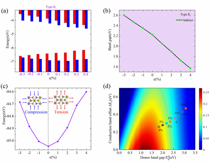
Strain engineering can also modulate the electronic properties and η of the semiconductor materials and their heterostructures.17,19 Firstly, we attempt to examine the influence of biaxial strain (ε) on the electronic properties of the InS/ZnIn2S4 heterostructure. The biaxial strain (ε) is given by ε = (a − a0)/a0, where a and a0 represent the lattice constants of the strained and unstrained heterostructure, respectively. The strength of ε ranging from −3% to 4% is considered, where a negative (positive) sign refers to compressive (tensile) strain. An increase in total energy is observed by applying a tensile or compressive strain, and the change in total energy is fitted to a quadratic curve, as depicted in Fig. 5(c). The electronic structure and band offset of the InS/ZnIn2S4 heterostructure under different ε are given in Fig. S3† and 5.
Fig. 5. The band alignments (a), band gaps (b), and the total energy (c) of the InS/ZnIn2S4 heterostructure under different biaxial strains. (d) The η of the InS/ZnIn2S4 heterostructure as a function of ΔEc and Edg under different biaxial strains.
Under tensile strain, as the ε increases, the VBM of InS moves up and the CBM of ZnIn2S4 moves down, and the band gap of the InS/ZnIn2S4 heterostructure decreases linearly. At ε = 4%, the bandgap decreases from 2.21 eV to 1.57 eV. Under compressive strain, as the ε increases, the VBM of InS moves down and the CBM of ZnIn2S4 moves up, and the band gap of InS/ZnIn2S4 heterostructure increase linearly. At ε = −3%, the bandgap of the InS/ZnIn2S4 heterostructure is increased from 2.21 eV to 2.60 eV. Moreover, for −3% < ε < 4%, the InS/ZnIn2S4 heterostructure always maintains a type-II1 band alignment, along with an indirect band gap. The InS/ZnIn2S4 heterostructure can maintain a stable Type II alignment under biaxial strain ranging from −3% to 4%, suggesting its potential as a stable candidate material for solar cells.
Next, we calculate the Edg, Jsc/Psolar, ΔEc, Voc, and η of the InS/ZnIn2S4 heterostructure under different ε, as summarized in Table S3.† Under tensive strain, Edg and ΔEc decrease linearly with increasing strain, which result in the Jsc/Psolar being enlarged and the Voc being reduced. Furthermore, the η values of the InS/ZnIn2S4 heterostructure are enlarged. When ε = 4%, a high η of 20.80% was achieved, as displayed in Fig. 5(d) and Table S3.† Under compressive strain, Edg and ΔEc also increase linearly with increasing strain, which result in the Jsc/Psolar being reduced and the Voc being increased. However, the η values of the InS/ZnIn2S4 heterostructure are significantly reduced. When ε = −3%, the η is reduced to 4.18%, as shown in Fig. 5(d) and Table S3.† Therefore, biaxial strain modulation could be an effective approach to increase the η.64
4. Conclusions
In summary, we propose the two-dimensional InS/ZnIn2S4 heterostructure, and examine its electronic and optical characteristics using first principles calculations, focusing particularly on the band alignment and PCE. The AA stacking configuration is the most energetically favorable, possessing an indirect band gap of 2.21 eV and a large optical absorption coefficient in the short-wavelength visible region, along with a type-II1 band alignment. Additionally, a significant η of 10.86% has been achieved. The band alignment and η of the InS/ZnIn2S4 heterostructure are largely modulated by applying an external electrical field or biaxial strain. The transformation of the band alignment from type-II1 to type-I or type-II2 can be induced by an external electric field, resulting in a further increase in η up to 12.19% at a positive E⊥ = 0.2 V Å−1. The type-II1 band alignment remains stable within a critical biaxial strain of 4%, and a high η of 20.80% is achieved under a tensile strain of ε = 4%. This work is expected to provide new inspiration for improving solar cells with high PCE based on 2D InS/ZnIn2S4 heterostructures.
Data availability
The data supporting this study have been included within the article and its ESI.† Additional data will be made available on reasonable request.
Author contributions
Hui-Ying Liu: data curation (equal); formal analysis (equal); investigation (equal); writing – original draft (equal). Heng-Fu Lin: conceptualization (equal); formal analysis (equal); investigation (equal); supervision (equal); writing – review & editing (equal). Lu-Ya Xu: data curation (equal); formal analysis (equal); Ting-Ping Hou: conceptualization (equal); formal analysis (equal); investigation (equal); supervision (equal); writing – review & editing (equal). Nan-shu Liu: conceptualization (equal); formal analysis (equal); investigation (equal); supervision (equal); writing – review & editing (equal).
Conflicts of interest
The authors have no conflicts of interest.
Supplementary Material
Acknowledgments
This work was supported by the National Natural Science Foundation of China (12374191, 12204534), Fundamental Research Funds for the Central Universities (SWU-KQ24053) and Knowledge Innovation Program of Wuhan-Shuguang Project (No. 2023010201020404). This work was also supported by the computing time award at the High Performance Computing Center of Wuhan University of Science and Technology.
Electronic supplementary information (ESI) available. See DOI: https://doi.org/10.1039/d4ra06901c
References
- Cui Y. Yao H. Hong L. Zhang T. Tang Y. Lin B. Xian K. Gao B. An C. Bi P. Ma W. Hou J. Natl. Sci. Rev. 2020;7:1239–1246. doi: 10.1093/nsr/nwz200. [DOI] [PMC free article] [PubMed] [Google Scholar]
- Cui Y. Yao H. Zhang J. Xian K. Zhang T. Hong L. Wang Y. Xu Y. Ma K. An C. He C. Wei Z. Gao F. Hou J. Adv. Mater. 2020;32:1908205. doi: 10.1002/adma.201908205. [DOI] [PubMed] [Google Scholar]
- Yu Z. Sun L. Adv. Energy Mater. 2015;5:1500213. [Google Scholar]
- Wu H. Yang K. Si Y. Huang W. Hu W. Huang G. Phys. Status Solidi RRL. 2019;13:1800565. [Google Scholar]
- Chen Y. Ye P. Zhu Z.-G. Wang X. Yang L. Xu X. Wu X. Dong T. Zhang H. Hou J. Liu F. Huang H. Adv. Mater. 2017;29:1603154. doi: 10.1002/adma.201603154. [DOI] [PubMed] [Google Scholar]
- Liang K. Huang T. Yang K. Si Y. Wu H.-Y. Lian J.-C. Huang W.-Q. Hu W.-Y. Huang G.-F. Phys. Rev. Appl. 2021;16:054043. [Google Scholar]
- Yan R. Fathipour S. Han Y. Song B. Xiao S. Li M. Ma N. Protasenko V. Muller D. A. Jena D. Xing H. G. Nano Lett. 2015;15:5791–5798. doi: 10.1021/acs.nanolett.5b01792. [DOI] [PubMed] [Google Scholar]
- Datta K. Khosru Q. D. J. Comput. Electron. 2017;16:228–239. [Google Scholar]
- Zhang J.-R. Deng X.-Z. Gao B. Chen L. Au C.-T. Li K. Yin S.-F. Cai M.-Q. Catal. Sci. Technol. 2019;9:4659–4667. [Google Scholar]
- Bellus M. Z. Li M. Lane S. D. Ceballos F. Cui Q. Zeng X. C. Zhao H. Nanoscale Horiz. 2016;2:31–36. doi: 10.1039/c6nh00144k. [DOI] [PubMed] [Google Scholar]
- Williams K. R. Diroll B. T. Watkins N. E. Rui X. Brumberg A. Klie R. F. Schaller R. D. J. Am. Chem. Soc. 2019;141:5092–5096. doi: 10.1021/jacs.8b13794. [DOI] [PubMed] [Google Scholar]
- Wang Y. Wang Q. Zhan X. Wang F. Safdar M. He J. Nanoscale. 2013;5:8326–8339. doi: 10.1039/c3nr01577g. [DOI] [PubMed] [Google Scholar]
- Almadori Y. Bendiab N. Grévin B. ACS Appl. Mater. Interfaces. 2018;10:1363–1373. doi: 10.1021/acsami.7b14616. [DOI] [PubMed] [Google Scholar]
- Novoselov K. S. Geim A. K. Morozov S. V. Jiang D. Zhang Y. Dubonos S. V. Grigorieva I. V. Firsov A. A. Science. 2004;306:666–669. doi: 10.1126/science.1102896. [DOI] [PubMed] [Google Scholar]
- Lemme M. C. Akinwande D. Huyghebaert C. Stampfer C. Nat. Commun. 2022;13:1392. doi: 10.1038/s41467-022-29001-4. [DOI] [PMC free article] [PubMed] [Google Scholar]
- Chaves A. Azadani J. G. Alsalman H. Da Costa D. R. Frisenda R. Chaves A. J. Song S. H. Kim Y. D. He D. Zhou J. Castellanos-Gomez A. Peeters F. M. Liu Z. Hinkle C. L. Oh S.-H. Ye P. D. Koester S. J. Lee Y. H. Avouris Ph. Wang X. Low T. npj 2D Mater. Appl. 2020;4:29. [Google Scholar]
- Cheng Z. Cao R. Wei K. Yao Y. Liu X. Kang J. Dong J. Shi Z. Zhang H. Zhang X. Adv. Sci. 2021;8:2003834. doi: 10.1002/advs.202003834. [DOI] [PMC free article] [PubMed] [Google Scholar]
- Sheng C. Dong X. Zhu Y. Wang X. Chen X. Xia Y. Xu Z. Zhou P. Wan J. Bao W. Adv. Funct. Mater. 2023;33:2304778. [Google Scholar]
- Novoselov K. S. Mishchenko A. Carvalho A. Castro Neto A. H. Science. 2016;353:aac9439. doi: 10.1126/science.aac9439. [DOI] [PubMed] [Google Scholar]
- Pham P. V. Bodepudi S. C. Shehzad K. Liu Y. Xu Y. Yu B. Duan X. Chem. Rev. 2022;122:6514–6613. doi: 10.1021/acs.chemrev.1c00735. [DOI] [PubMed] [Google Scholar]
- Yu Y. Hu S. Su L. Huang L. Liu Y. Jin Z. Purezky A. A. Geohegan D. B. Kim K. W. Zhang Y. Cao L. Nano Lett. 2015;15:486–491. doi: 10.1021/nl5038177. [DOI] [PubMed] [Google Scholar]
- Li X. Tao L. Chen Z. Fang H. Li X. Wang X. Xu J.-B. Zhu H. Appl. Phys. Rev. 2017;4:021306. [Google Scholar]
- Shanmugam M. Jacobs-Gedrim R. Song E. S. Yu B. Nanoscale. 2014;6:12682–12689. doi: 10.1039/c4nr03334e. [DOI] [PubMed] [Google Scholar]
- Furchi M. M. Pospischil A. Libisch F. Burgdörfer J. Mueller T. Nano Lett. 2014;14:4785–4791. doi: 10.1021/nl501962c. [DOI] [PMC free article] [PubMed] [Google Scholar]
- Gong Y. Lei S. Ye G. Li B. He Y. Keyshar K. Zhang X. Wang Q. Lou J. Liu Z. Vajtai R. Zhou W. Ajayan P. M. Nano Lett. 2015;15:6135–6141. doi: 10.1021/acs.nanolett.5b02423. [DOI] [PubMed] [Google Scholar]
- Tsai M.-L. Su S.-H. Chang J.-K. Tsai D.-S. Chen C.-H. Wu C.-I. Li L.-J. Chen L.-J. He J.-H. ACS Nano. 2014;8:8317–8322. doi: 10.1021/nn502776h. [DOI] [PubMed] [Google Scholar]
- Lai K. Li H. Xu Y.-K. Zhang W.-B. Dai J. Phys. Chem. Chem. Phys. 2019;21:2619–2627. doi: 10.1039/c8cp07298a. [DOI] [PubMed] [Google Scholar]
- Sun H. Wang Z. Wang Y. AIP Adv. 2017;7:095120. [Google Scholar]
- Lin H.-F. Liu H.-Y. Wang M. Wang S.-S. Hou T.-P. Wu K.-M. Phys. Chem. Chem. Phys. 2022;24:4425–4436. doi: 10.1039/d1cp04413c. [DOI] [PubMed] [Google Scholar]
- Wang Z. Xu K. Li Y. Zhan X. Safdar M. Wang Q. Wang F. He J. ACS Nano. 2014;8:4859–4865. doi: 10.1021/nn500782n. [DOI] [PubMed] [Google Scholar]
- Hu P. Wen Z. Wang L. Tan P. Xiao K. ACS Nano. 2012;6:5988–5994. doi: 10.1021/nn300889c. [DOI] [PubMed] [Google Scholar]
- Xu K. Yin L. Huang Y. Shifa T. A. Chu J. Wang F. Cheng R. Wang Z. He J. Nanoscale. 2016;8:16802–16818. doi: 10.1039/c6nr05976g. [DOI] [PubMed] [Google Scholar]
- Demirci S. Avazlı N. Durgun E. Cahangirov S. Phys. Rev. B. 2017;95:115409. [Google Scholar]
- Mudd G. W. Svatek S. A. Ren T. Patanè A. Makarovsky O. Eaves L. Beton P. H. Kovalyuk Z. D. Lashkarev G. V. Kudrynskyi Z. R. Dmitriev A. I. Adv. Mater. 2013;25:5714–5718. doi: 10.1002/adma.201302616. [DOI] [PMC free article] [PubMed] [Google Scholar]
- Lei S. Ge L. Najmaei S. George A. Kappera R. Lou J. Chhowalla M. Yamaguchi H. Gupta G. Vajtai R. Mohite A. D. Ajayan P. M. ACS Nano. 2014;8:1263–1272. doi: 10.1021/nn405036u. [DOI] [PubMed] [Google Scholar]
- Brotons-Gisbert M. Andres-Penares D. Suh J. Hidalgo F. Abargues R. Rodríguez-Cantó P. J. Segura A. Cros A. Tobias G. Canadell E. Ordejón P. Wu J. Martínez-Pastor J. P. Sánchez-Royo J. F. Nano Lett. 2016;16:3221–3229. doi: 10.1021/acs.nanolett.6b00689. [DOI] [PubMed] [Google Scholar]
- Rawat A. Ahammed R. Jena D. N. Mohanta M. K. De Sarkar A. J. Phys. Chem. C. 2019;123:12666–12675. [Google Scholar]
- Luo R.-B. Liu Q.-J. Fan D.-H. Liu Z.-T. Appl. Surf. Sci. 2022;605:154739. [Google Scholar]
- Mohebpour M. A. Mortazavi B. Rabczuk T. Zhuang X. Shapeev A. V. Tagani M. B. Phys. Rev. B. 2022;105:134108. [Google Scholar]
- Zhang S. Zhang Z. Si Y. Li B. Deng F. Yang L. Liu X. Dai W. Luo S. ACS Nano. 2021;15:15238–15248. doi: 10.1021/acsnano.1c05834. [DOI] [PubMed] [Google Scholar]
- Long L. Lv G. Pan F. Li Z. Zhu H. Wang D. J. Phys. Chem. C. 2023;127:24077–24087. [Google Scholar]
- Ye Q. Xu D. Cai B. Lu J. Yi H. Ma C. Zheng Z. Yao J. Ouyang G. Yang G. Mater. Horiz. 2022;9:2364–2375. doi: 10.1039/d2mh00612j. [DOI] [PubMed] [Google Scholar]
- Liang Z. Liu Y.-Z. Gong Z.-T. Li J.-Y. Yao Y.-S. Tang Z.-K. Wei X.-L. Dalton Trans. 2024;53:4729–4736. doi: 10.1039/d3dt04276f. [DOI] [PubMed] [Google Scholar]
- Wang X. Wang X. Shi T. Meng A. Wang L. Li S. Li G. Yu X. Li Z. Sol. RRL. 2023;7:2200881. [Google Scholar]
- Kresse G. Furthmüller J. Phys. Rev. B:Condens. Matter Mater. Phys. 1996;54:11169–11186. doi: 10.1103/physrevb.54.11169. [DOI] [PubMed] [Google Scholar]
- Kresse G. Furthmüller J. Comput. Mater. Sci. 1996;6:15–50. [Google Scholar]
- Perdew J. P. Burke K. Ernzerhof M. Phys. Rev. Lett. 1996;77:3865–3868. doi: 10.1103/PhysRevLett.77.3865. [DOI] [PubMed] [Google Scholar]
- Blöchl P. E. Phys. Rev. B:Condens. Matter Mater. Phys. 1994;50:17953–17979. doi: 10.1103/physrevb.50.17953. [DOI] [PubMed] [Google Scholar]
- Kresse G. Joubert D. Phys. Rev. B:Condens. Matter Mater. Phys. 1999;59:1758–1775. [Google Scholar]
- Monkhorst H. J. Pack J. D. Phys. Rev. B: Solid State. 1976;13:5188–5192. [Google Scholar]
- Paier J. Marsman M. Hummer K. Kresse G. Gerber I. C. Angyán J. G. J. Chem. Phys. 2006;124:154709. doi: 10.1063/1.2187006. [DOI] [PubMed] [Google Scholar]
- Grimme S. J. Comput. Chem. 2006;27:1787–1799. doi: 10.1002/jcc.20495. [DOI] [PubMed] [Google Scholar]
- Gajdoš M. Hummer K. Kresse G. Furthmüller J. Bechstedt F. Phys. Rev. B:Condens. Matter Mater. Phys. 2006;73:045112. [Google Scholar]
- Scharber M. C. Mühlbacher D. Koppe M. Denk P. Waldauf C. Heeger A. J. Brabec C. J. Adv. Mater. 2006;18:789–794. [Google Scholar]
- Bruzzone S. Fiori G. Appl. Phys. Lett. 2011;99:222108. [Google Scholar]
- Vu T. V. Nguyen C. V. Phuc H. V. Lavrentyev A. A. Khyzhun O. Y. Hieu N. V. Obeid M. M. Rai D. P. Tong H. D. Hieu N. N. Phys. Rev. B. 2021;103:085422. [Google Scholar]
- Shen T. Ren J.-C. Liu X. Li S. Liu W. J. Am. Chem. Soc. 2019;141:3110–3115. doi: 10.1021/jacs.8b12212. [DOI] [PubMed] [Google Scholar]
- Kibirev I. A. Matetskiy A. V. Zotov A. V. Saranin A. A. Appl. Phys. Lett. 2018;112:191602. [Google Scholar]
- Nguyen H. T. T. Obeid M. M. Bafekry A. Idrees M. Vu T. V. Phuc H. V. Hieu N. N. Hoa L. T. Amin B. Nguyen C. V. Phys. Rev. B. 2020;102:075414. [Google Scholar]
- Li Q. Chen K.-Q. Tang L.-M. Phys. Rev. Appl. 2020;13:014064. doi: 10.1103/physrevapplied.13.014020. [DOI] [PMC free article] [PubMed] [Google Scholar]
- Wang B.-J. Li X.-H. Zhao R. Cai X.-L. Yu W.-Y. Li W.-B. Liu Z.-S. Zhang L.-W. Ke S.-H. J. Mater. Chem. A. 2018;6:8923–8929. [Google Scholar]
- Ren K. Tang W. Sun M. Cai Y. Cheng Y. Zhang G. Nanoscale. 2020;12:17281–17289. doi: 10.1039/d0nr02286a. [DOI] [PubMed] [Google Scholar]
- Tung R. T. Appl. Phys. Lett. 2014;1:011304. [Google Scholar]
- Zhao J. Li Y. Yang G. Jiang K. Lin H. Ade H. Ma W. Yan H. Nat. Energy. 2016;1:1–7. [Google Scholar]
Associated Data
This section collects any data citations, data availability statements, or supplementary materials included in this article.
Supplementary Materials
Data Availability Statement
The data supporting this study have been included within the article and its ESI.† Additional data will be made available on reasonable request.


