Abstract
In many physical and biological systems the transition from an amorphous to ordered native structure involves complex energy landscapes, and understanding such transformations requires not only their thermodynamics but also the structural dynamics during the process. Here, we extend our 4D visualization method with electron imaging to include the study of irreversible processes with a single pulse in the same ultrafast electron microscope (UEM) as used before in the single-electron mode for the study of reversible processes. With this augmentation, we report on the transformation of amorphous to crystalline structure with silicon as an example. A single heating pulse was used to initiate crystallization from the amorphous phase while a single packet of electrons imaged selectively in space the transformation as the structure continuously changes with time. From the evolution of crystallinity in real time and the changes in morphology, for nanosecond and femtosecond pulse heating, we describe two types of processes, one that occurs at early time and involves a nondiffusive motion and another that takes place on a longer time scale. Similar mechanisms of two distinct time scales may perhaps be important in biomolecular folding.
Keywords: diffraction, imaging, structural dynamics, ultrafast electron microscopy
The transformation of amorphous structures, such as liquids or random-coiled proteins, into ordered structures involves complex dynamical processes that ultimately lead to the final native state. The mechanism is determined by the scales of time, length, and energy as they define the nature of the elementary steps involved. For example, an amorphous bulk liquid crystallizes depending on the degree of initial (nanoscale) nucleation, the time scale of heat diffusion, and the latent energy acquired. Similarly, for a protein, the funneling toward the native structure requires the balance of the entropic and enthalpic free energy contributions, as well as the “diffusion” through many energy barriers, possibly with nucleation on the path to the final state.
To observe such processes on the time-length scale of the phenomena, our method of choice has been 4D space–time visualization (ref. 1 and references therein, and ref. 2) developed in ultrafast electron microscopy (UEM) and diffraction for imaging with a wide scope (3) of applications (1–10). For microscopy, the concept of femtosecond single (or few) electron packets was introduced to allow for the study of structural dynamics in the temporal, space-charge-free regime and to obtain the atomic-scale spatial resolution. In this mode of UEM operation, a train of electron packets coherently “builds up” and coheres into the final image. However, for nonequilibrium irreversible processes, such as crystallization, the transformation must be visualized through single-pulse imaging.
In this contribution, we augment the UEM apparatus to include this single-pulse capability, thus covering domains of femtoseconds (fs) to seconds. Using this mode of imaging, here reported is the direct 4D visualization of the irreversible process involved in the transformation of amorphous silicon, from the liquid phase to its crystalline phase, a complex transition involving nucleation and growth. A single optical pulse at a fixed energy was used to initiate crystallization from the amorphous phase (metallic) while a single pulse of electrons imaged selectively in space the transformation as the structure continuously changes with time. With selected-area diffraction, the amorphous and crystalline phases were clearly identified, and we obtained for the entire image the temporal profile of the embryonic structural crystallization. Amorphous nanoscale surface melting is ultrafast within 10 ps (10), but crystallization takes place on a much longer time scale(s), and, therefore, electron pulses of nanosecond (ns) duration were sufficient to observe the nanoscale process of crystallization. On this time scale, there is no significant heat diffusion within the probed volume, and we identify two main processes, that of a “coherent” nanoscale layer propagation at ≈15 m/s, explosive growth, and another that occurs with much slower velocity. Both the ns and fs pulses of UEM were used in this study, and we discuss the significance in the description of the dynamics observed in situ as the transformation takes place.
Microscopy and Imaging
All experiments were performed with the California Institute of Technology's second-generation microscope (11), UEM2, the operation of which in the fs single-electron mode has been described elsewhere (5). Briefly, the setup for single-electron imaging involves the integration of a fs laser system to a 200-kV transmission electron microscope. The output pulses of the fs laser (1,038 nm) were frequency-tripled (346 nm) and then sent to the microscope to create electron packets from the photocathode. The residual 1,038-nm and frequency doubled (519 nm) optical pulses were used, either to heat or excite the sample. The delay between the optical and electron pulses defines the time axis for imaging, and all delays in single-electron mode are made with a computer-controlled optical delay line. Besides the fs resolution of UEM2, the single-electron mode of operation provides other capabilities including atomic real-space imaging, electron energy loss spectroscopy (EELS), energy filtered UEM, and scanning UEM. The train of electron pulses is made of up to 108 packets, but the important point is that the total imaging time is very similar to that of conventional microscopes, namely seconds.
In the single-pulse mode of operation, an entire image (real space or diffraction) is created with only one pulse of many electrons. Conceptually, the experimental design is the same for either imaging mode, with the only difference being the fluence and pulse widths involved. By interfacing two ns lasers and simple flip mirrors in the experimental apparatus (as described in ref. 5), the freedom to operate the UEM apparatus from single-electron to single-pulse imaging is achieved. Having both modes in operation allows us to examine the influence of different pulse duration and to study reversible/irreversible processes with atomic-scale resolution (real space/diffraction). The ns lasers are Q-switched, diode-pumped, all-solid-state Nd:YAG lasers, which operate at the chosen wavelengths of 1,064 nm and 355 nm. The 1,064-nm laser is frequency-doubled to 532 nm (up to 100 μJ), which is used to heat the specimen, and the 355-nm laser is used to generate the electron pulse, accelerated to 200 kV. The temporal delay in this single-pulse mode can be made arbitrarily long with electronic triggering, an essential feature to the studies reported here; the repetition rate varies from single-shot to 200 kHz, bridging the gap between the single-electron and single-pulse modes of operation.
In the reported single-pulse imaging, each pulse has ≈106 electrons, an order of magnitude(s) lower than typically used (107 to 108). Methods used before have time-resolved transients in electron current (using an oscilloscope) passing the sample (bright field) (12), and later in a high-speed transmission microscope with near micrometer resolution. Their methods are similar in spatial resolution to that of optical techniques (ref. 13 and references therein); improved resolution was obtained recently in the detailed study of a solid-solid material change in titanium (14, 15). On the ns time scale, the temporal broadening due to space charge is negligible but can be detrimental to the transverse or spatial properties of the electron beam, which affects both image and diffraction resolution (1, 16, 17). As discussed elsewhere (18), the contrast and diffraction in imaging is affected by the number of electrons and by the coherence volume, relative to the illuminated volume. The high-quality diffraction obtained here for single crystals with the single pulse of electrons indicates the negligible effect of space charge on the spatial resolution in Fourier space. On much longer time scales, these problems are mitigated and the focus centers on high-resolution/in situ environmental reactivity using TEM (ref. 19 and references therein).
Space–Time Imaging and Diffraction
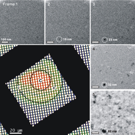
Fig. 1 depicts two types of images: five frames (1–5) obtained after exposure to fs pulses, and a lower magnification image obtained after a single laser pulse heated the material and induced regions of change (a, c, C, and i). These labels are placed on the image to indicate the different phases of amorphous, small-grain crystalline, large-grain crystalline, and interfacial. The artificial colors in the central image reflect contrast gradient, illustrating the spatial dependence in the transition from amorphous to crystalline phase. The inner and outer dotted circles are measured to be ≈35 μm and 77 μm, respectively, and they mirror the fluence gradient in the pulse and the specimen-dependent melting threshold. It is noted that the probe electron beam size for a typical single-pulse electron diffraction pattern is ≈70 μm in diameter, which is approximately the area indicated by the outer dotted circle. Frames 1–5 taken with fs irradiation show the onset of nucleation and grain growth, as evidenced in the increased grain size noted by dotted circles and by the change in contrast.
Fig. 1.
Image frames obtained by using fs and ns pulses. Frames 1–5 show the growth of crystallite size as the number of fs pulses increases, with the transition from amorphous (1) to polycrystalline (5) being evident in the images. The central colored image shows the response after a single laser-pulse heating. The zones are identified by circles to indicate the amorphous (a), the interfacial (i), and the two crystalline (c and C) phases. The C-zone diameter is 35 μm and the c-zone diameter is 77 μm (see text). The specimen in the microscope was thin films of amorphous silicon deposited on a grid by e-beam evaporation of a silicon wafer (also see Fig. 2).
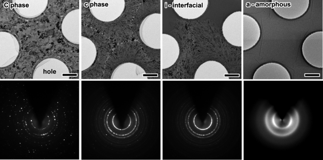
The structures in the regions a, c, C, and i are studied more in detail through real-space images and Fourier-space diffraction patterns. Fig. 2 is a display of images taken at higher magnification of the amorphous (a), interfacial (i), and the two crystalline (c and C) phases, together with the corresponding selected-area (6 μm) diffraction patterns of each zone. A broad halo ring characteristic of the amorphous phase is evident in a, and this halo ring can be easily observed by area selection everywhere on the specimen. After laser pulse heating, the diffuse amorphous patterns transform to sharp Debye–Scherrer rings or Bragg spots. The rings after crystallization are the averaged diffraction spots from a large number of diamond-type structures (nanocrystals) with random orientations. Nucleated nanocrystallites with the size of 10 nm are observed in phase c, whereas larger grains with the size of several hundred nanometers are observed in phase C, which is made in the area with the highest laser fluence. At the interface (i), there coexist the amorphous phase (upper region) and the crystalline phase (lower region). As noted in the diffraction frames, Bragg spots become most pronounced in phase C, in the static images displayed.
Fig. 2.
Images and electron diffraction patterns taken with the microscope at higher magnification (TEM) for the different phases of Fig. 1. (Scale bar: 1 μm.) All diffraction patterns were obtained by using a selected-area diffraction (SAD) aperture of 6 μm diameter of the specimen. The dark areas in the images are crystallites with orientation (of enhanced contrast) closely parallel to the incident electron beam. Holes are present in the polymeric substrate (and specimen), and their diameter is measured to be 2.4 μm. Note that the diversity in crystallinity in the diffraction images is reflected in the morphology.
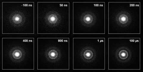
The time evolution of the single-pulse imaged frames taken during the structural change in crystallization is shown in Fig. 3. Each diffraction frame was obtained for a fresh specimen by translation in the specimen plane, keeping both the heating and electron pulses spatially and temporally under control. Observing the different phases (no aperture), the growth of well defined diffraction rings and the concomitant depletion of smooth broad rings are evident in the series of images recorded at different time delays. As such, these frames become the construct of a movie for the amorphous to the crystalline phase transition. At −100 ns, broad rings are observed, which are characteristic of the amorphous structure. With time, the sharp rings of the crystalline phase are observed directly in the frames (with no reference subtraction). The sharp rings are indexed to the (111), (022), and (113) planes of randomly oriented silicon crystallites.
Fig. 3.
Representative snapshots of the transformation. Shown are single-pulse diffraction images at different time delays. Each time frame has an exposure time of 15 ns, and all frames are for the same electron counts collected in each frame taken. Note the enhancement of scattering with time.
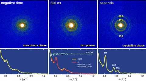
To quantify the spatiotemporal behavior, diffraction profiles were constructed from the radial average of respective diffraction images, all normalized to total electron count (Fig. 4). The images reflect the growth of crystallinity; i.e., the enhancement of diffraction peaks over the diffuse background. This is clear in the three frames shown as an example of the growth. The diffraction pattern at negative time and at seconds after heating (asymptote) displays this change of structure. A transient diffraction profile captured at, e.g., 600 ns after the arrival of the heating pulse is a linear combination of the two images at negative time (58%) and at the asymptotic (42%) time point (reminiscent of Vegard's law). The fit to the experimental results is satisfactory, suggesting the interconversion between the two phases. Accordingly, all obtained frames of transient change were handled similarly to provide the actual temporal change of the structure with time, the kinetic profile.
Fig. 4.
Diffraction representing three phases. (Upper) Diffraction before (Left), during (Center), and after (Right) the transformation, taken from the same sample area of irradiation. Three prominent diffraction rings are indexed in the image. (Lower) Radially averaged diffraction profiles of respective images shown above. To fit a transient-frame diffraction profile (Center), the negative-time (Left) and asymptotic profile (Right) are combined in proportion of their contributions. For the quality of a fit, the difference between the transient-frame profile and the fitted one is also depicted. The high signal-to-noise proved essential for the accuracy reported here.
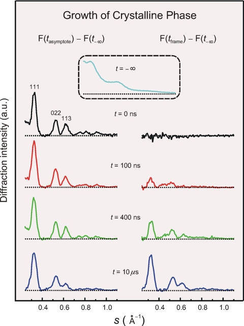
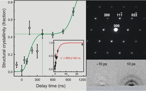
Shown in Fig. 5 are some representative frames of the growth. The patterns on the left are those taken at the asymptote time value minus a (smaller) scaled contribution of the averaged amorphous scattering at t = −∞; for all frames, the percentage of crystallinity at the asymptote is high, ≥67%. The patterns for F(tasymptote) − F(t−∞) do not change, whereas the transient frames on the right do change drastically with time. The contribution (fraction) of structural crystallinity for all frames taken is plotted against time in Fig. 6. The kinetic profile is rich—it shows an increase in the fraction but with structural features. If totally averaged, in a simple exponential rise fit, we obtained a characteristic time of 880 ± 140 ns for the final transformation on the time scale indicated.
Fig. 5.
Real-time evolution of the crystalline phase by using single-pulse imaging. Asymptotic (Left) and transient-frame (Right) diffraction profiles are obtained by eliminating the small contribution (box) of amorphous diffraction taken before heating (t = −∞). Note the similarity of the diffraction at the asymptote for all frames studied, while the diffraction for the phase change (Right) grows in amplitude with time. When deconvoluted from the instrumental response, the evolution of the width with time will provide the temporal changes in the size of crystallites.
Fig. 6.
Time-dependent growth of structural crystallinity. (Left) The fraction (circles) versus time gives the kinetic profile of the transformation. (Inset) Zoomed out kinetics over a longer time scale. The “averaged” exponential-rise fit of τ = 880 ns is depicted (solid line) in Inset. (Upper Right) Single-pulse diffraction pattern of single-crystal silicon taken with the incident electron beam parallel to the [011] zone axis. The single crystal on a grid was obtained (Mag*I*Cal Calibration Sample, SPI) and used as received. (Lower Right) Two time frames of diffraction difference at the time delays indicated. Referencing to the pattern at negative time, the frame at t = −10 ps displays no pattern, whereas the one at t = +10 ps shows the surface melting because of the ultrafast phase transition of the amorphous solid to the liquid phase (10). In the kinetic profile of crystallization, we note both the (averaged) exponential rise and the structured one (see text).
Finally, the single-pulse diffraction of a single crystal taken in our UEM apparatus is shown in Fig. 6 Right. This ability to observe crystallinity illustrates the appropriateness of lateral coherence of the single-pulse imaging, as mentioned above. We also include in the same figure two frames (10) for surface melting on the picosecond time scale, which indicate completeness of melting within the duration of the pulse used here at the supplied energy.
Crystallization Dynamics and Phase Transitions
The average energy density of the pulses used over the modified area of the specimen is estimated to be 100 mJ/cm2. At lower pulse energies than this “threshold,” the amorphous sample undergoes no crystallization, whereas at slightly higher energies, the silicon film is ruptured. Energy is deposited through the film thickness within the pulse; but at the low thermal conductivity of amorphous silicon (20), very minor energy flow out of the irradiated volume will occur over tens of microseconds (see below). Measured optical properties (20, 21) of amorphous silicon at 532 nm indicate ample absorption (α−1 ∼ 40 nm; n ∼ 4.8) in a 20-nm film for total melting, assuming all absorbed energy is converted to heat and confined within the film; a quantitative treatment of the heat balance requires full characterization of the role of the oxide layer, substrate, and calibration of specimen irradiation. The melting temperature for the crystalline phase is 1,687 K, whereas for the amorphous phase it is ≈200 K lower (20, 22, 23). The energy density threshold seen here for crystallization is similar to melting thresholds reported in many previous studies of ns irradiation of thick amorphous silicon films on thick silicon, silicon dioxide, or other substrates (20, 23–25), in which the heat spreads to depths of hundreds of nanometers, well beyond the skin depth for light absorption, within the duration of the pulse.
A fundamental characteristic of the environment in which crystallization takes place in the specimen is the temperature. A first-order approximation of the heat transport that takes place after the establishment, by absorption of the heating pulse, of an initial z-independent heat profile in the film is given by the 2D heat diffusion equation in a homogeneous medium. Assuming an initial Gaussian distribution of the temperature in amorphous silicon, the distribution in the absence of phase changes would evolve at later times according to
where r is the radial coordinate, t1/2 = r02/(4 ln 2D), r0 is the radius at half height of the initial distribution, and D = λ/(cVρ) is the heat diffusion constant for thermal conductivity λ. The quantity t1/2 represents the time for the axial temperature to drop to half its initial value, while temperatures of all other points in the region of interest drop more slowly.
For a thermal conductivity of relaxed amorphous silicon of 0.0065 W/(cm·K) (20), reasonable values of density ρ (26) and specific heat (20) and r0 ∼ 40 μm, one finds t1/2 = 1.57 ms; D ∼ 3.7 × 10⁻³ cm2/s. The same calculation for the polymeric Formvar substrate gives a longer relaxation time because of lower thermal conductivity. Radiative heat loss calculations at temperatures up to the melting temperature of silicon also indicate a very minor effect, showing that ≈1% of the calculated heat load would be lost in 10 μs. Thus, on the microsecond time scale there is a very limited heat dissipation in amorphous silicon. Once liquefaction or crystallization commences, heat transport within the modified volume will become faster because of an increase in λ, but the initially deposited heat will remain within the same volume to the extent that it is bordered by the original amorphous silicon, subject to transient losses to heat of fusion and ultimate additions of heat of crystallization.
This very restrictive heat dissipation environment makes the narrow window in pulse energy for nondestructive laser crystallization of our thin film understandable. Because we observe growth of large crystals in the region of maximum heating (zone C of Fig. 1), the super lateral growth regime of near complete melting is apparently reached in this area (27) while the film in zone c is heated to a temperature below that required for onset of crystallization. Because of the coexistence of melt and crystallites in zone C, the crystals grow to larger size. Given the fast change in crystallinity (see below), we must consider the mechanism of explosive crystallization (28) that is initiated in zone C and propagates out to create the larger area of fine-grained polycrystalline silicon, allowing for enhanced heat transport out of the hot center (23, 24). In this way, a flattening of the heat profile can result in all modified areas falling below the threshold for further crystallization within a few microseconds, as observed. A slight increase in deposited energy would push zone C into the regime of complete melting over significant areas and durations, compromising the physical integrity of the film.
As shown in many previous studies sensitive to surface melting, including an ultrafast electron crystallography study from this group (10), conversion of absorbed light energy to heat and the phase transition from the amorphous to liquid state occur on a time scale much shorter than the one reported here for crystallization, as revealed in Fig. 6 by diffraction difference images 10 ps before and after a fs heating pulse. Thus, the maximum extent of zone C melting must be reached by the end of the 17-ns heating pulse used here. At the same time, an outwardly propagating wave of explosive crystallization is launched, initially with a width of ≈250 nm at the speed of 15 m/s (see below).
The recorded structural crystallization transient of Fig. 6 reflects the fractional crystalline content of the entire area within the circumference of the ≈70-μm-diameter probing electron pulse. Increase in the signal comes both from the super lateral growth from liquid pockets (zone C) and explosive crystallization (zone c), with each having a distinct time evolution. At the interface, nucleated crystallites form the explosive front because of balance between latent heat of their crystallization and melting in neighboring amorphous structure. In zone C, the crystallization will occur at later times, but the released latent heat most probably will be nonexplosive given the time scale involved in cooling rates. Using a propagation speed for explosive crystallization of 10–20 m/s (23, 29), we may make a reasonable estimate of the appearance time of contributions from zone c. The crystal fraction distribution at t = +∞ is taken as uniform to a radius of 25 μm, then falling off to zero by 40 μm, consistent with the images of Fig. 2. Thus, the simple model of explosive crystallization starting at the edge of zone C (r = 17 μm) at t = 0 and traveling at 15 m/s across zone c to 35 μm yields a duration of 1.2 μs for contributions to the total signal from zone c alone, which is the time scale recorded in Fig. 6.
Taking a propagation time of ≈0.4 μs (Fig. 6) gives a distance in zone c of ≈6 μm and a 2D area accounting for ≈20% of the final signal, which is consistent with the explosive wave being effective to nearly half of the measured value at that time. The step observed in the kinetic profile appears to be from a delayed process, and we attribute it to the super lateral growth that is of slower nature. In comparing our step in structural crystallinity to some that have been reported in oscilloscope (bright field) detection (see ref. 12 and earlier references therein), although the time scale is similar, the signal-to-noise ratio does not permit us to comment on their origin. Clearly, future experiments will further explore the phase changes reported here, both spatially and temporally, given the fundamental questions pertinent to materials (30) and the relevance to the important silicon technology (31, 32).
Conclusion
The combined single-electron and single-pulse imaging in our ultrafast electron microscopy makes possible the study of reversible and irreversible structural dynamics. We exploit the single-pulse mode of operation to report here on the 4D visualization of nucleation and crystallization, as seen in the morphology (real space), and atomic-scale diffraction, during the transformation of amorphous to crystalline structure. The dynamical processes are resolved spatially and temporally. It is clear to us that this same approach is applicable to biological structures, including those that exhibit helicity effects in diffraction (33) and collapsed intermediate structures (34, 35). The concept discussed here of a “coherent” and “diffusive” search for native structures, through kinetic arrest of phase change, may turn out to be relevant in protein folding, as amorphous structures transform to their native ones.
Acknowledgments.
We thank Mr. Young Shik Shin for his help in the preparation of specimens and two referees for their helpful comments. This work was supported by the National Science Foundation, the Air Force Office of Scientific Research, and the Gordon and Betty Moore Foundation. Single-pulse biological imaging is supported in part by the National Institutes of Health.
Footnotes
The authors declare no conflict of interest.
References
- 1.Zewail AH. 4D ultrafast electron diffraction, crystallography, and microscopy. Annu Rev Phys Chem. 2006;57:65–103. doi: 10.1146/annurev.physchem.57.032905.104748. [DOI] [PubMed] [Google Scholar]
- 2.Shorokhov D, Zewail AH. 4D electron imaging: Principles and perspectives. Phys Chem Chem Phys. 2008;10:2879–2893. doi: 10.1039/b801626g. [DOI] [PubMed] [Google Scholar]
- 3.Thomas JM. In: Physical Biology—From Atoms to Medicine. Zewail AH, editor. London: Imperial College Press; 2008. p. 51. [Google Scholar]
- 4.Harris KDM, Thomas JM. Prospects for exploiting 4D ultrafast electron microscopy in solid-state organic and biological chemistry. Cryst Growth Des. 2005;5:2124–2130. [Google Scholar]
- 5.Park HS, Baskin JS, Kwon O-H, Zewail AH. Atomic-scale imaging in real and energy space developed in ultrafast electron microscopy. Nano Lett. 2007;7:2545–2551. doi: 10.1021/nl071369q. [DOI] [PubMed] [Google Scholar]
- 6.Lobastov VA, Weissenrieder J, Jau T, Zewail AH. Ultrafast electron microscopy (UEM): Four-dimensional imaging and diffraction of nanostructures during phase transitions. Nano Lett. 2007;7:2552–2558. doi: 10.1021/nl071341e. [DOI] [PubMed] [Google Scholar]
- 7.Gedik N, Yang D-S, Logvenov G, Bozovic I, Zewail AH. Nonequilibrium phase transitions in cuprates observed by ultrafast electron crystallography. Science. 2007;316:425–429. doi: 10.1126/science.1138834. [DOI] [PubMed] [Google Scholar]
- 8.Baum P, Yang D-S, Zewail AH. 4D visualization of transitional structures in phase transformations by electron diffraction. Science. 2007;318:788–792. doi: 10.1126/science.1147724. [DOI] [PubMed] [Google Scholar]
- 9.Carbone F, Baum P, Rudolf P, Zewail AH. Structural preablation dynamics of graphite observed by ultrafast electron crystallography. Phys Rev Lett. 2008;100 doi: 10.1103/PhysRevLett.100.035501. 035501. [DOI] [PubMed] [Google Scholar]
- 10.Ruan C-Y, Vigliotti F, Lobastov VA, Chen S, Zewail AH. Ultrafast electron crystallography: Transient structures of molecules, surfaces, and phase transitions. Proc Natl Acad Sci USA. 2004;101:1123–1128. doi: 10.1073/pnas.0307302101. [DOI] [PMC free article] [PubMed] [Google Scholar]
- 11.Zewail AH, Lobastov VA. Method and system for ultrafast photo-electron microscope. US patent 7,154,091. 2006;B2:20050401. [Google Scholar]
- 12.Bostanjoglo O, Marine W, Thomsen-Schmidt P. Laser-induced nucleation of crystals in amorphous Ge films. Appl Surf Sci. 1992;54:302–307. [Google Scholar]
- 13.Dömer H, Bostanjoglo O. High-speed transmission electron microscope. Rev Sci Instrum. 2003;74:4369–4372. [Google Scholar]
- 14.Kleinschmidt H, Ziegler A, Campbell GH, Colvin JD, Bostanjoglo O. Phase transformation analysis in titanium at nanosecond time resolution. J Appl Phys. 2005;98 054313. [Google Scholar]
- 15.LaGrange T, et al. Single-shot dynamic transmission electron microscopy. Appl Phys Lett. 2006;89 044105. [Google Scholar]
- 16.Siwick BJ, Dwyer JR, Jordan RE, Miller RJD. Ultrafast electron optics: Propagation dynamics of femtosecond electron packets. J Appl Phys. 2002;92:1643–1648. [Google Scholar]
- 17.Gahlmann A, Park ST, Zewail AH. Ultrashort electron pulses for diffraction, crystallography and microscopy: Theoretical and experimental resolutions. Phys Chem Chem Phys. 2008;10:2894–2909. doi: 10.1039/b802136h. [DOI] [PubMed] [Google Scholar]
- 18.Zewail AH. Visions of Discovery: New Light on Physics, Cosmology, and Consciousness. Cambridge, UK: Cambridge Univ Press; 2008. [Google Scholar]
- 19.Gai PL, editor. In-Situ Microscopy in Materials Research. Boston: Kluwer Academic; 1997. [Google Scholar]
- 20.Grimaldi MG, Baeri P, Malvezzi MA. Melting temperature of unrelaxed amorphous silicon. Phys Rev B. 1991;44:1546–1553. doi: 10.1103/physrevb.44.1546. [DOI] [PubMed] [Google Scholar]
- 21.Reitano R, et al. Transition from relaxed to derelaxed amorphous silicon: Optical characterization. J Appl Phys. 1993;74:2850–2855. [Google Scholar]
- 22.Donovan EP, Spaepen F, Poete JM, Jacobson DC. Homogeneous and interfacial heat release in amorphous silicon. Appl Phys Lett. 1989;55:1516–1518. [Google Scholar]
- 23.Thompson MO, et al. Melting temperature and explosive crystallization of amorphous silicon during pulsed laser irradiation. Phys Rev Lett. 1984;52:2360–2363. [Google Scholar]
- 24.Im JS, Kim HJ, Thompson MO. Phase transformation mechanisms involved in excimer laser crystallization of amorphous silicon films. Appl Phys Lett. 1993;63:1969–1971. [Google Scholar]
- 25.Im JS, Kim HJ. On the super lateral growth phenomenon observed in excimer laser-induced crystallization of thin Si films. Appl Phys Lett. 1994;64:2303–2305. [Google Scholar]
- 26.Custer JS, et al. Density of amorphous Si. Appl Phys Lett. 1994;64:437–439. [Google Scholar]
- 27.Kim HJ, Im JS. Multiple pulse irradiation effects in excimer laser-induced crystallization of amorphous Si films. Mat Res Soc Symp Proc. 1994;321:665–670. [Google Scholar]
- 28.Aleksandrov LN. Formation of semiconductor epitaxial films by pulse heating crystallization or regrowth. Phys Status Solidi A. 1983;76:179–190. [Google Scholar]
- 29.Geiler H-D, Glaser E, Götz G, Wagner M. Explosive crystallization in silicon. J Appl Phys. 1986;59:3091–3099. [Google Scholar]
- 30.Thompson MO, Aziz MJ, Stephenson GB, editors. Kinetics of Phase Transformation; Materials Research Society Symposium Proceedings; Pittsburgh: Materials Research Society; 1992. [Google Scholar]
- 31.Siffert P, Krimmel EF, editors. Silicon: Evolution and Future of a Technology. Berlin: Springer; 2004. [Google Scholar]
- 32.Hamann HF, O'Boyle M, Martin YC, Rooks M, Wickramasinghe HK. Ultra-high-density phase-change storage and memory. Nat Mater. 2006;5:383–387. doi: 10.1038/nmat1627. [DOI] [PubMed] [Google Scholar]
- 33.Lin MM, Shorokhov D, Zewail AH. Helix-to-coil transitions in proteins: Helicity resonance in ultrafast electron diffraction. Chem Phys Lett. 2006;420:1–7. [Google Scholar]
- 34.Ma H, Wan C, Wu A, Zewail AH. DNA folding and melting observed in real time redefine the energy landscape. Proc Natl Acad Sci USA. 2007;104:712–716. doi: 10.1073/pnas.0610028104. [DOI] [PMC free article] [PubMed] [Google Scholar]
- 35.Lin MM, Meinhold L, Shorokhov D, Zewail AH. Phys Chem Chem Phys. 2008 doi: 10.1039/b804675c. in press. [DOI] [PMC free article] [PubMed] [Google Scholar]


