Abstract
A simple fabrication technique was developed to produce high frequency (100 MHz) self-focused single element transducers with sputtered zinc oxide (ZnO) crystal films. This technique requires the sputtering of a ZnO film directly onto a curved backing substrate. Transducers were fabricated by sputtering an 18 μm thick ZnO layer on 2 mm diameter aluminum rods with ends shaped and polished to produce a 2 mm focus or f-number equal to one. The aluminum rod served a dual purpose as the backing layer and positive electrode for the resultant transducers. A 4 μm Parylene matching layer was deposited on the transducers after housing and interconnect. This matching layer was used to protect the substrate and condition the transfer of acoustic energy between the ZnO film and the load medium. The pulse-echo response for a representative transducer was centered at 101 MHz with a -6 dB bandwidth of 49%. The measured two way insertion loss was 44 dB. A tungsten wire phantom and an adult zebrafish eye were imaged to show the capability of these transducers.
I. INTRODUCTION
The development of medical ultrasonic transducers operating at frequencies greater than 100 MHz is quite a challenge. The quality of bulk piezoelectric materials and traditional machining techniques degrade as the desired device center frequency increases. Therefore, we chose to pursue piezoelectric thin film technology in order to simplify the transducer fabrication process and allow very high frequency transducers to be produced in a precisely controlled, repeatable manner.
ZnO and aluminum nitride (AlN) are two of the most common sputtered piezoelectric thin films used in ultrasonic transducers.1 Both materials exhibit a low relative dielectric constant (εS/ε0∼8) which is ideal for larger aperture single element transducers. However, ZnO has a larger electromechanical coupling coefficient (kt=0.28) than AlN (kt=0.17),2 which makes it the better choice for medical imaging transducer designs operating in thickness mode. Although neither material’s properties approach that of ferroelectric materials commonly used in single element transducers such as PbTiO3 and LiNbO3, ZnO and AlN are interesting alternatives for very high frequency designs because the sputtering process can be precisely controlled and is compatible with various substrates including silicon and metal.
Several groups have reported the development of ZnO-based ultrasonic delay-line transducers and arrays operating at 100-120 MHz.3-6 Polished flat sapphire or fused silica were used as a substrate for the ZnO film deposition. An electrode was first deposited on the substrate before sputtering the ZnO. An additional electrode was then directly deposited on the ZnO layer to complete the electrical connection. In order to improve image lateral resolution, a concave lens was formed by spherically3,4 or cylindrically5 polishing the other end of the substrate. The major drawback to this transducer design is that it generates internal sound wave reflections between the polished ends of the substrate. These reflections are detected by the ZnO and will degrade image quality if they cannot be suppressed or avoided. Acoustic matching layers can be deposited on the concave end to condition the transfer of acoustic energy between the lens and the load medium, which is typically water, and thus, reduce the amplitude of internal reflections. However, internal reflections caused by a delay-line-lens substrate can be avoided by shaping or self-focusing the piezoelectric material.
We have previously developed a technique to produce spherically shaped 200 MHz single element transducers by sputtered ZnO crystal films on a preformed Parylene diaphragm.7,8 The Parylene was etched away during the fabrication process for direct access to the ZnO layer and, thus, allowing the the use of an epoxy as the backing layer. Although this process produced highly focused, high frequency transducers, it required fourteen steps to complete. Therefore, the new fabrication process was developed to minimize the number of fabrication steps by sputtering ZnO directly on a highly polished spherically shaped metallic backing layer. We have demonstrated this simple technique for transducer manufacture before in a project the involved spin coating a thin layer of poly(vinylidine fluoride-trifluoroethylene) (P(VDF-TrFE)) on the curved metallic substrate to create 40 MHz transducers,9 however, it had yet to be tested with higher frequency sputtered thin films.
II. METHODS
A. Aluminum backing
Aluminum (Al) was selected as the backing substrate for several reasons: it is relatively soft and easy to machine, it is conductive, it has a melting point that is much higher than the operating temperature required for the ZnO sputtering process, and at 19 MRayls, its acoustic impedance is the lowest among the metals considered for this application.
The quality of our transducers greatly depended on the surface roughness of the shaped Al backing layer. The fabrication process started with machining 3.2 mm diameter Al into rods of approximately 15 mm in length. After machining, one of the two flat ends was polished to minimize surface imperfections. Highly polished chrome/steel ball bearings (4 mm diameter, grade 3, Bal-Tec, Los Angeles, CA) were then used with the aide of a hydraulic press (Carver, Wabash, IN) and custom made centering apparatus to press the spherical shape into the polished end. The rods were then machined on a lathe to their final dimensions of 2 mm in diameter and approximately 5 mm long. All surfaces other than the polished end were left rough to disperse backing echoes. A photograph of a fully processed Al backing substrate is shown in Fig. 1.
FIG. 1.
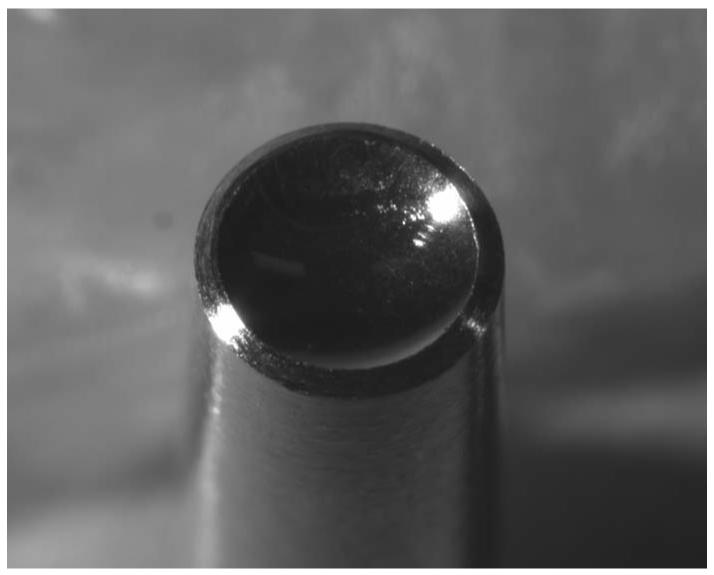
A photograph of the spherically polished end of an aluminum rod that was used as the backing substrate for the transducers.
B. ZnO deposition and Housing
A Materials Research Corporation (MRC) 822 Sputter-sphere sputtering machine was used to deposit the ZnO at approximately 0.5 μm/h with the following settings: O2 +Ar (50% +50%) gas at 10 mTorr, rf power of 230 W. Once cooled to room temperature, an unloaded epoxy was used to pot the ZnO+Al rod in brass cases attached to modified Sub-miniature Version A (SMA) female to female connectors. The SMA center conductor was attached to the Al rod with a small amount of silver epoxy. After housing, a thin layer of Cr/Au was sputtered over the exposed ZnO thin film and brass case to complete device interconnect and rf shielding. As shown in Fig. 2, the sputtered ZnO layer was 18 μm thick, corresponding to a theoretical unloaded resonance of approximately 175 MHz.2 Finally, a 4 μm Parylene C (Specialty Coating Systems, Indianapolis, IN) matching layer was vapor deposited over the electroplated ZnO layer as well as the housing.
FIG. 2.
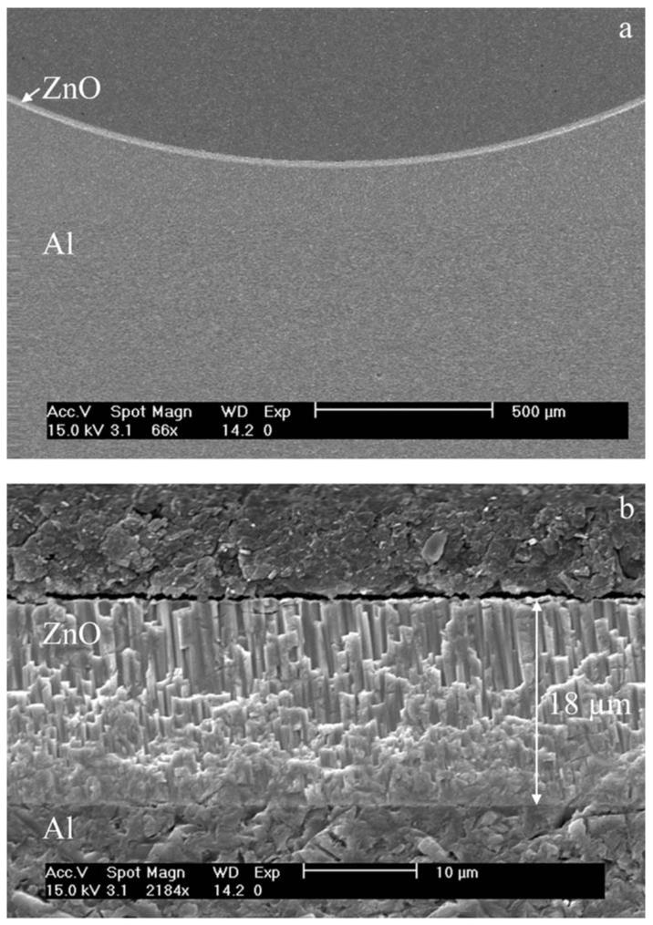
Scanning electron microscopy images of the ZnO film on the aluminum (Al) backing. The first image (a) shows the curvature of the Al backing and the second image (b) is a close-up view of the ZnO film.
C. Evaluation
The transducer pulse-echo response and insertion loss were measured in a room temperature de-ionized water bath by reflecting the transmitted signal off a polished x-cut quartz target placed at the focal point. A monocycle function generator (AVB2-TC-C, Avtech Electrosystems Ltd., Canada) was used as the transmitter by applying a 100 MHz, 90 Vp.p., single-cycle sine wave. The reflected waveforms were received by the transducers and digitized by a 500 MHz oscilloscope (LC534, Lecroy Corp., Chestnut Ridge, NY). The cables used to connect the transducers to the transmitter and the transmitter to the oscilloscope had a characteristic impedance of 50 Ω and were 20 and 28 cm, respectively. The system setup also included a diode expander and a limiter to protect the electronics as described in more detail by Lockwood et al.10 The insertion loss was calculated by comparing the frequency spectrum of the transmit and receive responses. Corrections were made for the attenuation in the water path and loss incurred by the imperfect reflection from the quartz target.11
An 8 μm tungsten wire (California Fine Wire Co., Grover Beach, Ca) was imaged using the setup described above in order to assess the axial and lateral resolution of the transducers. The remote amplifier portion of the Panametrics 5910 (Olympus NDT Inc., Waltham, Ma) set at 30.5 dB gain was used along with the LC534 as the receiver circuit. Piezoelectric actuators (Inchworm, Burleigh Inc., Fishers, NY) were used to linearly scan the wire across the transducer sound field with 0.5 μm steps. The amplified rf waveforms were recorded at each step by the LC534 and then used to form an image offline. The generated image was displayed using a logarithmic representation of pixel intensity with a 45 dB dynamic range.
The eyes of anesthetized adult zebrafish were also scanned with the transducers to show their capability to image tissue in vivo. For this test, the piezoelectric actuators were replaced by servo motors (SMAC LAR37, Carlsbad, CA) operating in swept mode. A low noise amplifier (Model 1466, Miteq Inc., Hauppauge, NY) with 35 dB gain, 12 bit ADC (CS12400, Gage Applied Technologies Inc., Lachine, QC, Canada), and PC with labview control was used for data acquisition. The lateral line spacing of the generated images was set at 5 μm for adequate sampling at the focus. Unfiltered zebrafish eye images contained gray or white artifacts at several image depths. These artifacts were not observed when the wire phantom image was generated. Therefore, it was concluded that the artifacts were caused by the electronic components and/or reverberations in the cabling used for the zebrafish imaging experiment. These electronically generated image artifacts were suppressed by subtracting the baseline image generated from the water bath only from the images of the zebrafish. High-pass and low-pass filters were also implemented to reduce random noise. All images were displayed with a 45 dB dynamic range.
III. RESULTS AND DISCUSSION
Three transducers were fabricated for this study. The results of the pulse-echo performance tests for these devices are displayed in Table I. The pulse-echo response for a representative transducer (transducer 2) was centered at 101 MHz with a -6 dB bandwidth of 49% (Fig. 3). The measured insertion loss for this transducer was 44 dB. Table I also includes results for a transducer (transducer 3) with and without the parylene matching layer. The addition of the parylene layer resulted in a slight reduction of the center frequency and bandwidth of this device, however, the measured insertion loss improved by 7 dB.
TABLE I.
Measured transducer performance whereby CF is the center frequency, BW is the -6 dB bandwidth, IL is the insertion loss, and PL is the -20 dB pulse length
| Transducer No. | CF (MHz) | BW (%) | IL (dB) | PL (ns) |
|---|---|---|---|---|
| 1 | 107 | 43 | 45 | 37 |
| 2 | 101 | 49 | 44 | 32 |
| 3 | 105 | 51 | 47 | 31 |
| 3(no Parylene) | 109 | 52 | 54 | 36 |
FIG. 3.
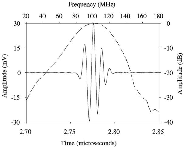
Measured pulse-echo waveform (solid line) and spectrum (dashed line) for transducer 2.
Figure 4. shows the wire target image and the axial and lateral line spread functions with the wire placed at the focus of transducer 1. The measured -6 dB resolutions estimated from the line spread functions were 14.4 μm in the axial direction and 16.7 μm in the lateral direction. Figure 5 shows a zebrafish eye image, also generated by transducer 1, showing the cornea and iris. In Fig. 6, the inner and outer surfaces of the cornea are more clearly visible. From this image, it was determined that the cornea was approximately 30 μm thick.
FIG. 4.
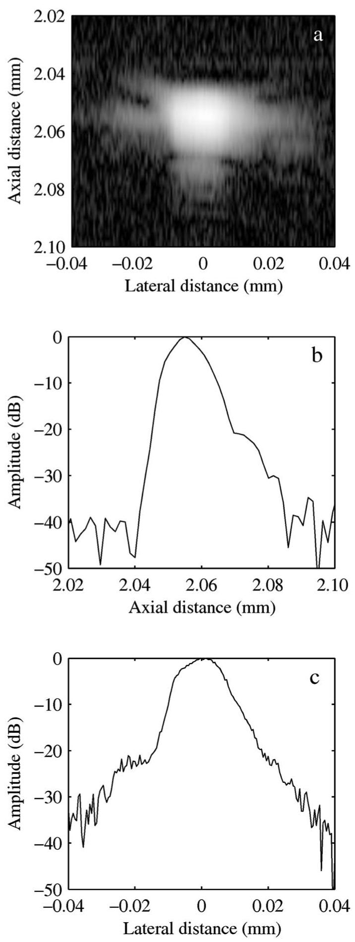
Wire target image acquired with transducer 1 (a), as well as the two-way axial (b) and lateral (c) line spread functions.
FIG. 5.
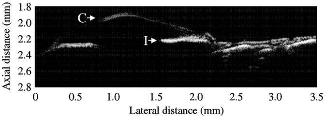
Zebrafish eye image aquired using transducer 1. The cornea (C) and iris (I) are visible in this image.
FIG. 6.
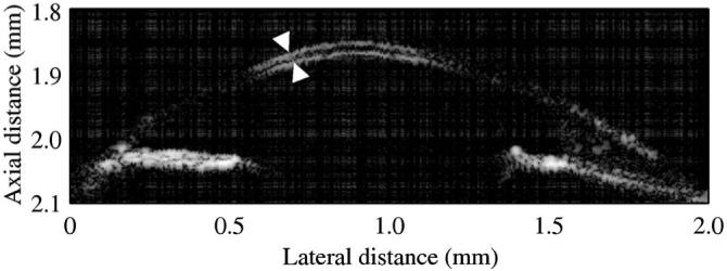
Zebrafish eye image aquired using the transducer 1 that clearly shows the inner and outer surfaces of the cornea (arrows).
A simple transducer fabrication technique utilizing sputtered ZnO thin films was demonstrated. We believe that this technique has the potential to help (>100 MHz) ultrasonic biomicroscopes become more readily available in the future. However, in order for this potential to be realized, the insertion loss of these transducers must be reduced to improve image quality. A significant amount of energy is lost in the aluminum backing. Typical insertion loss levels for high frequency single element ultrasonic transducers range from 10-25 dB when LiNbO3 is used as the active material,11 and up to 40 dB when P(VDF-TrFE) is used.9 Future efforts will be focused on incorporating an additional higher impedance sputtered or spin coated acoustic matching layer to further reduce losses during transmission and reception.
ACKNOWLEDGMENTS
The authors would like to thank Hyung-Ham Kim and Chang-Hong Hu for their help with the wire phantom imaging experiment, as well as the National Institutes of Health for providing the funding for this project through Grant No. P41-EB2182.
References
- 1.Trolier-McKinstry S, Muralt P. J. Electroceram. 2004;12:7. [Google Scholar]
- 2.Kino G. Acoustic Waves: Devices, Imaging, Analog Signal Processing. Prentice Hall, Englewood Cliffs, NJ: 1987. [Google Scholar]
- 3.Kushida K, Takeuchi H, Kanda H, Yamaguchi S. Jpn. J. Appl. Phys. 1989;28(Part 1):260. [Google Scholar]
- 4.Yokosawa K, Shinomura R, Sano S, Ito Y, Ishikawa S, Sato Y. Ultrason. Imaging. 1996;18:231. doi: 10.1177/016173469601800401. [DOI] [PubMed] [Google Scholar]
- 5.Ito Y, Kashida K, Sugawara K, Takeuchi H. IEEE Trans. Ultrason. Ferroelectr. Freq. Control. 1995;42:316. [Google Scholar]
- 6.Martin PM, Good MS, Johnston JW, Posakony GJ, Bond LJ, Crawford SL. Thin Solid Films. 2000;379:253. [Google Scholar]
- 7.Feng GH, Sharp CC, Zhou QF, Pang W, Kim ES, Shung KK. J. Micromech. Microeng. 2005;15:586. [Google Scholar]
- 8.Zhou QF, Sharp CC, Cannata JM, Feng GH, Kim ES, Shung KK. Appl. Phys. Lett. 2007;90:113502. [Google Scholar]
- 9.Robert M, Molingou G, Snook K, Cannata J, Shung KK. J. Appl. Phys. 2004;96:252. [Google Scholar]
- 10.Lockwood GR, Hunt JW, Foster FS. IEEE Trans. Ultrason. Ferroelectr. Freq. Control. 1991;38:48. doi: 10.1109/58.67834. [DOI] [PubMed] [Google Scholar]
- 11.Cannata JM, Ritter TA, Chen W-H, Silverman RH, Shung KK. IEEE Trans. Ultrason. Ferroelectr. Freq. Control. 2003;50:1548. doi: 10.1109/tuffc.2003.1251138. [DOI] [PubMed] [Google Scholar]


