Abstract
The optical properties of hollow nanoparticles (Au–Ag nanoboxes and nanocages) were investigated by recording Rayleigh scattering spectra of single particles, whose morphology and composition had been analyzed by scanning electron microscopy (SEM). This was achieved by depositing the particles on optically transparent substrates with registration marks, which are compatible with SEM imaging. Fitting the experimental spectra to a Lorentzian function yields the frequencies and homogeneous line widths of the plasmon resonance for the particles. The resonances are extremely broad, with dephasing times of 2–5 fs. Analysis of the line width data using the dimensions determined by SEM shows that the broadening is due to a combination of electron–surface scattering and radiation damping. The sensitivity of the plasmon resonance to the dielectric constant of the environment was also investigated by adding a drop of water to the substrate. The nanoboxes show similar dielectric sensitivities compared to other metal nanoparticle systems. A significant increase in the line width was also observed for the nanoboxes in water compared with air. This was attributed to increased radiation damping in the environment with a higher dielectric constant. Both the red shift and the increase in line width are reversible.
1. Introduction
The optical properties of noble metal nanostructures have attracted considerable interest in both fundamental and applied sciences.1-5 The distinct colors of these systems arise from the localized surface plasmon resonance (LSPR), which is a collective oscillation of the conduction electrons in the metal. The position of this resonance varies over a broad spectral range depending on the metal.1,2 In particular, the optical properties of gold and silver nanoparticles and their alloys have been extensively studied, because of their strong resonances in the visible region.2,3,6 Additional control of the position of the LSPR peak can be achieved by preparing particles with different sizes and shapes.7-10 For example, triangular silver plates have red-shifted resonances compared with spheres,8 and spherical gold nanoshells supported on a dielectric silica core have resonances that are tunable from the visible to the near-infrared region.10
The plasmon resonance can also be modified by changing the particle’s environment, which has led to applications in molecular sensing.11 In single particle sensing measurements, it is important to have resonances with high quality factors Q = Eres/Γhom, where Γhom is the homogeneous line width and Eres is the resonance energy. The homogeneous line width is controlled by lifetime broadening due to different plasmon decay channels and is given by Γhom = 2ℏ/T2, where T2 is the dephasing time of the LSPR.12 The study of the dephasing process can be conducted in either the time or the frequency domains.13 However, time-resolved measurements of LSPR dephasing are difficult to perform because of the ultrafast timescales;14 thus, the dynamics of these systems are much better studied in the frequency domain.
Spectroscopic studies of plasmon dephasing in metal nanoparticles were first reported almost 50 years ago for ensemble samples.15 Recent progress and interest in optical microscopy has enabled the study of single metal nanoparticles.16,17 These experiments provide much more accurate information compared with conventional ensemble measurements, because of the reduction of inhomogeneous broadening effects from different sizes and shapes in the sample. In these studies, the nanoparticles are deposited on a substrate at low concentration to avoid particle aggregation, and dark-field or total internal reflection illumination is employed to record the scattering spectra of the particles.16,17 However, the sensitivity of the LSPR to size and shape means that it is important to have structural information about the particle being interrogated for quantitative analysis of the data.18
In a recent paper, we examined the plasmon resonances of Au–Ag nanoboxes by single particle Rayleigh scattering spectroscopy.19 These particles had very broad spectra, which was attributed to a combination of electron–surface scattering20,21 and radiation damping effects.12,22 We did not correlate the measured Rayleigh scattering spectra to structural analysis of the particles in these experiments. Instead, we measured the average size of the nanoparticles via transmission electron microscopy (TEM) and correlated this to the average line width from the optical experiments.19 This procedure did not yield very precise information about the electron–surface scattering and radiation damping processes in these materials. Furthermore, even though the solution was dilute enough to achieve the single nanoparticle level, we cannot rule out that we were actually detecting aggregates of particles. This is a significant concern, given that the measured spectra were unusually broad.19
In this paper, we present scattering spectra from single nanoboxes and nanocages whose size, shape, composition, and orientation on the substrate have been measured by scanning electron microscopy (SEM). The SEM analysis ensures that only single particles, not dimers or trimers, are studied. The particles in these experiments had edge lengths between 80 and 160 nm, with plasmon resonances in the range of 1.5–1.8 eV. This is well away from the interband transitions of Ag and Au,1,4 which means that the bulk contributions to the line width are minimized. Analysis shows that both electron–surface scattering and radiation damping are important for these particles. We also present studies of the sensitivity of the plasmon resonance for the Au–Ag nanoboxes to the dielectric constant of the environment.
2. Experimental Section
Preparation and Characterization of Samples
The synthesis of Au–Ag nanoboxes and nanocages is described in detail in ref 23. In order to perform the optical and electron microscopy analysis, the particles were deposited on indium tin oxide (ITO) coated glass substrates (SPI Supplies). These substrates are conductive enough for SEM measurements and are optically transparent in the visible region. A designed pattern on a photomask was transferred into metal marks by thermal evaporation of a 15 nm thick Au layer onto the ITO substrate. This registration substrate was immediately sonicated in water to remove dust from the surface and then rinsed with deionized water and ethanol. A drop of diluted nanoparticle solution (10 × from the as-synthesized solution) was placed on the area nearby the registration marks on the surface of the ITO substrate. This drop was immediately removed using a micropipet. The sample substrate was allowed to dry at room temperature and carefully stored in a nitrogen environment to inhibit oxidation of the particles. Secondary electron SEM (SE-SEM) images and back-scattering SEM images were obtained using a field-emission microscope (Sirion XL, FEI, Hillsboro, OR) operated at 5 kV. The composition of the nanoparticles was analyzed using an energy dispersive X-ray microanalysis (EDAX) system incorporated with the Sirion electron microscope. The acceleration voltage was set at 5 kV. The AuM and AgL lines were used to measure the contents of Au and Ag in the particles, respectively. TEM images of the particles presented in Supporting Information were recorded with a Philips 420 transmission electron microscope operated at 120 kV.
Optical Studies: Single Nanoparticle Spectroscopy
An Olympus IX-71 inverted optical microscope was used for dark-field microscopy. The illumination light comes from the output of a 100 W halogen lamp with a dark-field oil-immersion condenser (Olympus U–DCW). The condenser forms a hollow cone of light focused at the plane of the sample. Only light that is scattered out of this cone reaches the objective. The Rayleigh scattering from a single nanoparticle was collected with a 60 × objective and directed to the entrance slit of an imaging monochromator (Acton Research MicroSpec 2150i) equipped with a Roper Scientific 100 × 1340 B liquid N2 cooled CCD camera. The scattered light was first imaged on the CCD using a mirror to ensure the target particle was chosen. The mirror was then replaced by a grating (150 grooves/mm, blaze wavelength 800 nm) to disperse the collected light. Normalized Rayleigh scattering spectra from individual particles were obtained by subtracting and dividing by a background, taken from a nearby area of the CCD detector (identical pixel width but without particles). The acquisition times for the spectra were between 10 and 20 s. Most of the experiments were conducted in an air environment. For experiments in water, a drop of MilliQ water was applied to the sample, and a cover slip was then placed on top of the water. The spectra obtained were fit to a Lorentzian function using the “solver” routine in Microsoft Exel.
3. Results and Discussion
3.1. Rayleigh Scattering Spectra of Nanoparticles in Air
In general, one cannot determine whether a diffraction-limited spot in a microscope image represents a single particle or an aggregate of particles. The registration substrate provides a way of finding a specific nanoparticle in both the SEM and the dark-field images, ensuring that only isolated particles are analyzed in the Rayleigh scattering measurements. Figure 1 shows the side and top views of the pattern on a representative registration substrate. The plasmon resonances of the nanoboxes and nanocages used in these experiments occur in the visible to near-infrared region,24 which means that the particles appear as red/orange dots under the dark-field microscope. Figure 2A shows a true color image of several nanocage particles under dark-field illumination, which display a reddish or orange-red color. The corresponding SEM image of this area of the substrate is shown in Figure 2B. The close correspondence between the patterns in the optical and SEM images means we can unambiguously correlate these two measurements.
Figure 1.
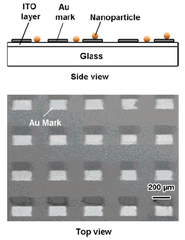
Top panel shows the side view of the registration substrate used in the experiment. The lower panel shows a top-view SEM image of the substrate. The squares are the gold marks used to locate specific nanoparticles on the substrate.
Figure 2.
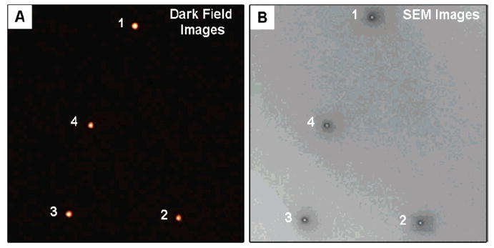
(A) True color image of a particle pattern recorded by dark-field microscopy. (B) SEM image of the same particle pattern.
The secondary electron/back-scattering SEM imaging and EDAX microanalysis allow us to determine the edge length, morphology (presence or absence of facets and holes), and elemental composition of specific nanoparticles. For nanoboxes, it is also possible to measure the wall thickness from these measurements. Figure 3 shows an example of the correlated SEM/optical analysis. The secondary electron SEM image in Figure 3A shows that this particle is a cubic nanobox, with an edge length of 99 nm. Figure 3B is a back-scattering SEM image, which allows us to “see through” the structure and determine a wall thickness of 12.6 nm. Figure 3C shows the results of EDAX elemental analysis of the nanobox, which yield an atomic ratio of Au/Ag = 1:2. Elemental analysis is important for these measurements, because the dielectric constant of the particle depends on the Au/Ag ratio.25 For metal particles, the resonance energy is determined by the real component of the dielectric constant, and the line width is primarily controlled by the imaginary component.1,26 The optical scattering spectrum of the nanobox is shown in Figure 3D. A fit to the measured spectrum using a Lorentzian function is also included in the figure. The resonance energy and homogeneous line width obtained are Eres = 1.72 eV and Γhom = 338 meV. The deviation between the measured spectrum and the Lorentzian fit at low energies is due to a cutoff in our instrument response function.
Figure 3.
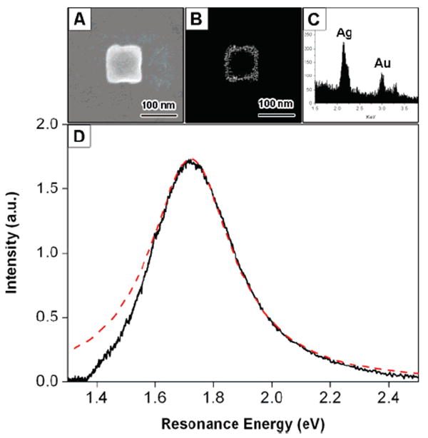
(A) Secondary electron SEM image of a Au–Ag nanobox. (B) Back scattering SEM image of the nanobox. The wall thickness can be determined from the image. (C) EDAX data of the nanobox, giving a Au/Ag ratio of 1:2. (D) Optical scattering spectrum recorded using dark-field microscopy. The dashed line shows a Lorentzian fit to the spectra.
Figure 4 shows high-resolution SEM images and Rayleigh scattering spectra for the Au/Ag nanocages in Figure 2. In comparison to the nanoboxes, the nanocages have truncated corners, which gives rise to {111} facets. The overall shapes of the nanocages range from cuboctahedral to a truncated octahedron, depending on the relative size of the {111} facets. Holes with dimensions on the order of 10 nm can clearly be seen on the {111} facets of the nanocages.24 These holes presumably allow solvent inside the particle to exchange with the environment. Note that the wall thickness cannot be accurately measured from back-scattering SEM images for the nanocages, because of the presence of both {111} and {100} surfaces on the particle. TEM analysis of the nanocage samples used in these experiments shows that the wall thickness is proportional to the edge length: w = 0.11 × L − 2.4 (see Supporting Information for details). Note that we occasionally observed small “shoulders” on the blue side of the spectra, for example, particle #2 in Figure 4B. These features are tentatively assigned to the quadrupole resonance of the particle.4 It is not clear why some nanoparticles show this resonance and others do not. This may be due to the interaction of the particles with the substrate27 or because of some internal structures of the particles.
Figure 4.
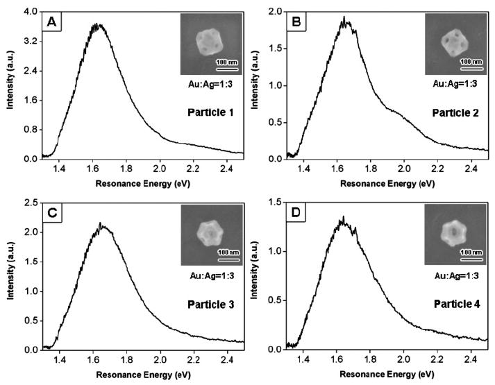
SEM images (shown as insets), elemental composition, and spectra for particles No. 1–4 shown in Figure 2. The orientations of particles 1 and 2 ({100} facets in contact with the substrate) are different than those for particles 3 and 4 ({111} facets in contact with the substrate).
There are several points to note from Figure 4. First, the faceted structure of the nanocages means that they have two possible orientations on the substrate, and this can be clearly seen in Figure 4. Particles #1 and #2 have their {100} surfaces contacting the substrate (we label this orientation as type I nanocages); while particles #3 and #4 contact the substrate through their {111} surfaces (labeled as type II nanocages). This difference in orientation is illustrated in Figure 5. Whether a nanocage is type I or type II depends on the relative size of the {111} facets compared with the {100} facets: nanocages that have {100} facets dominant are type I, and nanocages with {111} facets dominant are type II. Also note that the spectra, especially at lower energies, are distorted because of the instrument cutoff in our detection system. Therefore, the homogeneous line widths Γhom were obtained by only fitting the higher energy side of the spectra.
Figure 5.
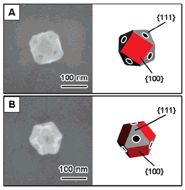
Different orientations of the nanocages on the substrate. (A) A nanocage with a {100} surface contacting the substrate (type I). (B) A nanocage with a {111} surface contacting the substrate (type II).
Figure 6 shows an SEM image and Rayleigh scattering spectrum from a representative nanoparticle dimer (in this case two type I nanocages). The peak in the LSPR of the dimer occurs in a similar spectral position to the monomers. Thus, for these particles, it is not possible to distinguish between dimers and monomers solely from the resonance frequency. The line width for the dimer is ~550 meV, which is significantly broader than the typical line widths measured for the monomers.
Figure 6.
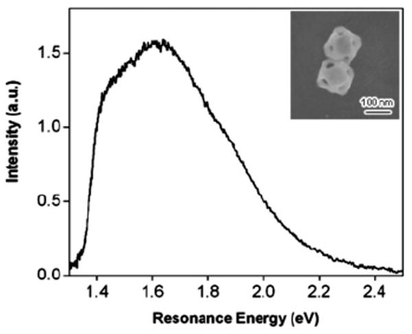
Rayleigh scattering spectra and SEM image of a nanoparticle dimer. The two particles are orientated with their {100} surfaces in contact with the substrate (type I nanocages).
Figure 7 shows a plot of the measured resonance energies and line widths versus the edge length for all of the nanoboxes and nanocages examined (only single nanoparticle data are included, no dimers or trimers). The resonance energies occur between 1.50 and 1.80 eV, which is consistent with the plasmon peaks observed in the ensemble measurements. The nanocages have slightly red-shifted resonance energies (on average) compared with the nanoboxes. This is most likely because the nanocages have slightly larger edge length to wall thickness ratios.24 The average edge length to wall thickness ratio is L/w = 8 for the nanoboxes, compared with L/w = 11 for the nanocages (see Supporting Information). On the other hand, the line widths are very similar for the nanocages and nanoboxes. The line widths vary from 270 to 520 meV, which corresponds to dephasing times on the order of 2–5 fs. This is comparable to the results reported by Sonnischen et al. for solid gold nanoparticles with >40 nm diameter12,22 and those for the gold nanoshells studied by Halas and co-workers.28 The average line widths for the different samples are Γ̄ = 360 ± 52 meV for the nanoboxes, Γ̄= 424 ± 67 meV for the type I nanocages, and Γ̄ = 376 ± 65 meV for the type II nanocages (errors equal the standard deviation). The average line width for the nanoboxes is consistent with the results from our previous study.19 There does not appear to be a strong correlation between the line widths and the edge lengths (see Figure 7).
Figure 7.
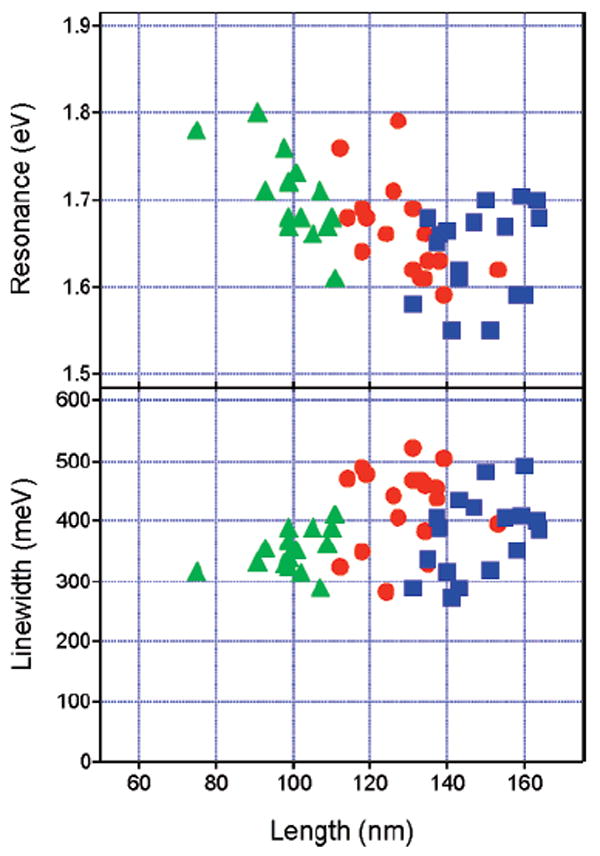
Resonance energy (Eres, top) and line width (Γhom, bottom) versus edge length for the nanoboxes and nanocages examined in the single nanoparticle experiments. Green triangles = nanoboxes; red circles = type I nanocages; blue squares = type II nanocages.
3.2. Data Analysis
The particles in this study have dimensions (wall thicknesses and edge lengths) where both electron–surface scattering and radiation damping effects are expected to be important.20,21 To understand how these processes affect the spectra, the line width is expressed as a sum of contributions from bulk dephasing, electron–surface scattering, and radiation damping:1,19
| (1) |
where ∈1 and ∈2 are the real and imaginary components of the bulk dielectric function, υF is the Fermi velocity, Leff is the effective path length of the conduction electrons, V is the volume, and A and k are constants that characterize the electron–surface scattering and radiation damping processes, respectively. In our analysis, we use Leff = 2w, where w is the wall thickness.19 This is appropriate for a flat plate and is consistent with the expression Leff = 4V/S recently derived for convex particles.29,30 Previous studies have shown that the nanoboxes generated from our synthesis are alloys, rather than core–shell structures.7 Thus, for Γbulk, ∈1 and ∈2 were calculated by averaging the dielectric constant of pure gold and silver,31 according to the atomic ratio determined from the EDAX analysis.32 This yields a value of Γbulk = 75 meV.19
We first discuss the line width data for the nanoboxes. In our previous study, a surface scattering coefficient of A = 2 ± 1 and a radiation damping constant of k = (9 ± 5) × 10−7 fs−1 nm−3 were obtained by analyzing the average line width data from nanobox samples with different dimensions.19 Here, we use the correlated SEM/optical measurements to generate values for the volume and effective path length for each particle. The data set consisting of the line widths, volumes, and Leff values are then fitted using eq 1. The electron–surface and radiation damping parameters obtained from this analysis are A = 3.6 ± 0.4 and k = (1.9 ± 0.2) × 10−7 fs−1 nm−3. The measured value of k is close to the value of k = 3.6 × 10⁻⁷ fs−1 nm−3 determined by discrete dipole approximation (DDA) calculations of nanoboxes.19 However, the value of A is significantly larger than the surface scattering parameters determined for other systems.20,21,30 For example, recent single particle experiments on gold spheres and gold nanorods gave a surface scattering parameter of A = 0.30 ± 0.03.20,21 The larger value of A for the nanoboxes may indicate that the expression Leff = 2w is not appropriate for these particles. The surface scattering parameter derived for the nanoboxes can be refined if a more rigorous expression for Leff becomes available. To this end, the dimensions, line widths, and resonance energies of all of the particles examined in this study are given in Supporting Information. It is also possible that the nanoboxes have a complicated internal structure that is not visible by SEM but affects the electron–surface scattering process.
This analysis was not performed for the nanocages, because we do not have independent measurements of the wall thickness for the individual particles studied in the optical experiments. Instead, for the nanocages, we use the average dimensions determined from the SEM and TEM analysis and the values of A and k obtained from the nanoboxes to calculate the electron–surface and radiation damping contributions. The values obtained are meV and meV for the type I particles and meV and meV for the type II particles. In this analysis, the average volume was calculate by , where the factor of 5/6 in the first term arises from treating the nanocages as cuboctahedra,33 and the second term accounts for the holes on the {111} facets (d is the diameter of the holes measured by SEM). This gives total calculated line widths of Γcalc = 411 meV for the type I nanocages, and Γcalc = 495 meV for the type II nanocages. The calculated line width is in excellent agreement with the average value of Γ̄ = 424 ± 67 meV measured for the type I nanocages but is larger than the value of Γ̄ = 376 ± 65 meV determined for the type II nanocages. The deviation for the type II nanocages probably arises because these particles have a higher degree of truncation compared with the type I nanocages. Thus, treating the type II nanocages as cuboctahedra overestimates their volume and, therefore, overestimates the magnitude of the radiation damping effect.
3.3. Particles in Water
The optical properties of metal nanoparticles also depend strongly on the local environment.1-4 We have investigated the sensitivity of the LSPR to the dielectric environment by measuring spectra of nanoboxes and nanocages in air (n = 1.0) and water (n = 1.33). Figure 8 shows typical spectra for both types of particles. As expected, the spectra are red shifted in water. For the nanoboxes, the magnitude of the red shift is consistent between different particles, ranging from 90 to 160 meV. For the nanocages (Figure 8B,C), the red shifts show much larger variations. The nanocage spectra were also often distorted, either upon adding water or after drying. Finally, in several cases (such as in Figure 8C), the red shift moves the spectra outside the range of our instrument response function, leading to highly distorted spectra. Thus, in the discussion below, we concentrate on the solvent dependence of the nanobox spectra.
Figure 8.
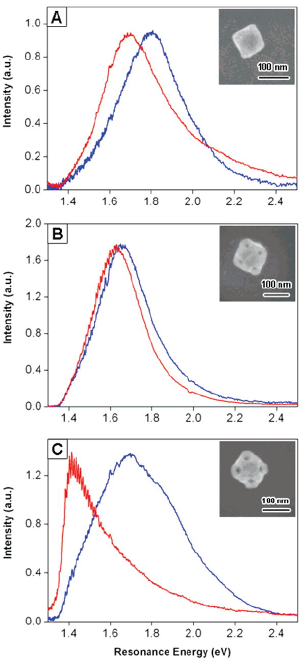
Local environment dependence of the LSPR for (A) a nanobox particle, and (B) and (C) two nanocage particles. Blue spectra correspond to an air environment, while the red ones were taken in a water environment. The insets are the SEM images of the particles.
The dielectric sensitivity of the LSPR can be characterized by the shift in the plasmon peak position per unit of refractive index change; in energy units this is: m = ΔEres/Δn (meV/RIU).34 The average red shift for the nanoboxes is 120 ± 20 meV, which gives a dielectric sensitivity of m = 360 ± 60 meV/RIU. This is consistent with recent studies of the dielectric sensitivity of the dipole resonance in single silver triangles.34 An important factor in evaluating the potential use of metal nanoparticles for sensing applications is the figure-of-merit (FOM) introduced by van Duyne and co-workers, which is the dielectric sensitivity divided by the line width: FOM = m (meV RIU − 1)/Γ (meV).34 Materials with high FOMs allow accurate measurement of the change in dielectric constant of the environment. The FOMs for the nanoboxes fall in the range of 0.8 to 1.4, with an average value of 1.1 ± 0.2. These values are two to three times worse than the FOMs for the dipole resonances of silver triangles, and this is almost entirely due to the broader line widths of the LSPR for the nanoboxes compared with the triangles.34
Figure 9A shows a plot of the line widths versus resonance energy for the nanoboxes in air and water. This plot clearly demonstrates the red shift in the resonance due to the increase in the dielectric constant of the environment. Furthermore, the data shows that the line width of the LSPR increases when the particles are immersed in water. The average line width for the particles changes from 360 ± 52 meV for air to 428 ± 48 meV for water, an increase of approximately 20%. The inset of Figure 9A shows a plot of the change in line width (ΔΓ) versus the magnitude of the red shift of the LSPR for all of the nanoboxes examined.
Figure 9.
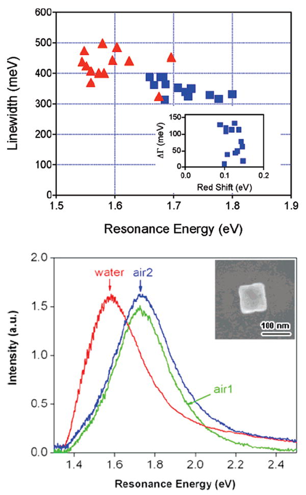
(A) Top: Line width versus resonance energy for nanoboxes in air (blue squares) and in water (red triangles). The inset shows the change in line width (ΔΓ) plotted against the magnitude of the red shift of the LSPR (ΔE). (B) Bottom: Rayleigh scattering spectra of a nanobox in air (air 1), in a water environment, and in air again (air 2) after drying the substrate. The resonance energies changed from 1.72 → 1.58 → 1.73 eV, and the line widths from 324 → 401 → 359 meV in the order of air 1 → water → air 2. The inset shows the SEM images of this nanobox.
Figure 9B shows an experiment where we recorded spectra for a particle in air, then in water, and finally in air again after allowing the sample to dry. The spectrum essentially returns to its original position and shape. There is a slight blue shift and a small change in the line width, which may indicate either some reconstruction of the structure during the experiment27,34 or incomplete escape of solvent inside the particle during drying. This reversibility demonstrates that the increase in line width observed upon adding water is not due to major structural changes in the particles.
It seems unlikely to us that the changes in the line width arise from changes in the electron–surface interaction: water is not considered to give large chemical interface damping effects.1,4,35 It is also unlikely that the increase in line width comes from changes in the bulk damping contribution brought about by the red shift in the LSPR frequency. Calculations of Γbulk using the dielectric constants of silver and gold show very little frequency dependence in the near-IR/visible spectral region. Thus, the most likely explanation for the increase in the line width in water is radiation damping.
Theoretical results for radiation damping in spherical particles predict that Γrad should be proportional to the refractive index of the medium.36 For particles supported on a substrate, both the refractive index of the support and the solvent need to be taken into account. This is typically done by writing the effective refractive index as nmed ∝ (1 − α) × ni + α × nITO,37 where nITO is the refractive index of the substrate, ni represents the solvent (either air or water), and α gives the relative contributions of the two. For nITO = 2,38 α must be less than or equal to 0.1 to explain the 20% increase in the overall line width (this calculation assumes that α is the same for the air and water environments). This implies that the effective refractive index felt by the particles is dominated by the solvent.
An increase in line width with increasing dielectric constant of the environment has not been reported in previous single particle solvent dependence studies,34 presumably because the particles were too small to display significant radiation damping effects. This explanation for the increase in line width can be easily tested through DDA calculations of the optical response of metal nanoboxes.
4. Summary and Conclusions
Rayleigh scattering spectra of individual hollow cubic structured nanoparticles were measured by dark-field microscopy. A registration substrate was used to correlate the spectral measurements to SEM images of the particles. This enabled us to precisely determine how the homogeneous line width depends on the dimensions and morphology of the particles. Two types of particles were studied: Au/Ag nanoboxes (hollow cubes) and nanocages (nanoboxes where the corners have been truncated to give {111} facets, and holes have developed on these facets). The nanocages sit with either their {100} facets in contact with the substrate (type I nanocages) or with their {111} facets in contact with the substrate (type II nanocages). Which orientation occurs depends on the relative size of the {111} and {100} surfaces. The type II nanocages are significantly larger than the type I nanocages, but the measured line widths do not show any trend with size.
The experimental line width data for the nanoboxes was analyzed using , where the first term corresponds to the bulk contribution to plasmon damping, and the second and third terms account for electron–surface scattering and radiation damping, respectively. In our analysis, the volume V and effective path length Leff were directly determined from the SEM images of the particles. The values of the surface scattering and radiation damping parameters determined were A = 3.6 ± 0.4 and k = (1.9 ± 0.2) × 10−7 fs−1 nm−3. These results show that both radiation damping and electron–surface scattering make significant, and almost equal, contributions to the line width.
Calculated values of the line width for the nanocages using the average dimensions obtained from TEM and SEM analysis, and the values of A and k determined for the nanoboxes, are in good agreement with the experimental line widths for the type I nanocages but are significantly larger than the experimental values for the type II nanocages. We believe that our calculations overestimate the volume for the type II nanocages (both the type I and the type II particles are treated as hollow cuboctahedra) and, therefore, overestimate the radiation damping effect for these particles.
The sensitivity of the plasmon resonance to the local environment was also studied for the nanoboxes by immersing them in water. The spectra show a red shift, with a dielectric sensitivity that is consistent with previous studies of silver triangles.34 We also observed a reversible broadening in the spectra (an increase in line width of approximately 20%) that we attribute to increased radiation damping caused by changes in the dielectric environment of the particles. The relatively large line widths for the nanoboxes and nanocages means that these materials have low figures-of-merit for sensing applications.34
Supplementary Material
TEM measurements of wall thickness for nanocages. This material is available free of charge via the Internet at http://pubs.acs.org.
Acknowledgments
This work (in the Xia group) was support in part by NSF (DMR-0451788) and NIH (2006 Director’s Pioneer Award, 5DP1OD000798). The electron microscopy work was performed at the Nanotech User Facility (NUTF), a member of the National Nanotechnology Infrastructure Network (NNIN) supported by NSF.
References and Notes
- 1.Kreibig U, Vollmer M. Optical Properties of Metal Clusters. Springer; Berlin: 1995. [Google Scholar]
- 2.Mulvaney P. Langmuir. 1996;12:788.
- 3.Link S, El-Sayed MA. J Phys Chem B. 1999;103:8410. [Google Scholar]
- 4.Kelly KL, Coronado E, Zhao LL, Schatz GC. J Phys Chem B. 2003;107:668. [Google Scholar]
- 5.Schultz DA. Curr Op Biotech. 2003;14:13. doi: 10.1016/s0958-1669(02)00015-0. [DOI] [PubMed] [Google Scholar]
- 6.Link S, Wang ZL, El-Sayed MA. J Phys Chem B. 1999;103:3529. [Google Scholar]
- 7.Murphy CJ, San TK, Gole AM, Orendorff CJ, Gao JX, Gou L, Hunyadi SE, Li T. J Phys Chem B. 2005;109:13857. doi: 10.1021/jp0516846. [DOI] [PubMed] [Google Scholar]
- 8.Jin RC, Cao YW, Mirkin CA, Kelly KL, Schatz GC, Zheng JG. Science. 2001;294:1901. doi: 10.1126/science.1066541. [DOI] [PubMed] [Google Scholar]
- 9.Sun YG, Xia Y. Science. 2002;298:2176. doi: 10.1126/science.1077229. [DOI] [PubMed] [Google Scholar]
- 10.Oldenburg SJ, Averitt RD, Westcott SL, Halas NJ. Chem Phys Lett. 1998;288:243. [Google Scholar]
- 11.Haes AJ, Van Duyne RP. Anal Bioanal Chem. 2004;379:920. doi: 10.1007/s00216-004-2708-9. [DOI] [PubMed] [Google Scholar]
- 12.Sonnichsen C, Franzl T, Wilk T, von Plessen G, Feldmann J, Wilson O, Mulvaney P. Phys ReV Lett. 2002;88:077402. doi: 10.1103/PhysRevLett.88.077402. [DOI] [PubMed] [Google Scholar]
- 13.Steinfeld JI. Molecules and Radiation: An Introduction to Modern Molecular Spectroscopy. 2. Dover Publications; New York: 2005. [Google Scholar]
- 14.Liau YH, Unterreiner AN, Chang Q, Scherer NF. J Phys Chem B. 2001;105:2135. [Google Scholar]
- 15.(a) Fragstein Cv, Römer H. Z Phys. 1958;151:54. [Google Scholar]; (b) Hampe W. Z Phys. 1958;152:476. [Google Scholar]; (c) Doyle WT. Phys ReV. 1958;111:1067. [Google Scholar]
- 16.Sonnichsen C, Geier S, Hecker NE, von Plessen G, Feldmann J, Ditlbacher H, Lamprecht B, Krenn JR, Aussenegg FR, Chan VZH, Spatz JP, Moller M. Appl Phys Lett. 2000;77:2949. [Google Scholar]
- 17.Schultz S, Smith DR, Mock JJ, Schultz DA. Proc Natl Acad Sci USA. 2000;97:996. doi: 10.1073/pnas.97.3.996. [DOI] [PMC free article] [PubMed] [Google Scholar]
- 18.Mock JJ, Barbic M, Smith DR, Schultz DA, Schultz S. J Chem Phys. 2002;116:6755. [Google Scholar]
- 19.Hu M, Petrova H, Sekkinen AR, Chen J, McLellan JM, Li Z-Y, Marquez M, Li X, Xia Y, Hartland GV. J Phys Chem B. 2006;110:19923. doi: 10.1021/jp0621068. [DOI] [PubMed] [Google Scholar]
- 20.Berciaud S, Cognet L, Tamarat P, Lounis B. Nano Lett. 2005;5:515. doi: 10.1021/nl050062t. [DOI] [PubMed] [Google Scholar]
- 21.Novo C, Gomez D, Perez-Juste J, Zhang Z, Petrova H, Reismann M, Mulvaney P, Hartland GV. Phys Chem Chem Phys. 2006;8:3540. doi: 10.1039/b604856k. [DOI] [PubMed] [Google Scholar]
- 22.Sonnichsen C, Franzl T, Wilk T, von Plessen G, Feldmann J. New J Phys. 2002;4:93. doi: 10.1103/PhysRevLett.88.077402. [DOI] [PubMed] [Google Scholar]
- 23.Sun Y, Xia Y. J Am Chem Soc. 2004;126:3892. doi: 10.1021/ja039734c. [DOI] [PubMed] [Google Scholar]
- 24.Chen JY, Wiley B, Li ZY, Campbell D, Saeki F, Cang H, Au L, Lee J, Li XD, Xia Y. AdV Mater. 2005;17:2255. [Google Scholar]
- 25.Moskovits M, Srnova-Sloufova I, Vlckova B. J Chem Phys. 2002;116:10435. [Google Scholar]
- 26.Quinten MZ. J Phys Condens Matter. 1996;101:211. [Google Scholar]
- 27.Sherry LJ, Chang SH, Schatz GC, Van Duyne RP, Wiley BJ, Xia YN. Nano Lett. 2005;5:2034. doi: 10.1021/nl0515753. [DOI] [PubMed] [Google Scholar]
- 28.Nehl CL, Grady NK, Goodrich GP, Tam F, Halas NJ, Hafner JH. Nano Lett. 2004;4:2355. [Google Scholar]
- 29.Coronado EA, Schatz GC. J Chem Phys. 2003;119:3926. [Google Scholar]
- 30.Liu MZ, Guyot-Sionnest P. J Phys Chem B. 2004;108:5882. [Google Scholar]
- 31.Palik ED, editor. Handbook of Optical Constants of Solids. Academic Press; New York: 1985. [Google Scholar]
- 32.Reasonable values for the dielectric constants of silver and gold alloys are available for the visible region of the spectrum, see, for example, ref 6. However, values for the near-IR are not well established. Thus, we average the dielectric constants of pure gold and silver from ref 31 for the calculation of Γbulk.
- 33.See, for example, http://en.wikipedia.org/wiki/Cuboctahedron (accessed Apr 5, 2007).
- 34.Sherry LJ, Jin RC, Mirkin CA, Schatz GC, Van Duyne RP. Nano Lett. 2006;6:2060. doi: 10.1021/nl061286u. [DOI] [PubMed] [Google Scholar]
- 35.Hovel H, Fritz S, Hilger A, Kreibig U, Vollmer M. Phys Rev B. 1993;48:18178. doi: 10.1103/physrevb.48.18178. [DOI] [PubMed] [Google Scholar]
- 36.Melikyan A, Minassian H. Appl Phys B: Lasers Opt. 2004;78:453. [Google Scholar]
- 37.Larsson EM, Alegret J, Kal M, Sutherland DS. Nano Lett. 2007;7:1256. doi: 10.1021/nl0701612. [DOI] [PubMed] [Google Scholar]
- 38.Refractive index data supplied by SPI Supplies.
Associated Data
This section collects any data citations, data availability statements, or supplementary materials included in this article.
Supplementary Materials
TEM measurements of wall thickness for nanocages. This material is available free of charge via the Internet at http://pubs.acs.org.


