

Abstract
We describe a prospective strategy for reading the encyclopedic information encoded in the genome: using a nanopore in a membrane formed from an MOS-capacitor to sense the charge in DNA. In principle, as DNA permeates the capacitor-membrane through the pore, the electrostatic charge distribution characteristic of the molecule should polarize the capacitor and induce a voltage on the electrodes that can be measured. Silicon nanofabrication and molecular dynamic simulations with atomic detail are technological linchpins in the development of this detector. The sub-nanometer precision available through silicon nanotechnology facilitates the fabrication of the detector, and molecular dynamics provides us with a means to design it and analyze the experimental outcomes.
Introduction
The convergence of biology and information science with integrated circuit (IC) fabrication technology is poised to profoundly affect everything from the diagnosis of disease to computation. An especially compelling example is the recent success in sequencing the human genome,1 which is based as much on IC fabrication technology and computing as on biology. In particular, a micro-fabricated DNA micro-array or “gene chip”, developed from IC fabrication technology, facilitates sequencing by integrating together thousands of classical reverse dot-blot experiments, permitting the analysis of the expression of thousands of genes simultaneously. Moreover, the data generated for genomic studies through innovations such as the gene chip could not be analyzed without the enormous computational power made available through microprocessors. According to Gordon Moore,2 the computational performance of the ICs used in microprocessors has relentlessly doubled every 18 months for the last thirty years due mainly to miniaturization of the transistors and wires that interconnect them on a chip. And due at least in part to the concomitant reduction in the cost of computation over the last thirty years, there has been a corresponding geometric growth (doubling about every 18 months) in the number of base-pairs (bp) sequenced per unit cost per unit time.3 Right now, about 100 bp can be sequenced at a cost of about $1 per minute by using variations of the Sanger process, in conjunction with capillary array electrophoresis, to separate deoxyribonucleotide triphosphate fragments at single-base resolution with an accuracy of about 99.99%.3
The human genome contains about 3 billion chemical base-pairs, so sequencing is still expensive and takes too long to be prevalent in personal medicine. Following the analysis given by Shendure et al.,3 to resequence an individual genome, the error rate has to be less than the amount of variation that is to be detected. Since human chromosomes differ at the level of 1 in every 1kbp, with the accuracy of a raw read at 99.7% (as it is with a state-of-the-art instrument), then ×3 coverage of each base will yield an error rate of 1/100kbp. This means that, to cover the human genome, we will need to read about 40 billion bases at a cost of $1 per 100bp per minute.
The high cost of sequencing also stymies the development of more exotic applications such as DNA computing.3 Computing with DNA is tantalizing because of the encyclopedic density of information that can be stored: 1ng of dehydrated DNA encodes 1012 bits—which is a thousand times more data than can be stored on a CD. DNA computing is supposed to operate in a massively parallel way, using standard recombinant strategies for editing and copying molecules. But sorting the answer that is embedded in the sequence from all the outcomes is tedious and expensive. To put this in perspective, a conventional electrophoretic sequencer works at a rate of 24bp/sec. On the other hand, the world’s fastest supercomputer, Blue Gene/L, which was just assembled by IBM last November, is benchmarked at 70.72 trillion floating point operations per second.4
As research in nanotechnology extends the tools for IC fabrication to nanometer dimensions, it uncovers new vistas in biology and information science at the molecular level. And new challenges emerge, such as finding a faster and cheaper way to sequence DNA. There are several emerging technologies that have the potential to supersede conventional sequencing:3,5 for example, bioMEMs, which is an extension of conventional electrophoretic methods through miniaturization and integration;6 sequencing-by-hybridization, which uses the differential hybridization of oligonucleotide (5–8 nucleotides long) probes to decode the DNA sequence;7 sequencing-by-synthesis, which uses repeated cycles of nucleotide extension through polymerase to progressively infer the sequence;8 massively parallel signature sequencing (MPSS), which is on cycles of restriction digestion and ligation, instead of polymerase extension;9 cyclic-array sequencing on single molecules, which eliminates the need for costly procedures such as cloning and PCR amplification through the extension of a primed DNA template by a polymerase with fluorescently labeled nucleotides;10 and finally, non-enzymatic, real-time sequencing of a single-molecule using a nanopore.11 Many of these methods like sequence by synthesis, cyclic-array sequencing on amplified molecules, and MPSS, rely on some method of isolated clonal amplification, that are costly and often problematic. On the other hand, sequencing single molecules eliminates the costly PCR-amplification step, and requires less starting material, but achieving the signal-to-noise required for single molecule detection is still a challenge.
Of all these categories, sequencing a single molecule of DNA using a nanopore may be the most revolutionary because, in principle, there is no need for costly procedures like PCR amplification or sample preparation, and the electrical detection of DNA can be very sensitive, which has irresistible advantages over cyclic arrays or fluorescent microscopy used prevalently in bio-assays. The nanopore sequencing concept, articulated by Deamer and Branton12, uses a radically new approach that does not require fluorescent labeling or any chemical treatment, instead it relies on a signal (that may be electrical or optical) that develops when DNA translocates across a membrane through the pore. If each base has a characteristic signature, then an electronic nanopore sensor could facilitate the analysis of the data by eliminating the need for sensitive dyes, thereby improving the dynamic range for detection.
Nanometer-diameter pores are pervalent in biology where they are used to regulate the flow of molecules or ions through the otherwise impermeable nanometer-thick membranes that encompass cells or organelles. Moreover, nanopores, produced by specific proteins fused with the cell membrane, have been shown to recognize and facilitate the translocation of nucleic acids into the cell. So, mimicking nature, Kasianowicz et al.13–16 and others have adopted α-hemolysin nanopores to detect and sort single DNA molecules. α-hemolysin is a 33-kDalton protein secreted by Staphyloccoucus aureus. The structure of the nanopore formed by α-hemolysin is known at atomic resolution: the pore self-assembles in a phospholipid layer into seven identical subunits arranged around a central axis; the transmembrane portion is a β-barrel about 5nm long and 1.5nm wide at the narrowest point. It was discovered that, by applying an electric field across a membrane with a pore in it, single-stranded DNA(ssDNA) or RNA in an electrolytic solution permeates the membrane. When a voltage (~100mV) is applied, an ion current develops through the pore. Primarily because of the negatively charged phosphate backbone, DNA molecules injected at the negative electrode are attracted towards the pore by the applied field and eventually driven through it, moving at a rate of ~1–10 nucleotide/μs for an applied voltage of 120mV. As the molecule translocates across the membrane through the pore, the ion current is temporarily blocked. The duration of the blocking transient and the magnitude of the blockade current provide an electrical signature that has been used to discriminate different nucleic acid polymers, divalent metal ions, organic molecules, and proteins (indirectly).20
The α-hemolysin nanopore works as a stochastic sensor, transducing information about the structure associated with a single molecule into an electrical signal. The stochastic approach to detection relies on the analysis of the fluctuating transmembrane current associated with the ssDNA binding to a receptor in the nanopore. The open α-hemolysin pore at 23°C in 1M KCl electrolytic solution shows a monovalent ionic current of 120pA in response to a 120mV potential. When a ssDNA molecule is driven through the pore, the current is reduced to about 14pA. The amplitude of the blockade current and the duration of the transient have been used to determine the length of the nucleic acid polymer, its composition for stretches of ~50 bases, and secondary structure with single nucleotide resolution.13,17–19 Individual polynucleotides ostensibly have distinct molecular signatures that reflect the composition. For example, blocking events caused by the translocation of homopolynucleotide polyadenylic acid (poly A) reduces the current by 84%, while the translocation of polycytidylic acid (poly C) reduces the current by 90–95%. This reproducible difference permitted Akeson et al.13 to detect the translocation of tandem polynucleotides in A30C70.
Using α-hemolysin as the prototype, the prospects for sequencing DNA have been methodically explored, but so far the primary structure associated with individual nucleotides has not been resolved. Some of the limitations are inherent to α-hemolysin. For example, there are at least 20 nucleotides that lie within the lumen of the α-hemolysin pore during the translocation event, and molecular dynamical simulations suggest that a large fraction of them contact the lumen wall.20 The secondary structure of polynucleotides also frustrates an unequivocal identification of the sequence. To unravel the secondary structure of a molecule it might be advantageous to increase the temperature or varying pH or pressure, but the fragility of the lipid bilayer membrane precludes this approach and presents yet another limitation.
The Silicon Nanopore
With the aim of overcoming some of these limitations and circumventing stochastic sensing altogether, we have produced synthetic nanometer-diameter pores in nanometer thick Metal-Oxide-Semiconductor (MOS)-compatible membranes and have explored their use for single molecule detection. In what follows, we describe our progress toward the development of a revolutionary type of monolithic silicon IC incorporating a nanometer-diameter pore in a MOS capacitor for probing with high spatial resolution, the electrical activity of single molecules of DNA. The basic component, illustrated schematically in Figure 1(a), is a single synthetic, nanometer-diameter pore (see Figure 1(b)) in a robust, nanometer-thick membrane fabricated from an MOS-capacitor (see Figure 1(c). When an electric field is applied across the membrane immersed in electrolyte, DNA injected at the negative electrode is forced to translocate through the pore, giving rise to an electrical signal on the capacitor. In principle, the electrostatic charge distribution characteristic of the molecule should polarize the capacitor and induce a difference voltage on the electrodes. If it works, this IC will allow us to detect the electrical charge revealed during the translocation of a single molecule with unprecedented spatial and temporal resolution. The spatial resolution is determined by the thickness of the SiO2 insulator separating the electrodes forming the capacitor. The temporal resolution is determined by the on-chip amplifier (Figure 1(d)) and the area of the capacitor.
FIGURE 1. The Nanopore Transducer.

(a) At the center of the figure is a schematic of a new type of bio-sensor that integrates a ~1nm diameter pore in a membrane formed from an MOS capacitor sequencing a single biomolecule. At the core of the proposed research is the demonstrated capability to produce ~1nm diameter pores in an ultra-thin MOS capacitor membrane. A STEM micrograph of a 1nm diameter pore in a capacitor membrane is shown in (b). A TEM micrograph of the capacitor-membrane consisting of heavily doped SOI layer is 22nm thick, and a heavily doped polysilicon layer 18nm thick sandwiching a SiO2 membrane nominally 4.2nm thick is shown in (c). Once the molecule is captured by the pore, an electrical signal associated with the charge between the electrodes is amplified using a high-speed low noise transistor amplifier integrated with the nanopore (d). To interpret the data, we plan to use a combination of molecular dynamics and nanometer-scale simulations to predict the voltage as a function of time. The inset on the right in figure (e) shows the pore through the capacitor membrane represented with atomic detail. An example of a “snap-shot” taken from a molecular dynamic calculation of single-stranded DNA in a 1nm pore is shown on the left in (e).
Silicon nanofabrication and molecular dynamic (MD) simulations with atomic detail (like those represented in Figure 1(e)) are technological linchpins in the development of this detector. It is especially advantageous to produce membranes using a process flow that is compatible with MOSFET (Metal Oxide Semiconductor Field Effect Transistors) manufacturing to facilitate the subsequent integration of a nanopore sensor with electronics, such as an amplifier, for detection. And so, we have adopted aspects of silicon nanofabrication technology that are currently used to design and manufacture MOSFETs to produce the membranes. The archetype of silicon nanofabrication technology is represented in Figure 2: i.e. the nanometer-scale MOSFET or nanotransistor. Figure 2(a) is a transmission electron micrograph (TEM) of a cross-section through a nominally 50nm gate length MOSFET with a <2nm thick gate oxide separating the gate electrode from the conducting channel between the source and drain contacts. The gate length, Lg, and the thickness of the gate dielectric, tox, are two of the most important metrics of the technology. While all of the dimensions associated with a particular technology scale according to the gate length, the smallest feature in any integrated circuit is the gate oxide. Currently, ICs in production incorporate 90nm gate length MOSFETs with gate oxides less than 1.8nm thick.21,42 However, <10nm gates with <1nm thick gate oxides have already been explored in research.22–23
FIGURE 2.

(a) A transmission electron micrograph from a cross-section through what is nominally a 50nm gate length nMOSFET with a gate oxide 1.3nm thick (ellipsometry) and a nitride/oxide sidewall. (b)Frequency response of the current and unilateral gain measured in 49nm×5μm×2(finger) nMOSFETs. fT and fmax were obtained at Vds=2V by extrapolating S-parameter-measurements in the 40–50GHz range using a slope of 20dB/decade. (c) Fmin, as a function of frequency for a 30nm×40μm×2 nMOSFET measured at Vds=1V. The line through the data represents a fit showing a 3dB intercept at low frequency.
Two figures-of-merit for transistor performance are the cut-off frequency associated with unity short-circuit current gain, fT, and the maximum frequency of oscillation, fmax:
where gm is the transconductance and Cgs and Cgd are the gate-to-source and gate-to-drain capacitances, Rg is the (lumped) gate resistance and gds is the output conductance. fT is a key measure of performance since fmax is proportional to it. Ostensibly, improvements in fT follow from scaling of the channel length or gate length Lg since it is (naively) proportional to Lg−2. We have witnessed the progressive increase21,24,25 of fT to 290GHz for a 30nm gate length nMOSFET26, which is comparable to observations in sub-100nm InP27 HEMTs, but still inferior to reports on SiGe28 and InP/InGaAs29–31 HBTs. On the other hand, in MOS technology, fmax, which can be shown to be proportional to the gate width, W, generally lags behind fT, as illustrated in Figure 2(b). While fT is a measure of the intrinsic speed of the MOSFET, fmax may be the more relevant measure of performance for circuit applications. The disparity between fT and fmax can generally be accounted for by parasitics,32 such as Rg and gds, that are not optimized in a core CMOS manufacturing process. Parasitic elements like these similarly affect nanopore speed and sensitivity, as well. Finally, to make effective use of MOS technology for high frequency applications, the noise figure, Fmin, also has to be minimized with an acceptable associated gain. Like fT, Fmin should improve (diminish) with each technology generation according to:
where K is a constant that depends on the technology. Just like fmax, Fmin also depends on parasitic elements that are sensitive to the gate bias and geometry, but both are tending to improve through miniaturization. However, right now the noise performance of an 80nm gate length technology, represented by the solid line in Figure 2(c), is superior to measurements obtained from 30nm gate length MOSFET, indicating the need for further development of the 30nm gate technology to reduce parasitics.
Low noise and high-speed are requirements for economical single molecule detection using a synthetic nanopore. By using the same nanofabrication tools that are used to manufacture high-speed, low noise nanotransistors, we can fabricate nanometer-thick membranes and sputter nanometer-diameter pores through them for high-speed, low noise sensors. Membranes fabricated this way are robust, withstanding hundreds of electrolyte immersion and emersion cycles without breaking. The inset in Figure 3(a) shows a TEM of a 0.5nm radius pore produced in a Si3N4 membrane 10±3nm thick taken at a tilt angle of 0°. This image represents a two-dimensional (2D) projection through the membrane; the shot noise observed in the area identified, as the pore is indicative of perfect transmission of the electron beam through the membrane. The three-dimensional (3D) structure can be inferred from 2D projections of the pore taken at various tilt angles. Although it is not unique, one simple model for the structure consists of two intersecting cones each with a cone angle of ~10° as shown in the lower inset to Figure 3(a).
FIGURE 3. Electrolytic Characterization of Nanopore and Translocation of DNA.

The upper inset to Fig.(a) is a TEM image of a nanopore (slightly out of focus to exaggerate the pore) in a nominally 10 nm thick nitride membrane viewed at 0° tilt angle. The apparent radius of the pore is Rp =0.5±0.1nm. The lower inset is a schematic representation of the structure inferred from tilted TEM images of similar pores. The current-voltage characteristic of the nanopore is approximately linear. Figure (a) is a measurement of the I-V characteristic obtained in 1M KCl, corresponding to the nanopore shown in the inset. The fit through the data (red dashed line) has a slope of 0.63±0.03nS. When DNA is inserted at the negative electrode, transients are observed in the ionic current through the nanopore associated with a blockade by DNA. Figure (b) shows the current through the same nanopore as a continuous function of time with 50mer poly(dT) ssDNA inserted at the negative electrode (blue) and without it (red). Corresponding to the observation of transients, DNA is found at the positive electrode. Figure (c) illustrates the variety of transients observed in the same pore for an applied voltage of 200mV(i,ii,iii) all plot on the same linear scale, but each transient has been offset for clarity. The blocking current is observed to vary during the transient and from transient to transient as well. The width of the transients ranges from the bandwidth-limited 100μsec to 10msec. Taken from reference 33.
We use electrophoretic ion transport to characterize nanopores fabricated this way.33 We measure the dc electrolytic current through a single pore as a function of the applied electrochemical potential in a membrane transport bi-cell. Figure 3(a) shows the I-V characteristic through the same pore measured in the range ±1V in 1M KCl electrolyte using an Axopatch 200B amplifier with a 10 kHz bandwidth. Notice that the current is approximately a linear function of the voltage over the range (which is ~8× larger than voltages typically employed in measurements of α-hemolysin.) We also tested the efficacy of using synthetic nanopores for stochastic detection by injecting DNA along with TRIS-EDTA buffer (pH 8.0) into 1M KCl electrolyte near the negative electrode. While monitoring the ionic current through the pore under an applied bias, we observed transients associated with single DNA molecules temporarily blocking the electrolytic current through the pore similar to the results obtained using α-hemolysin. Figure 3(b) shows a continuous time sequence (blue) of the current through the 0.5nm-radius pore observed for an applied bias of 200mV after injecting 50-mer poly (dT) (polydeoxythymidylate) single-stranded DNA (ssDNA) at the negative electrode. The trace shows five current transients. In the same figure, there is a separate (red) trace corresponding to the baseline measured without DNA at the negative electrode for comparison.
The time sequences in Figure 3(c) incompletely illustrate the variety of transients associated with 50-mer poly (dT) ssDNA blocking the ionic current through the same pore observed for an applied bias of 200mV. Poly (dT) was chosen because the effect of the secondary structure on the blockade current is expected to be minimal.34 In each instance, the open current (120pA for 200mV and 320pA for 500mV) through the pore is blocked for only a limited time. Because of the low concentration of the ssDNA (~20μg/mL~33pmole/mL) in the electrolyte, and the small volume of the pore (~20nm3), we suppose that each of these electrical signatures is indicative of a single molecule interacting with the pore. But because of the limited (10kHz) bandwidth of the amplifier, we may not detect every interaction between a molecule and the pore.
While the ssDNA blockades shown in Figure 3(c) are reminiscent of those induced by the same molecule in a α-hemolysin16, we find that the duration, shape and magnitude of the blocking current vary stochastically and depend on the applied voltage. Unlike Kasianowicz,16 we do not generally observe distinct, two-level transitions between an open current through the pore and a well-defined blockade level as illustrated by Figure 3(c). These differences might be attributed, in part, to the impulse response of the system consisting of the nanopore, the membrane and the apparatus used for the measurements, which is well represented by a 100μsec pulse, as well as variations in the molecular velocity during the translocation.39
Adapting the methodology developed for simulations of membrane proteins, we use classical molecular dynamics (MD) to analyze the translocation of DNA molecules through synthetic nanopores. To simulate the DNA/nanopore microsystem, a molecular force-field describing water, ions and nucleic acids35,36 is combined with the MSXX force-field for membranes.37 We first construct a microscopic model of our experimental systems and subsequently carry out MD simulations of electrophoretic transport through the pores. For example, a crystalline Si3N4 membrane is built by replicating a unit cell of β-Si3N4 crystal along the unit cell vectors, producing a hexagonal patch of 10.3 nm thickness and 4.6 nm sides. By removing atoms from the membrane one can produce pores of symmetric double-conical (hourglass) shapes with radii that correspond to our experiments. A DNA helix with the same sequence used in our experiments is built from individual base pairs in the geometry suggested by Quanta.38 The DNA helix is placed in front of the pore normal to the membrane, as illustrated in Figure 4(a). The DNA/nanopore complex is then solvated in pre-equilibrated TIP3P water molecules; K+ and Cl− ions are added corresponding to a 1M concentration. The resulting systems measure from 15 to 35 nm in the direction normal to the membrane and include from 45,000 to 200,000 atoms. The details of the protocols are described elsewhere.39 Using 128 CPU’s of a modern supercomputer, such as the NCSA Phase II Teragrid cluster, one can simulate within 24 hours a 2 ns trajectory of a 150,000-atom system. To shorten the DNA translocation times to a practical duration (less then 100 ns), we chose to carry out most of the simulations at high voltage 1.3V, (a voltage that is still accessible experimentally.)
FIGURE 4.

Snapshots from MD simulation of DNA electrophoresis through a nanopore at a 1.4 V bias. (a) The simulation begins. (b) The terminal WatsonCrick base pair splits at the narrowest part of the pore. (c) DNA spends about 8.5ns in this conformation without moving. (d) DNA exits the pore while one base at the DNA end remains firmly attached to the surface of the nanopore. (e) The simulation ends. Most of the DNA has left the pore and the ionic current has returned to the open pore level. (f) Shown are the total ionic current (left axis, black line) and the position of the DNA center of mass relative to the center of the Si3N4 membrane (blue line, right axis) against the simulation time. The cross-section of the narrowest part of the pore is 2.2×2.6 nm2.
For the 50ns simulation illustrated by Figure 4, we applied a uniform electric field of 8.7×10⁷ V/m normal to a 5.2nm thick Si3N4 membrane to drive a 20bp fragment of dsDNA (poly(dC)20·poly(dG)20) through a pore with a 2.2×2.6 nm2 cross-section at the narrowest part. At the beginning of the simulations, the applied field induces rearrangement of the ions and water that focuses the field to the vicinity of the membrane, eliminating the field gradient in the bulk, and producing a 1.3 V transmembrane bias. Figures 4(a–e) represent snapshots of the time-dependent configuration of dsDNA as it translocates through the nanopore. To clearly delineate the conformation of the DNA fragment, water and ions, which were included in the simulation, are not shown in these figures. Figure 4(f) is a summary illustrating the position of the dsDNA center of mass (CoM) relative to the center of the Si3N4 membrane, along with the ionic current through the pore versus elapsed time for the duration of a translocation event. The vertical dashed line indicates the moment when the DNA is introduced into the simulation. The horizontal dashed line indicates the open pore ionic current found in the absence of DNA. Within the first few nanoseconds of the simulation the electric field captures the four pairs of nucleotides nearest the aperture and drives them into the pore. The rest of the molecule moves down the pore following the charged backbone of the first few nucleotides, almost completely blocking the ion current. After 5ns, the DNA reaches the narrowest part of the pore and slows down. We observed a rupture of the hydrogen bonds connecting the bases of the three terminal base-pairs inside the pore, followed by a partial unzipping of the DNA. Two of the six non-bound bases adhere to the surface of the pore and remain in one location for an extended time interval (5–30ns). Subsequently, near t=42ns, we find a characteristic positive spike above the open pore current that correlates with the exit of DNA from the pore. When DNA exits the pore, ions accumulating near the mouth are also released resulting in the positive spike in the current similar to those spikes observed experimentally on the rising edge of the current transients.
MD indicates a variety of possible outcomes for a DNA molecule that diffuses into a small interaction volume near an aperture of the pore. 12,40,41 For example, the molecule can be completely drawn into the pore, where it produces a maximal blockade of the ionic current during the translocation across the membrane. Alternatively, a portion of the molecule could enter the pore and be pinned there for an extended duration by competing forces due to the applied voltage, ions and water, as illustrated in Figures 4(d, e). Electrophoretic forces transport the molecule into the pore, but hydrophobic interaction of the DNA bases with the wall surface can hold the molecule in one location for an extended but random time interval, blocking the ion current. Moreover, a large blocking current does not always indicate a translocation event. For example, a molecule can diffuse up to the pore aperture and cover it transverse to the pore axis, interrupting the ionic current for an interval depending on the configuration and length of the molecule.
According to MD, the time required for 100bp dsDNA to translocate across the membrane through the pore can be less than a microsecond at a 1.3 V bias. Furthermore, since it represents a complete accounting of the forces, simulations like these represent an (optimistic) assessment of the bandwidth and noise performance that can be achieved with the simple DNA/nanopore microsystem studied experimentally. These simulations also suggest that the rate-limiting step for the DNA translocation is not the actual transit of DNA through the pore, but rather the search for an initial conformation that facilitates the translocation. An unequivocal illustration of the effect of the initial conformation is shown in Figure 5. In this configuration, the open current through the nanopore is blocked almost entirely, despite the fact that the molecule has not yet entered the pore; rather it is straddling the entrance, lying on the surface of the membrane. Hence, a large blocking current does not unequivocally signify a translocation event in a synthetic pore. Consequently, the interpretation of the duration and amplitude of the blocking current derived from a fluctuating current transient is convoluted, stemming from an uncertainty in the initial conformation of the molecule and the short translocation time in a synthetic pore compared with α-hemolysin.
FIGURE 5.

A simulation of the current through the same pore at the same field as in Fig. 4, but now the molecule is straddling the pore, lying along the membrane. Notice that the blocking current is only approximately 20% of the open pore current even though the molecule is not in the pore.
A Nanopore in a Capacitor Membrane for Single Molecule Detection
Despite all the shortcomings, electrical detection of a single molecule has several advantages over conventional schemes, such as fluorescent labeling, that are used so prevalently in biology to discriminate between experimental outcomes. If a nanopore sensor could electrically detect the characteristic signature of each nucleotide in a DNA molecule, it would eliminate the need for sensitive dyes. Moreover, a nanopore sensor might identify and measure the concentration at the same time, sampling only a few molecules, and several analytes might be identified concurrently using a single sensor. Finally, electrical detection using a nanopore has the potential to move sequencing out of the lab into the clinic or the environment.
As an alternative to using measurements of the blockade current for stochastic detection, we are investigating the use of a nanometer-diameter pore in a membrane fabricated from an MOS capacitor to detect the electrical signature of a single molecule. According to this strategy, to sequence DNA, the difference voltage induced by the local charge distribution in the molecule is measured using the electrodes on the capacitor as it permeates the membrane through the pore.
DNA is a highly charged polymer with the phosphate backbone accounting for most of the (negative) charge. The phosphate groups can bind to metal ions like K, Na, Cs. Rb, Li, Mg, Ca, Mn etc. to form salt-like complexes between the positively charged ions and the negatively charge phosphate-oxygen atoms.34 Base-to-base pairing and base-metal interactions that occur in DNA are vital to biology and depend on the charge density. The charge densities have been calculated for a number of nucleotides and cast into a single vector represented by the dipole moment μ for each individual base.44,45 The dipole moment associated with each base is distinctive, lying in the plane of the base. To detect the polarization associated with each dipole electrically, the voltage difference on the capacitor electrodes should be measured and the base should be oriented perpendicular to the electrodes. And even if the base is properly oriented, the electrical signature of the base could be masked by the charge on the phosphate backbone. Even so, the precise configuration of the backbone and the charge still depend on the base-composition.
To assess the magnitude of the signals that nucleotides in a DNA strand would produce when passing through the pore in a MOS capacitor membrane, we simulated an electric field-driven translocation of dsDNA (and electrolyte) through a 1.0-nm-radius pore in a 10-nm-thick membrane. The pore chosen for this simulation had the shape of an hourglass, which was motivated by our experimental observations; the constriction in the middle of the pore had slightly smaller diameter than that of a double helix in solution. Figures 6(a–e) illustrate conformations of the DNA molecule after 0, 2, 4, 6 and 8 ns of simulation, respectively. The geometrical constraints force changes in the conformation of the DNA fragment during the translocation through the constriction: nucleotide bases tilted toward the pore axis, the distance between the consecutive nucleotides increased from 0.35 nm of unrestrained DNA to 0.7 nm; a typical conformation is shown in Figure 6(f). Figure 6(g) shows the voltage induced on two ideal electrodes located on either side of a 1nm-radius pore while a dsDNA molecule translocates through it. The position of the two electrodes, which are separated by 2nm along the pore-axis, is represented by the blue and red annuli in the figure. Prior to computing the induced voltage the atomic charges of the DNA fragment confined between the two electrodes were adjusted to ensure overall neutrality of the fragment. The induced voltage was then computed by integrating the Coulomb electrostatic potential produced by these atomic charges over the electrode’s surface. The recorded voltages are plotted against time in Figure 6(g). During this simulation, 24 base-pairs passed by the upper electrode. The regular fluctuations in the voltage on both electrodes are indicative of nucleotides translocating through the pore. A similar oscillating pattern is observed even when the molecule is forced through the pore at a different rate. The oscillations in the voltage suggest that it may be possible to resolve the translocation of individual nucleotides in a 1nm-radius (or smaller) pore, even if the electrodes are spaced 2nm apart. The corresponding changes in the calculated dipole moment projected along the pore axis are shown in Figure 6(h). Variation of the dipole moment might be used to unravel the chemical sequence, but we have not yet identified an unequivocal chemical signature from such data. Both DNA stretching and partial water exclusion are expected to result in a stronger sequence-dependent signal compared to the signal from an unrestrained DNA. Thus, the 1 nm radius of the pore is a key specification of the nanopore sensor because, according to molecular dynamics simulations, the molecule is stretched during the translocation of DNA, forcing the dipole moment associated with each base to be oriented along the pore axis nearly transverse to electrodes and maximizing the induced voltage on the capacitor electrodes.
FIGURE 6.

MD simulation of voltage signatures produced by dsDNA translocations through a nanopore. (a)–(e) Snapshots from a MD simulation in which a 3.2 V bias drives 58 bp dsDNA through a 2.0-nm-diameter pore in a 10.3-nm-thick Si3N4 membrane. Blue and red annuli represent the two ideal electrodes that record voltage signals induced by the DNA fragment confined between the electrodes. (f) Inside a 2.0-nm-diameter pore, DNA bases tilt toward the pore axis; the double helix stretches almost twofold. (g) Voltage signals recorded at the lower (red) and upper (blue) ideal electrodes as the DNA molecule translocates through the pore. (h) Dipole moment of the DNA fragment projected along the pore axis.
Adopting this strategy for detecting the electronic structure of a molecule, we fabricated a nanopore in a membrane formed from an MOS-capacitor, and measured the voltage and current signals corresponding to the translocation of dsDNA. We manufactured membranes similar to that shown in Figure 7(a), consisting of a thin nominally 4nm oxide sandwiched between two heavily doped (n-type) electrodes: one made from polysilicon 18nm thick and another from crystalline silicon 22nm thick. As illustrated in Figure 7, the membrane is formed on an SOI (silicon-on-insulator) substrate using conventional silicon processing technology. The electrodes of the capacitor that constitute the membrane are fabricated from heavily doped layers of silicon, appropriately thinned using a combination of oxidation and CMP (chemical-mechanical polishing). The insulator in the capacitor is formed by growing an oxide on crystalline silicon using rapid thermal oxidation at 1000°C. Once the layers that constitute the membrane have been formed, we use lithography in conjunction with reactive ion and wet chemical etching to define the capacitor. Subsequently, the membrane is revealed using a through-wafer etch; the via associated with the etch is shown in Figure 7(b). This via, in combination with the thickness of the wafer determines the minimum 1mm2 size of the chip. After the membranes are formed, a single pore is sputtered into the membrane using a tightly focused, high-energy electron beam. To guarantee the integrity of the membrane after a pore is sputtered through it, we measure the leakage current before and after sputtering as shown in Figure 7(c). We cannot detect a difference in the leakage current in the voltage range <1V. Notice that at 500mV, the leakage current is <500fA/μm2 for a 2mm×1mm capacitor. This value is comparable to the leakage current found in a 3nm thick gate oxide,43 but about 100× smaller than the (unloaded) rms-noise specification given for the patch clamp amplifier.
FIGURE 7. Fabrication Process for Producing Pores in a Nanometer-thick Capacitor.

(a) The membranes are formed by depositing a gate oxide and polysilicon layer onto a thinned SOI susbtrate. A TEM cross-section through the membrane structure is shown on the right of (a). Using DUV lithography and a combination of wet and dry etching a membrane is revealed as illustrated in (b). Two SEM micrographs of the through-wafer via are shown in the right of (b). After revealing the membrane, a pore is subsequently, produced using electron beam decomposition and sputtering (c). A TEM micrograph of a ~8nm diameter pore is shown on the right, along with tunneling current measured after the pore has been sputtered through the capacitor.
A preliminary test of this structure is shown in Figure 8. The capacitor membrane, with a 3.5nm-radius pore sputtered through it, is situated between two reservoirs of 1M KCl electrolyte in a transport bi-cell. Once the ionic current through the nanopore stabilizes, we injected 150-bp of poly (dA)150·poly(dT)150 dsDNA along with TRIS-EDTA buffer (pH 8.0) into the electrolyte near the negative Ag-AgCl anode, applied a transmembrane bias of 200mV, and monitored the ionic current through the pore. We observe current transients associated with dsDNA molecules temporarily blocking the current through the pore. Concurrent with the transients observed in the current (Fig. 8(a)), we also recorded voltage transients on the SOI (Fig. 8(b)) and polysilicon electrodes (Fig. 8(c)) of the capacitor using a Multiclamp 700B amplifier with a 50kHz bandwidth with multiple matched headstages. The voltage transients detected by the polysilicon and SOI electrodes are nearly coincident with the blockade event observed in the current.
FIGURE 8. Translocation through a 6nm Diameter Pore in a Capacitor.
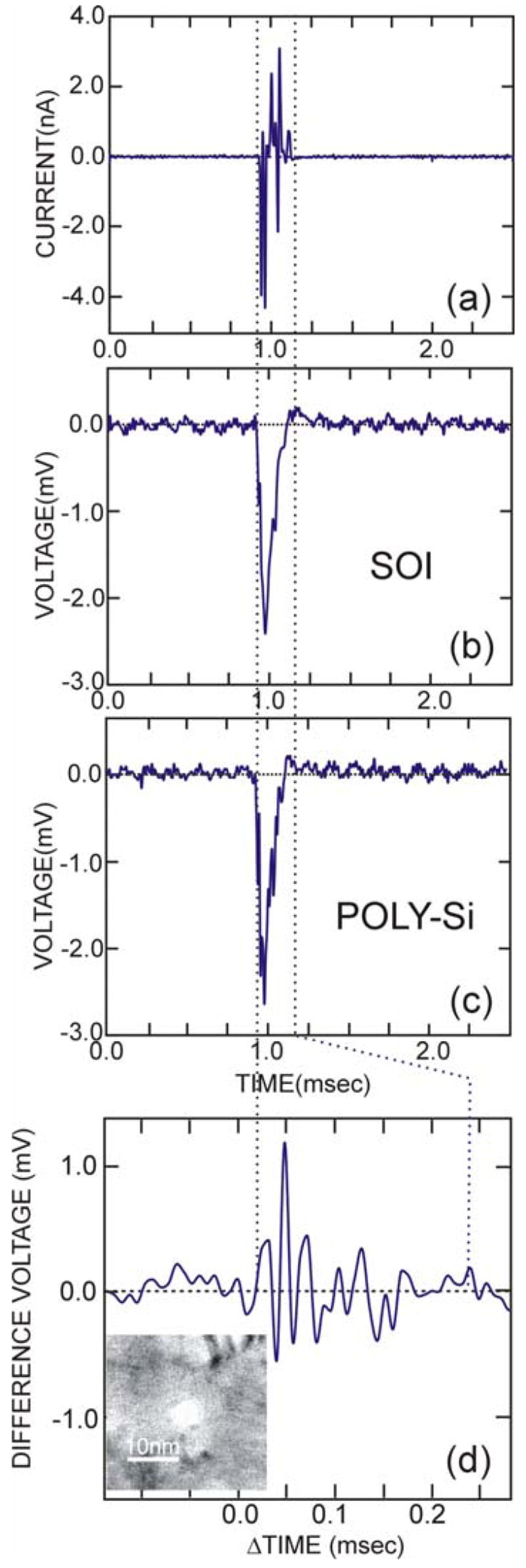
Corresponding to a transient in the current (a), we observe a voltage signature on the SOI and polysilicon electrodes (b) and (c) respectively. We attribute these signals to the translocation of a DNA through the pore. (d) shows the difference between the poly and SOI electrodes. A STEM image of the 7nm diameter pore is shown in an inset of (d). We attribute the fluctuations in the difference voltage to charge on the DNA.
We attribute these signals to the translocation of a single DNA molecule through the pore. These voltage signals represent the first measurement of a change in the potential across a nanopore due to the translocation of a molecule through it, but this sensor is not optimized for detecting the charge associated with a single nucleotide. Figure 8(d) represents the difference voltage measured between the SOI and polysilicon electrodes, showing a >1mV zero-to-peak signal level above a noise background of about 0.1mV-rms. Coincidently, this voltage corresponds with a simple estimate of the signal expected from the difference in the dipole moments of adenine(2.31D) 44,45 or thymine (4.44D) obtained by using: V=κ·pcosθ/r2, where κ=(4πεoεr)−1, εr is the relative permittivity of water in the pore ~10, p is the dipole moment, r~2.5nm is the distance to the electrode and θ~0° is the angle between the dipole and the pore axis. However, the narrow bandwidth of the voltage amplifier, the RC time constant τ~15μs (associated with the membrane capacitance of 15nF combined with the access resistance of approximately 1kΩ) the large diameter of the pore that permits an electrolytic current to flow while DNA translocates through it, all make it difficult to interpret the signal unequivocally. Measurements like these only indicate the feasibility of detecting the polarization associated with charge fluctuations in a DNA molecule.
Summary
In summary, synthetic nanometer-diameter pores can be fabricated easily (with sub-nanometer precision) in nanometer-thick, MOS-compatible membranes and used to detect DNA. The membranes are apparently mechanically robust and suitable for use at high voltage (~1V). Molecular dynamic simulations provide a means to both design a nanopore sensor for detecting the electronic signature associated with a particular molecule, and analyze the experimental outcomes. We have obtained preliminary data on a nanopore sensor implemented in a membrane fabricated from an MOS capacitor. Simulation of the operation of this sensor indicates that it may be possible to discriminate the charge associated with the translocation of a single nucleotide, under optimum conditions, but so far measurements of the voltage transient that develops during the translocation of 150bp dsDNA molecule have not resolved a nucleotide because of a 15–25μsec time constant and the large diameter of the pore.
Acknowledgments
We gratefully acknowledge frequent discussions with Jean-Pierre Leburton and Narayana Aluru in the Beckman Institute, and the use of the Center for Microanalysis of Materials supported by the US DOE Grant (DEFG02-91-ER45439). The authors thank Eduardo Cruz for Fig. 1(e). This work was funded by grants from NSF (0210843), the Air Force (FA9550-04-1-0214), and NIH (P41-RR05969). Computer time was provided through National Reources Allocation Committee grant MCA93S028.
Contributor Information
J. B Heng, Beckman Institute, University of Illinois, Urbana, IL.
A. Aksimentiev, Beckman Institute, University of Illinois, Urbana, IL
C. Ho, Beckman Institute, University of Illinois, Urbana, IL
V. Dimitrov, Beckman Institute, University of Illinois, Urbana, IL
T. Sorsch, New Jersey Nanotechnology Consortium, Murray Hill, NJ
J. Miner, New Jersey Nanotechnology Consortium, Murray Hill, NJ
W. Mansfield, New Jersey Nanotechnology Consortium, Murray Hill, NJ
K. Schulten, Beckman Institute, University of Illinois, Urbana, IL
G. Timp, Beckman Institute, University of Illinois, Urbana, IL
LITERATURE CITED
- 1. http://www.ncbi.nlm.nih.gov/projects/genome/guide/human/
- 2.Moore GE. IEEE IEDM Tech Dig. 1975:11–13. [Google Scholar]
- 3.Shendure J, Mitra RD, Varma C, Church GM. Advanced Sequencing technologies: Methods and Goals. Nature Review. 2004;5:335–344. doi: 10.1038/nrg1325. [DOI] [PubMed] [Google Scholar]
- 4. http://researchweb.watson.ibm.com/bluegene/
- 5.Salisbury MW. Fourteen sequencing innovations that could change the way you work. Genome Technol. 2003;35:40–47. [Google Scholar]
- 6.Paegel BM, Blazej RG, Mathies RA. Microfluidic devices for DNA sequencing: sample preparation and electrophoretic analysis. Curr Opin Biotechnolog. 2003;14:42–50. doi: 10.1016/s0958-1669(02)00004-6. [DOI] [PubMed] [Google Scholar]
- 7.Drmanac R, et al. DNA sequencing by hybridization with arrays of samples or probes. Methods Mol Biolo. 2001;170:173–179. doi: 10.1385/1-59259-234-1:173. [DOI] [PubMed] [Google Scholar]
- 8.Ronaghi M. Pyrosequencing sheds light on DNA sequencing. Geonme Res. 2001;11:3–11. doi: 10.1101/gr.11.1.3. [DOI] [PubMed] [Google Scholar]; Rudy B, Iverson LE, editors. Methods in Enzymology. Academic Press; 1992. [Google Scholar]
- 9.Benner S, et al. Gene expression analysis by massively parallel signature sequencing (MPSS) on microbead arrays. Nature Biotechnol. 2000;18:630–634. doi: 10.1038/76469. [DOI] [PubMed] [Google Scholar]
- 10.Braslavski I, Hebert B, Kartalov E, Quake SR. Sequence information can be obtained from single DNA molecules. PNAS. 2003;100(7):3960–3964. doi: 10.1073/pnas.0230489100. [DOI] [PMC free article] [PubMed] [Google Scholar]
- 11.Bayley H, Martin CR. Resistive-Pulse Sensing-From Microbes to Molecules. Chem Rev. 2000;100:2575–2594. doi: 10.1021/cr980099g. [DOI] [PubMed] [Google Scholar]
- 12.Deamer DW, Branton D. Characterization of Nucleic Acids by Nanopore Analysis. Acc Chem Res. 2002;35:817–825. doi: 10.1021/ar000138m. [DOI] [PubMed] [Google Scholar]
- 13.Akeson M, Branton D, Kasianowicz JJ, Brandin E, Deamer DW. Microsecond Time-Scale Discrimination Among Polycytidylic Acids, Polyadenylic Acid, and Polyuridylic Acid as Homopolymers or as Segments Within Single RNA Molecules. Biophysical J. 1999;77:3227–3233. doi: 10.1016/S0006-3495(99)77153-5. [DOI] [PMC free article] [PubMed] [Google Scholar]
- 14.Henrickson SE, Misakian M, Robertson B, Kasianowicz JJ. Driven DNA Transport into an Asymmetric Nanometer-Scale Pore. Phys Rev Lett. 2000;85(14):3057–3060. doi: 10.1103/PhysRevLett.85.3057. [DOI] [PubMed] [Google Scholar]
- 15.Kasianowicz JJ, Brandin E, Branton D, Deamer DW. Characterization of individual polynucleotide molecules using a memebrane channel. Proc Natl Acad Sci USA. 1996;93:13770–13773. doi: 10.1073/pnas.93.24.13770. [DOI] [PMC free article] [PubMed] [Google Scholar]
- 16.Kasianowicz JJ, Henrickson SE, Weetall HH, Robertson B. Simultaneous Multianalyte Detection with a Nanometer-Scale Pore. Anal Chem. 2001;73:2268–2272. doi: 10.1021/ac000958c. [DOI] [PubMed] [Google Scholar]
- 17.Meller A, Nivon L, Brandin E, Golovchenko J, Branton D. Rapid nanopore discimination between single polynucleotide molecules. P Natl Acad Sci USA. 2000;(3):1079–1084. doi: 10.1073/pnas.97.3.1079. [DOI] [PMC free article] [PubMed] [Google Scholar]
- 18.Vercoutere W, Winters-Hilt S, Olsen H, Deamer D, Haussier D, Akeson M. Rapid discrimination among individual DNA hairpin molecules at single-nucleotide resolution using an ion channel. Nature Biotechnology. 2001;19:248–252. doi: 10.1038/85696. [DOI] [PubMed] [Google Scholar]
- 19.Vercoutere WA, Winters-Hilt S, DeGuzman VS, Deamer D, Ridino SE, Rodgers JT, Olsen HE, Marziali A, Akeson M. Discrimination among individual Watson-Crick base pairs at the termini of single DNA hairpin molecules. Nucleic Acids Res. 2003;31 (4):1311–1318. doi: 10.1093/nar/gkg218. [DOI] [PMC free article] [PubMed] [Google Scholar]
- 20.Bayley H, Cremer PS. Stochastic sensors inspired by biology. Nature. 2001;413 (6852):226–230. doi: 10.1038/35093038. [DOI] [PubMed] [Google Scholar]
- 21.Kuhn K, et al. VLSI Tech Symp Tech Digest. 2004. p. 224. [Google Scholar]
- 22.Timp G, et al. Progress toward 10nm CMOS Devices. Proc IEDM. 1998:615–618. [Google Scholar]
- 23.Timp G, Bude J, Bourdelle KK, et al. The Ballistic Nanotransistor. Tech Digest IEDM. 1999:55–58. [Google Scholar]
- 24.Momose HS, Ohguro T, Morifuji E, Sugaya H, Nakamura S, Iwai H. Cutoff Frequency and Propagation Delay Time of 1.5-nm Gate Oxide CMOS. IEEE Trans Electron Dev. 2001;48(6):1165–1174. [Google Scholar]
- 25.Zandmer N, et al. VLSI Tech Symp Digest. 2004:98. [Google Scholar]
- 26.Dimitrov V, et al. High Performance, sub-50nm nMOSFET with 290-GHz fT for Mixed Signal Applications. Submitted to IEEE Trans Electron Dev 2005 [Google Scholar]
- 27.Suemitsu T, Enoki T, Yokoyama H, Ishii Y. Impact of two-step-recessed gate structure on RF performance of InP-based HEMTs. Electron Device Lett. 2004;34(2):220–222. [Google Scholar]
- 28.Khater M, et al. IEDM Technical Digest. 2004:549–552. [Google Scholar]
- 29.Hafez W, Feng M. 0.25μm emitter InP SHBTs with ft=550GHz. IEDM Technical Digest. 2004:247–250. [Google Scholar]
- 30.Hussian D, et al. IEDM Technical Digest. 2004:553–556. [Google Scholar]
- 31.Yu D, et al. IEDM Technical Digest. 2004:557–560. [Google Scholar]
- 32.Razavi B, Yan R, Lee KF. Impact of Distributed Gate Resistance on the Performance of MOS Devices, IEEE Trans Circuit and Systems-I: Fund. Theory and Appl. 1994;41(11):750–754. [Google Scholar]
- 33.Heng JB, Ho C, Kim T, Timp R, Aksimentiev A, Grinkova YV, Sligar S, Schulten K, Timp G. Sizing DNA using a Nanometer-diameter Pore. Biophysical Journal. 2004;87:2905–2911. doi: 10.1529/biophysj.104.041814. [DOI] [PMC free article] [PubMed] [Google Scholar]
- 34.Saenger Wolfram. Principles of Nucleic Acid Structure. Springer-Verlag; New York, Inc: 1984. [Google Scholar]
- 35.Cornell WD, et al. J Am Chem Soc. 1995;117:5179–5197. [Google Scholar]
- 36.Wendel, et al. J Chem Phys. 1992;97:5048–5062. [Google Scholar]
- 37.MacKerell AD, Jr, Brooks B, Brooks CL, Nilsson L, Roux B, Won Y, Karplus M. CHARMM: The energy function and its parameterization with an overview of the program. In: Schleyer P, et al., editors. The Encyclopedia of Computational Chemistry. John Wiley & Sons; Chichester: 1998. pp. 271–277. [Google Scholar]
- 38.Polygen. Quanta. Polygen Corporation; 200 Fifth Av., Waltham, MA 02254: 1988. [Google Scholar]
- 39.Aksimentiev A, Heng JB, Timp G, Schulten K. Microscopic Kinetics of DNA Translocation through Synthetic Pores. Biophysical Journal. 2004;87:2086–2097. doi: 10.1529/biophysj.104.042960. [DOI] [PMC free article] [PubMed] [Google Scholar]
- 40.Kong CY, Muthukumar M. Modeling of polynucleotide translocation through protein pores and nanotubes. Electrophoresis. 2002;23:2697–2703. doi: 10.1002/1522-2683(200208)23:16<2697::AID-ELPS2697>3.0.CO;2-M. [DOI] [PubMed] [Google Scholar]
- 41.Lubensky DK, Nelson DR. Driven Polymer Translocation Through a Narrow Pore. Biophysical J. 1999;77:1824–1838. doi: 10.1016/S0006-3495(99)77027-X. [DOI] [PMC free article] [PubMed] [Google Scholar]
- 42. ITRS Roadmap http://public.itrs.net/files/1999_SIA_Roadmap/Home.htm.
- 43.Hirose M, et al. Fundamental limit of gate oxide thickness scaling in an advanced MOSFET. Semicond Science and Tech. 2000;15(5):485. [Google Scholar]
- 44.Sponer J, Leszyzynski Jerzy, Hobza Pavel. Electronic Properties, Hydrogen Bonding, Stacking and Cation Binding of DNA and RNA bases. Biopolymers. 2002;61:3–31. doi: 10.1002/1097-0282(2001)61:1<3::AID-BIP10048>3.0.CO;2-4. [DOI] [PubMed] [Google Scholar]
- 45.Abraham RJ, Smith PE. Charge calculations in molecular mechanics 6: the calculation of partial atomic charges in nucleic acid bases and the electrostatic contribution to DNA base pairing. Nucleic Acids Res. 1988;16(6):2639–2657. doi: 10.1093/nar/16.6.2639. [DOI] [PMC free article] [PubMed] [Google Scholar]