

Abstract
We show that a semiconductor membrane made of two thin layers of opposite (n- and p-) doping can perform electrically tunable ion current rectification and filtering in a nanopore. Our model is based on the solution of the 3D Poisson equation for the electrostatic potential in a double-cone nanopore, combined with a transport model. It predicts that for appropriate biasing of the membrane-electrolyte system, transitions from ohmic behavior to sharp rectification with vanishing leakage current are achievable. Further more, ion current rectifying and filtering regimes of the nanopore correspond to different charge states in the p − n membrane which can be tuned with appropriate biasing of the n- and p- layers.
Keywords: ionic diode, doped semiconductor, surface charge, voltage, gated ion channels
Introduction
Proteinaceous nanopores have been studied for the last decade for their essential role in biology as nanoscale channels regulating the ion flow through cell membranes as well as exhibiting ion selectivity [1, 2]. Properties of the track-etched membranes have been studied in comparison to the properties of the various biological channels [3–5]. In the last few years, artificial nanopores in dielectric membranes etched by high energy ion or electron beams [6, 7] have been proposed as a substitute to biological ion channels [8–10]. However, such membranes are electrically insulating and do not provide tunable electrostatic control of the ion concentration inside or the ion flow through the nanopore. Recently, Karnik et al [11] experimentally demonstrated the metallic gate voltage modulation of ions and molecules concentration in a long channel with a nanoscale diameter to control the ionic conductance. Gold nanotubes with fully controlled ionic selectivity were reported in [12]. The ion selectivity was controlled by applying voltage to the tubes. Also, it was suggested that nanopores in n+ – Si membrane can be used as an ion filter by applying a voltage difference between the semiconductor and the electrolyte [13].
Similar to voltage-gated ion channels that belong to a class of transmembrane ion channels activated by changes in the electrical potential difference near the channel [1], the presence of a surface charge in a solid-state membrane is central for the use of nanopores in single molecule detection, ion/protein filtering [13] and potentially in DNA sequencing [14–16]. While the surface charge of biological channels can be positive, negative or spatially distributed in the pore to operate the “gating” mechanism interrupting the flow of molecules, water or ions [2], the surface charge in solid-state nanopores is usually negative and results from the fabrication process [14]. In this context, conical nanopores in polymer membranes with various (negative) surface charges have been investigated as ion rectifiers [17, 18]. Meanwhile, a microfluidic field effect transistor operating by surface charge modulation in an ion channel has been proposed [19] and theoretical modeling of ion transport in a nanofluidic diode and a bipolar transistor has been developed [20].
We have recently emphasized the versatility of semiconductor membranes in controlling the electrolyte charge in a nanopore [21]: unlike dielectric membranes that exhibit negative surface charges inducing positive ion charges at the nanopore surface, n-doped semiconductor membranes can attract either positive or negative ions at the nanopore surface, depending on the amount of positive dopant charge in the depletion layer of the n-type semiconductor. Moreover, the semiconductor membrane can be connected to a voltage source to modulate the nanopore channel charge.
In this letter, we propose to use membranes made of spatially separated n- and p-type doping layers (Fig. 1) to change the potential landscape in the channel and enhance the ionic conductance modulation. Indeed, advances in semiconductor technology has enable the fabrication of nanometer-scale layers with arbitrary n- or p- doping levels [22]. Hence, the existence of dipolar depletion charge at the surface of the membrane p − n junction induces a dipolar ionic charge in the nanopore, which is tunable by biasing electrically the homojunction which results in enhanced ionic filtering and rectifying properties compared with charged dielectric [17, 18] or mono-doped membranes [13].
FIG. 1.

(A) Geometry of the modeled nanopore in a solid-state membrane. The center X − Y cross-section is shown (the center Y − Z cross-section is similar). Two cuts S1 and S2 through the structure are indicated. S1 is taken at the center of the nanopore, while S2 is taken across the membrane, and is aligned with the pore axis. The drawing is not to scale. (B) Biological channel in a polarized membrane.
Membrane model
The nanopore-membrane structure geometry is shown schematically in Fig. 1, and consists of two 12nm Si layers of different doping: the top layer is n-doped (typically ) and the bottom layer is p-doped (typically ). The nanopore in this solid-state membrane has a double-conical shape with a 1nm diameter in the narrowest region and 6nm diameter opening on each side of the pore as a result of the electron beam fabrication process [14], but similar conclusions are expected for nanopores of more regular shape, e.g. cylindrical. The whole surface of the nanopore-membrane is covered by a 8 Å surface layer of SiO2 containing a fixed negative charge σ. The surface charge density was varied at first, but unless otherwise indicated the calculations are performed for σ = −0.0256C/m2. The membrane is immersed in an electrolyte KCl solution, with a concentration varying from 0.01M to 1M. Each material is characterized by its relative permittivity, i.e., εSi = 11.7, εSiO2 = 3.9. The dielectric constant of the electrolyte solution is chosen εelectrolyte = 78.
In order to obtain the ion charge distribution in the nanopore the Poisson equation is solved self-consistently by a multigrid method in the electrolyte-membrane system [23], assuming the ions in the electrolyte are fully dissociated and obey the Boltzmann distribution, whereas electrons and holes in the semiconductor are governed by the Fermi-Dirac statistics. The model details are described in [8, 21]. We use virtual solid-state parameters for the solution which enables us to formulate an all-semiconductor model for the charge and electric potential in the electrolyte and solid-state materials [24]. The electrolyte/solid state and semiconductor/oxide interfaces are modeled by introducing a conduction band offset between materials at their interfaces, i.e.: . We model the bias potential applied to the membrane with respect to the electrolyte by varying the quasi-Fermi levels of the Si n- (Vn) and p- (Vp) sides of the membrane separately over the −1V to 1V range.
3D electrostatic potential
Fig. 2A shows the potential variation (“build-in” potential) inside the membrane along cross-section S2 (Fig. 1A) for different densities of negative surface charges. No bias was applied to the membrane, so that there is no potential variation in the electrolyte far from the membrane, which was set to 0V for all studied electrolyte concentrations. The potential is positive on the n-side, and negative on the p-side of the membrane. Strong negative surface charges (σ3 and σ4) are manifested as two sharp drops in the potential profile at the top (y = 16 nm) and the bottom (y = 38 nm) surfaces of the membrane. Fig. 2B shows the potential variation in the nanopore along the pore axis (S1, Fig. 1A) for different densities of negative surface charges. Here, the potential maximum decreases and the potential minimum deepens as the negative surface charge density increases. Thus, strong negative surface charges (σ3 and σ4) fully offset the positive dopant charge on the n − Si side of the membrane at considered doping density. The increase of the doping density on the n-side of the membrane boosts the potential maximum on the n-side, whereas the potential minimum on the p-side shrinks (Fig. 2C). The increase of the doping density on the p-side results in the potential minimum enhancement (Fig. 2D).
FIG. 2.
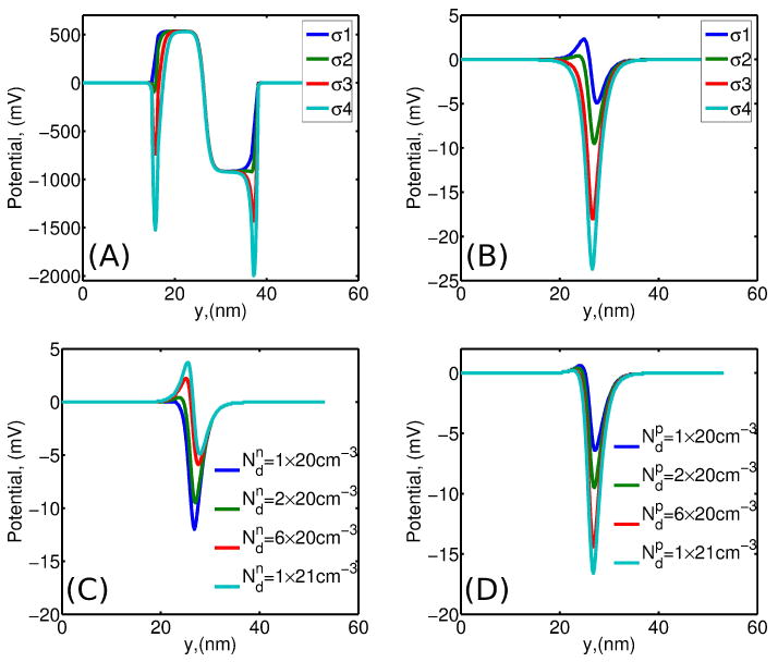
(A) Electrostatic potential across the membrane along S2 for difference surface charge densities σ1 = 0, σ2 = −0.0256C/m2, σ3 = −0.076C/m2 and σ4 = −0.128C/m2; (B) potential in the nanopore along S1 for the same charge densities as in (A); (C) potential in the nanopore along S1 for different n − Si side doping densities , with fixed doping density on the p − Si side of the membrane and surface charge density σ2; (D) potential in the nanopore along S1 for different p − Si side doping densities , with and σ2. Solution concentration is [KCl] = 1M in all cases.
Figs. 2C&D indicate that in order to obtain the maximum potential variation along the pore axis (condition that leads to the strongest current rectification), the doping density on both n – Si and p – Si sides of the membrane need to be maximized. Hence, the highest potential peak is achieved for the maximum doping density on the n- side (Fig. 2C), whereas on the p- side the deepest minimum is reached for the maximum doping density (Fig. 2D).
In Fig. 3 anion and cation concentrations at the nanopore center are shown for a solution concentration [KCl] = 0.1M for two membrane biases. The first case (n – Si biased at Vn = −1V, p – Si at Vp = 0V and electrolyte at V = 0V) is characterized by a single potential minimum in the pore, thus resulting in accumulation of cations in the nanopore center (Fig. 3A). The second case (n − Si at Vn = 1V, p − Si at Vp = 0V and electrolyte at V = 0V) gives rise to a potential profile with two extrema of opposite sign in the pore, which results in a dipolar ion charge in the pore: anions on the n − Si side, and cations on the p − Si side of the membrane (Fig. 3B).
FIG. 3.
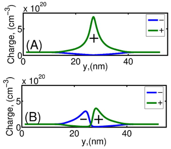
Anion (Cl−) and cation (K+) concentrations in the electrolyte solution in the nanopore center at S1 of a p − n membrane for two membrane biases: (A) Vn = −1V and Vp = 0V; and (B) Vn = 1V and Vp = 0V. Simulation parameters: σ = −0.0256C/m2, , , [KCl] = 0.1M.
The potential profiles for a range of membrane biases are displayed in Fig. 4(A-C) for a p − n membrane with typical material parameters, and [KCl] = 0.1M. For comparison, the potential profiles of a n − Si membrane with the same characteristics and a range of applied membrane biases are shown in Fig. 4(D). Unlike the electrostatic potential profile of the n − Si membrane that exhibits a single potential extremum i.e. either positive or negative, for all considered membrane biases, the potential along the channel in a p − n membrane produces either a single dominant maximum, a single dominant minimum or two extrema (one minimum and one maximum) as a function of applied bias between the n- and p- layers. This specificity of the p − n membrane to produce asymmetric potential landscape in the channel is directly related to the ionic current rectification properties of the nanopores as will be discussed in a later section.
FIG. 4.

(A-C) Electrostatic potential in the nanopore along S1 for [KCl] = 0.1M and surface charge density σ = −0.0256C/m2 for a p − n-membrane (doping densities are and ), for all solid lines Vp = −1V, for all dashed lines Vp = 1V: (A) Vn = −1V, (B) Vn = 0V, and (C) Vn = 1V. (D) Electrostatic potential in the nanopore for a n − Si membrane, , all other parameters are as in the p − n membrane case, for various applied to the membrane potential biases.
Let us point out that typical potential variations in the pore are ≳ 50mV (Fig. 4(A-C)), which is larger than the thermal voltage kT/e ≃ 25mV; one can expect larger variations at lower ion concentrations [KCl] < 0.1M due to reduced screening of the nanopore walls by ions, and consequently improved selectivity and rectification function.
Current-voltage characteristics
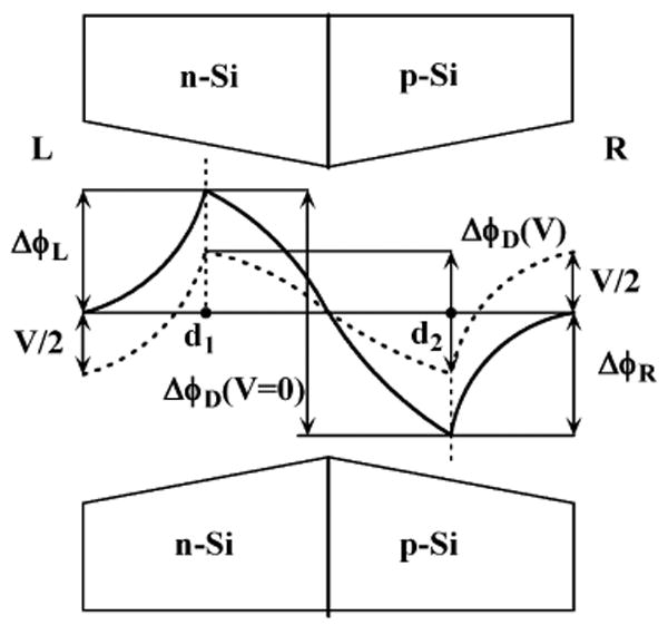
In order to calculate the current-voltage characteristics of the electrolyte as a function of the potential landscape in the nanopore, we develop an electrodiffusion model for ionic transport similar to [25]. Fig. 5 shows a schematic profile of the potential with two extrema of opposite signs in the pore along the S1 cross-section. The external and internal pore solution concentrations are connected through the following Donnan equilibrium conditions [26]:
FIG. 5.
Sketch of the nanopore in a p − n membrane with one of the possible electrostatic potential variations in the nanopore. Positive current flows from the left to the right.
| (1) |
| (2) |
where zi is the charge number of species i. ci,L and ci,R denote species i concentration of electrolyte solution on the left and the right of the nanopore, correspondingly. Similar notation is used for the potential φ: φL and φR are potentials on the left and on the right side of the membrane (they are equal when no driving bias is applied), whereas φ(d1) and φ(d2) are potentials at the coordinates x = d1 and x = d2 inside the pore, correspondingly. ΔφL = φ(d1) − φL and ΔφR = φR − φ(d2) are the Donnan potential drops through the left and right interfaces, respectively, and ΔφD = φ(d2) − φ(d1) is the diffusion potential in the pore. The potential differences ΔφL, ΔφD and ΔφR are determined directly from the calculated potential profiles in the nanopore.
We assume that the flux Ji of species i through the nanopore is described by the Nernst-Planck equations
| (3) |
where Di is the diffusion coefficient of species i in the pore solution, and constants F, R and T have their usual meaning [26]. The total electrical current I passing through the nanopore under the applied electrolyte bias V = φL − φR (see potential profile in Fig. 5 as dashed line between the two sides of the membrane) is given by
| (4) |
and the bias potential difference applied to the system can be written
| (5) |
Eqs (3,4,5) with boundary conditions (1,2) allow us to obtain analytical expressions of ionic fluxes if we consider the constant field approximation between coordinates x = d1 and x = d2:
| (6) |
By assuming that the potential drops ΔφL and ΔφR at the left and right interface do not change with applied bias, as in biological channels [26], the I − V characteristics can be obtained by substituting ΔφD(V) = ΔφD(V = 0) − V in the right hand side of Eq (6) with cS,L = cS,R = c0 = 0.01M on each side of the membrane; we use DK+ = 1.95 × 10⁻⁵cm2/s, DCl− = 2.03 × 10⁻⁵cm2/s for the diffusion coefficients of potassium and chlorine ions. Once the total electrical current is calculated, the nanopore conductance G = dI/dV and the ion selectivity in the nanopore are readily obtained.
Ion current rectification and filtering
Fig. 6(A-F) left column shows the electrostatic potential profiles in the nanopore for [KCl] = 0.01M at different biases between the n − Si and p − Si sides of the semiconductor membrane at electrolyte bias V = 0. The membrane potential biases Vn(p) vary from −1V to 1V with respect to the electrolyte. For this low molar [KCl] concentration the potential variations in the nanopore are dramatic with up to 200mV swing magnitude. The corresponding positive and negative charge distribution as well as current-voltage characteristics are shown in Fig. 6(A-F) center and right column, correspondingly. It is seen that, as a function of the voltage across the p − n membrane, the I − V characteristics behavior varies from quasi-ohmic (i.e. Fig. 6C right column with Vn = −0.5V, Vp = 1V) to diode-like with vanishing leakage current at V > 0 (i.e. Fig. 6F right column with Vn = 1V, Vp = 0V). In our configuration, the ohmic behavior with the largest conductance is attributed to a potential profile with a single minimum of weak amplitude in the nanopore (Fig. 6C), while the sharpest diode-like characteristic corresponds to an antisymmetric sine-like potential profile of large amplitude (Fig. 6F). All intermediate potential profiles result in asymmetric I − V characteristics for which the conductance at V < 0 is always larger than the conductance at positive electrolyte bias V > 0. The closer the potential profile to a sine-like shape, the better the rectification. The lower the potential amplitude, the closer the ohmic behavior. Correspondingly, the more symmetric the charge distribution with respect to the nanopore center, the “more ohmic” the current (Fig. 6A,B,C). Alternatively, the more asymmetric the charge distribution, the more rectified the current (Fig. 6D,E,F). The fact that the high conductance regime is at negative electrolyte bias is due to the p − n membrane configuration for which the n-layer is on the same side as the positive solution electrode.
FIG. 6.
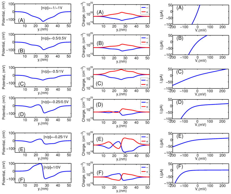
(Left, A-F) Electrostatic potential in the nanopore along cross-section S1 for various membrane biases. [KCl] = 0:01M and surface charge density σ = −0.0256C/m2 for p – n- membrane (doping densities are , and ). Electrolyte bias V=0. Membrane n- and p- layer bias potentials are indicated in legend as [n/p]. (Center, A-F) Positive and negative charge distributions in the nanopore along cross-section S1 for the same p – n-membrane biases. Note the log scale. (Right, A-F) Current-voltage characteristics calculated for the same p – n-membrane biases.
In Fig. 7A we plot the ion selectivity S of the nanopore as a function of δ = ΔφL − ΔφR at different membrane p- and n- layer biases. We observe that the selectivity S ≈ 0 when δ = 0 which corresponds to an antisymmetric (sine-like) shape potential (rectification condition) (Fig. 5) whereas the selectivity increases with the absolute value of δ, and even reaches S ≈ 1 for δ = −200mV (conditions far from rectification). Fig. 7B shows the relative ionic conductance GCl/GK plotted in log scale as a function of δ. It can be seen that the relative conductance increases exponentially with δ, which is consistent with the flux expression (Eq (6)). The low selectivity regime with δ ≈ 0 corresponds to a relative conductance close to unity. The left hand sides of both Figs. 7A,B with δ < 0 correspond to high selectivity and high conductance for positive K+ ions since GCl/GK ≪ 0, while the right hand sides of the Figs. 7A,B plots with δ > 0 correspond to high selectivity and high conductance for negative Cl− ions since GCl/GK ≫ 0.
FIG. 7.

(A) Ion selectivity. (B) Ion conductance ratio. All of the above calculated for the electrostatic potentials presented in Fig. 6 for the same system parameters.
To summarize, the membranes under biases which result in nanopore potentials with double extrema of equal height lead to the low selectivity regime (i.e. Vn = 1V, Vp = 0V). Alternatively, the nanopore potentials with a single extrema result in the high selectivity regime, with a single potential minimum is being selective towards positive (K+) ions (i.e. Vn = −1V, Vp = −1), whereas a large potential maximum is being selective towards negative (Cl−) ions (i.e. Vn = 1V, Vp = 1V).
Therefore, one concludes that current rectification and filtering are two different regimes corresponding to two different charge states of the p − n membrane, which can be tuned by electrically biasing the p − n layers. More generally, the p − n membrane can be used for separation of charged species, controlled injection, release and blockade of charged molecules and ions, thereby mimicing in a very basic way the operation of voltage gated biological channels in cells. The p − n nanopore device also provides an opportunity to trap, stretch and effectively slow down DNA translocation in the pore, thus rising the resolution of the proposed nanopore sequencing device [8, 9].
Conclusions
It is well known that any biological channel in a cell membrane needs to be electrically asymmetric with respect to the membrane plane to perform some form of selectivity or rectification. Similarly, any artificial nanopore with asymmetric electrical potential profile (whether it comes from asymmetry in pore geometry, surface charge distribution, or both) in a nanopore will produce ion current rectification through the pore with applied electrolyte bias. In this work we showed that unlike conical nanopores with predefined rectifying properties [17, 27], nanopore in a p − n membrane can be tuned electrically from ohmic behavior to any desirable rectification, and to a complete blockade of the total ionic current without the need for buffer solution replacement or membrane treatment. Simultaneously, it can perform as ion filter with the possibility to filter ions of either sign.
We note that at the time of completion of this manuscript Vlassiouk & Siwy and Karnik et al. [28, 29] discussed the use of single nanopores decorated with fixed local positive charges as a nanofluidic “diode” and ion current rectifier. While these configurations provide rectification, additional flexibility can be obtained via manipulation of the solution pH once the surface charge is deposited or via chemical modification of the membrane to invert the I-V curves. With semiconductor membranes it is also possible to add another n or p layer to create n − p − n or p − n − p structures that will allow control over the ionic flow in both directions, and this will be the topic of a forthcoming publication [30].
Acknowledgments
This work was funded by NIH grant ROI-HG003713-01. The authors gratefully acknowledge the use of the supercomputer time at the National Center for Supercomputer Applications.
References
- 1.Alberts B, Bray D, Johnson A, Lewis J, Raff M, Roberts K, Walter P. Essential Cell Biology. Garland; 1998. [Google Scholar]
- 2.Beckstein O, Sansom M. Phys Biol. 2004;1:42–52. doi: 10.1088/1478-3967/1/1/005. [DOI] [PubMed] [Google Scholar]
- 3.Korchev YE, Bashford CL, Alder GM, Apel PY, Edmonds DT, Lev AA, Nandi K, Zima AV, Pasternak CA. FASEB J. 1997;11(7):600–608. doi: 10.1096/fasebj.11.7.9212084. [DOI] [PubMed] [Google Scholar]
- 4.Lev AA, Korchev YE, Rostovtseva TK, Bashford CL, Edmonds DT, Pasternak CA. Proc Biol Sci. 1993;252(1335):187–192. doi: 10.1098/rspb.1993.0064. [DOI] [PubMed] [Google Scholar]
- 5.Bashford CL, Alder GM, Pasternak CA. Biophys J. 2004;82:2032–2040. doi: 10.1016/S0006-3495(02)75551-3. [DOI] [PMC free article] [PubMed] [Google Scholar]
- 6.Li J, Stein D, McMullan C, Branton D, Aziz MJ, Golovchenko JA. Nature. 2001;412:166–169. doi: 10.1038/35084037. [DOI] [PubMed] [Google Scholar]
- 7.Storm AJ, Chen JH, Ling XS, Zandbergen HW, Dekker C. Nature Materials. 2003;2:537–540. doi: 10.1038/nmat941. [DOI] [PubMed] [Google Scholar]
- 8.Gracheva ME, Xiong A, Aksimentiev A, Schulten K, Timp G, Leburton JP. Nanotechnology. 2006;17:622–633. [Google Scholar]
- 9.Heng JB, Ho C, Kim T, Timp R, Aksimentiev A, Grinkova YV, Sligar S, Schulten K, Timp G. Biophys J. 2004;87:2905–2911. doi: 10.1529/biophysj.104.041814. [DOI] [PMC free article] [PubMed] [Google Scholar]
- 10.Kasianowicz JJ, Brandin E, Branton D, Deamer DW. PNAS USA. 1996;93:13770–13773. doi: 10.1073/pnas.93.24.13770. [DOI] [PMC free article] [PubMed] [Google Scholar]
- 11.Karnik R, Fan R, Yue M, Li D, Yang P, Majumdar A. Nano Lett. 2005;5:943–948. doi: 10.1021/nl050493b. [DOI] [PubMed] [Google Scholar]
- 12.Nishizawa M, Menon VP, Martin CR. Science. 1995;268:700–702. doi: 10.1126/science.268.5211.700. [DOI] [PubMed] [Google Scholar]
- 13.Vidal J, Gracheva ME, Leburton JP. Nanoscale Res Lett. 2007;2:61–68. [Google Scholar]
- 14.Ho C, Qiao R, Heng JB, Chatterjee A, Timp RJ, Aluru NR, Timp G. PNAS. 2005;102:10445–10450. doi: 10.1073/pnas.0500796102. [DOI] [PMC free article] [PubMed] [Google Scholar]
- 15.Fologea D, Uplinger J, Thomas B, McNabb DS, Li J. Nano Lett. 2005;5:1734–1737. doi: 10.1021/nl051063o. [DOI] [PMC free article] [PubMed] [Google Scholar]
- 16.Fan R, Karnik R, Yue M, Li D, Majumdar A, Yang P. Nano Lett. 2005;5:1633–1637. doi: 10.1021/nl0509677. [DOI] [PubMed] [Google Scholar]
- 17.Siwy Z, Heins E, Harrell C, Kohli P, Martin C. J Am Chem Soc. 2004;126:10850–10851. doi: 10.1021/ja047675c. [DOI] [PubMed] [Google Scholar]
- 18.Cervera J, Schiedt B, Neumann R, Mafá S, Ramírez P. J of Chem Phys. 2006;124:104706. doi: 10.1063/1.2179797. [DOI] [PubMed] [Google Scholar]
- 19.Horiuchi P, Dutta P. Lab chip. 2006;6:714–723. doi: 10.1039/b600067c. [DOI] [PubMed] [Google Scholar]
- 20.Daiguji H, Oka Y, Shirono K. Nano Lett. 2005;11:2274–2280. doi: 10.1021/nl051646y. [DOI] [PubMed] [Google Scholar]
- 21.Gracheva ME, Leburton JP. Nanotechnology. 2007;18:145704–145710. [Google Scholar]
- 22.Dimitrov V, Aksimentiev A, Schulten K, Heng J, Sorsch T, Mansfield W, Miner J, Watson GP, Cirelli R, Klemens F, Bower J, Ferry E, Taylor A, Kornblit A, Dorvel B, Zhao Q, Timp G. Exploring the Prospects for a Nanometer-scale Gene Chip. IEDM Tech Digest. 2006:169–173. [Google Scholar]
- 23.Press WH, Teukolsky SA, Vetterling WT, Flannery BP. Numerical Recipes in Fortran 77. Cambridge University Press; 2001. On-line: http://www.nr.com. [Google Scholar]
- 24.Gardner CL, Nonner W, Eisenberg RS. J of Comp Elect. 2004;3:25–31. [Google Scholar]
- 25.Ramírez P, Mafé S, Aguilella VM, Alcaraz A. Phys Rev E. 2003;68:011910(1)–011910(8). doi: 10.1103/PhysRevE.68.011910. [DOI] [PubMed] [Google Scholar]
- 26.Lakshminarayanaiah N. Equations of membrane biophysics. Academic; New York: 1984. [Google Scholar]
- 27.Siwy Z. Adv Funct Mater. 2006;16:735–746. [Google Scholar]
- 28.Vlassiouk I, Siwy ZS. Nano Lett. 2007;7:552–556. doi: 10.1021/nl062924b. [DOI] [PubMed] [Google Scholar]
- 29.Karnik R, Duan C, Castelino K, Daiguji H, Majumdar A. Nano Lett. 2007;7:547–551. doi: 10.1021/nl062806o. [DOI] [PubMed] [Google Scholar]
- 30.Gracheva ME, Leburton JP. 2007 to be published. [Google Scholar]