Abstract
We report the nanocluster-catalyzed growth of ultra-long and highly-uniform single-crystalline silicon nanowires (SiNWs) with millimeter-scale lengths and aspect ratios up to ca. 100,000. The average SiNW growth rate using disilane (Si2H6) at 400 °C was 31 µm/min, while the growth rate determined for silane (SiH4) reactant under similar growth conditions was 130 times lower. Transmission electron microscopy studies of millimeter-long SiNWs with diameters of 20–80 nm show that the nanowires grow preferentially along the <110> direction independent of diameter. In addition, ultra-long SiNWs were used as building blocks to fabricate one-dimensional arrays of field-effect transistors (FETs) consisting of ca. 100 independent devices per nanowire. Significantly, electrical transport measurements demonstrated that the millimeter-long SiNWs had uniform electrical properties along the entire length of wires, and each device can behave as a reliable FET with an on-state current, threshold voltage, and transconductance values (average ± 1 standard deviation) of 1.8 ± 0.3 µA, 6.0 ± 1.1 V, 210 ± 60 nS, respectively. Electronically-uniform millimeter-long SiNWs were also functionalized with monoclonal antibody receptors, and used to demonstrate multiplexed detection of cancer marker proteins with a single nanowire. The synthesis of structurally- and electronically-uniform ultra-long SiNWs may open up new opportunities for integrated nanoelectronics, and could serve as unique building blocks linking integrated structures from the nanometer through millimeter length scales.
Semiconducting nanowires (NWs)1–5 are attractive building blocks for fabricating functional nanodevices with single device demonstrations reported for field-effect transistors (FETs),6 memories,7 light emitting diodes,8 laser diodes,9 and biological sensors.10 More complex device arrays and simple circuits, including logic gates,11 ring oscillators,12 and multiplexed biosensors13 have been demonstrated by interconnection of multi-NW devices. A complementary approach for device integration would be to employ ultra-long NWs with multiple devices on a single NW, assuming that materials with uniform structure and electronic properties could be prepared. Ultra-long nanowires could also benefit overall integration by facilitating interconnection of nanoelectronic device arrays, which are defined on single NWs, to larger scale input/output wires in a system.
Previously, millimeter-long SiNWs14 with a range of structural properties have been produced by high-temperature thermal evaporation of silicon monoxide14a and silicon14b powders; however, the electronic properties and nanoelectronic device characteristics have not been reported. The nanocluster-catalyzed vapor-liquid-solid (VLS) growth method is a promising method for the growth of single-crystal NWs with controlled diameter, length and electronic properties.1–4 The kinetics of SiNW VLS growth have been studied recently by several groups.15,16 Interestingly, diameter-independent15 and diameter-dependent16 growth rates have been observed, although in all cases the rates have been slower than 1–2 µm/min.17 These reported rates make the VLS-based growth of millimeter length SiNWs a significant challenge. We note that much larger micrometer-scale diameter Si whiskers have exhibited growth rates reaching ~1 µm/sec,18 which would facilitate growth of millimeter length structures.
To investigate nanocluster-catalyzed VLS synthesis of millimeter-long single-crystal SiNWs, we have considered whether the overall growth rate could be increased by accelerating the rate-limiting step in the process.15,16,19,20 The overall growth process can be broken down into contributions from (i) catalytic adsorption of gaseous reactants at the surface of liquid nanoparticles, (ii) diffusion of Si through the liquid alloy to a sink, and (iii) crystallization at liquid-solid interface.2,16,19,21 The critical importance of steps (i) and/or (iii) in limiting growth rate has been discussed.15,16,19,20 Our previous studies have shown that single-crystal SiNWs synthesized via gold nanocluster-catalyzed VLS growth proceeds with growth rates of ca. 1 µm/min using silane (SiH4) as gas-phase recactant.17,22 The strong temperature dependence of the SiNW growth rate under optimized conditions suggests that SiH4 decomposition kinetics are more important than the gas-phase mass transport,23 and thus that acceleration of the decomposition step might enhance the observed growth rate. Here we explore SiNW growth using disilane (Si2H6) since Si2H6 is expected to have a higher catalytic decomposition rate due to lower activation energy for cleavage of Si-Si versus Si-H bonds.24
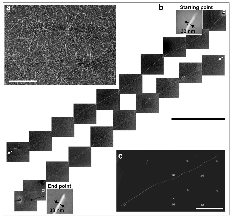
SiNWs were synthesized at 390–410 °C using gold nanoclusters as catalysts and Si2H6 (3 sccm) as reactant source25 with other procedures similar to our previous reports for SiH4-based SiNW growth.4,17,22,26 Scanning electron microscopy (SEM) images of the growth wafer (Figure 1a) show the presence of very long nanowires with varying degrees of entanglement. The long SiNWs were transferred to clean substrates via a reported shear contact printing process,27which can extend and align the SiNWs for direct and unambiguous length measurements. Analysis of a series of 20 scanning SEM images recorded along the length of a representative ultra-long SiNW (Figure 1b) demonstrate several important points. First, the length of the ca. 30 nm diameter nanowire, 2.3 mm, is almost 100-times longer than the SiNWs we typically produce using SiH4 reactant. The entire SiNW can also be readily visualized in dark-field optical microscopy images as shown in Figure 1c. Second, the NW diameter is very uniform with the starting and end points of ca. 31 nm and 33 nm, respectively. This uniform diameter indicates (i) that there is little or no homogeneous deposition of Si2H6 on the elongating nanowire during the synthesis26 and (ii) that Au from the catalyst does not incorporate into or diffuse along the surface to a substantial amount during growth. Third, quantitative analysis of the lengths of ultra-long SiNWs produced following 1-hour growth yielded an average of 1.8 mm with longest NWs at or exceeding 3.5 mm.
Figure 1.
(a) SEM image of as-grown ultra-long SiNWs synthesized by Si2H6 at 400 °C for 30 min. Scale bar, 20 µm. (b) A series of 20 SEM images of a 2.3-mm-long SiNW transferred on SiO2/Si substrate. Scale bar, 200 µm. Insets, SEM images of starting and end segments of this NW. (c) Dark-field optical image of the same wire. Scale bar, 500 µm.
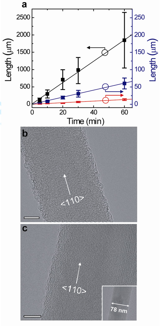
We have compared SiNW growth rates using Si2H6 versus SiH4 with other conditions fixed except growth temperature in order to probe the origin of the faster growth rates leading to the ultra-long SiNWs. Plots of the SiNW length versus growth time with Si2H6 at 400 °C, SiH4 at 400 °C, and SiH4 at 450 °C for 30 nm diameter NWs (Figure 2a) show that the average growth rate for Si2H6 at 400 °C is ca. 31 µm/min, which is ca. 130 times higher than that for SiH4 at the same temperature (0.24 µm/min) and 31 times higher than for SiH4 at our optimal growth temperature of 450 °C (1.0 µm/min). Using the temperature-dependent gas phase decomposition rate data for Si2H6 and SiH4 24 we estimate Si2H6 (400 °C) : SiH4 (400 and 450 °C) of approximately 170 and 10, respectively. These values are similar to the experimental ratios of growth rates, and thus suggest that reactant decomposition kinetics is important in determining the observed SiNW growth rates.
Figure 2.
(a) Plot of SiNW length versus growth time for Si2H6 at 400 °C (black), SiH4 at 400 °C (red) and SiH4 450 °C (blue). (b) Lattice-resolved TEM image recorded along <111> zone axis of a 18 nm diameter ultra-long SiNW; scale bar is 5 nm. (c) Lattice-resolved TEM image of a 78 nm diameter ultra-long SiNW; scale bar is 5 nm. Inset is a lower magnification image of the SiNW.
The structural characteristics of the ultra-long SiNWs were also investigated by transmission electron microscopy (TEM). Lattice-resolved images of an ca. 18 nm diameter SiNW (Figure 2b) shows that that the SiNW is a single-crystalline structure despite the fact that growth occurred at rates at least 10x greater than previous studies.4,15–17,19,22 The TEM image and two-dimensional Fourier transform analysis (Figure S1a) further demonstrated that the growth axis was <110>, consistent with previous studies of smaller diameter SiNWs.4,22 In addition, TEM studies of 18 SiNWs with diameters from 15 to 80 nm (Figure 2c and Figure S1b) all showed single-crystalline structures with a growth axis of <110> independent of diameter, where 13/18 of the sampled SiNWs had diameters between 29 to 80 nm. Interestingly, the diameter-independent growth direction observed for the ultra-long SiNWs contrasts previous studies where a cross-over to <111> direction at approximately 20 nm was observed.4,5,22
Previously, Schmidt et al.5 proposed a model based on the free energy, which is influenced by the interplay of the liquid-solid interfacial tension with Si surface edge tension, to explain consistently diameter dependent growth in SiNWs. Within the context of this model, a larger critical cross-over diameter from <110> to <111> would be observed for an interfacial thickness that increased with crystallization rate. We speculate that the faster growth rates used to achieve the ultra-long SiNWs might lead to an increase of the interfacial thickness parameter, although future studies of critical diameter versus growth rate will be required to clarify this point. Regardless of the detailed origin, we believe these observations suggest that it will be interesting to explore and possibly exploit kinetic effects as a means to controlling growth directions for NWs produced by the nanocluster-catalyzed VLS process.
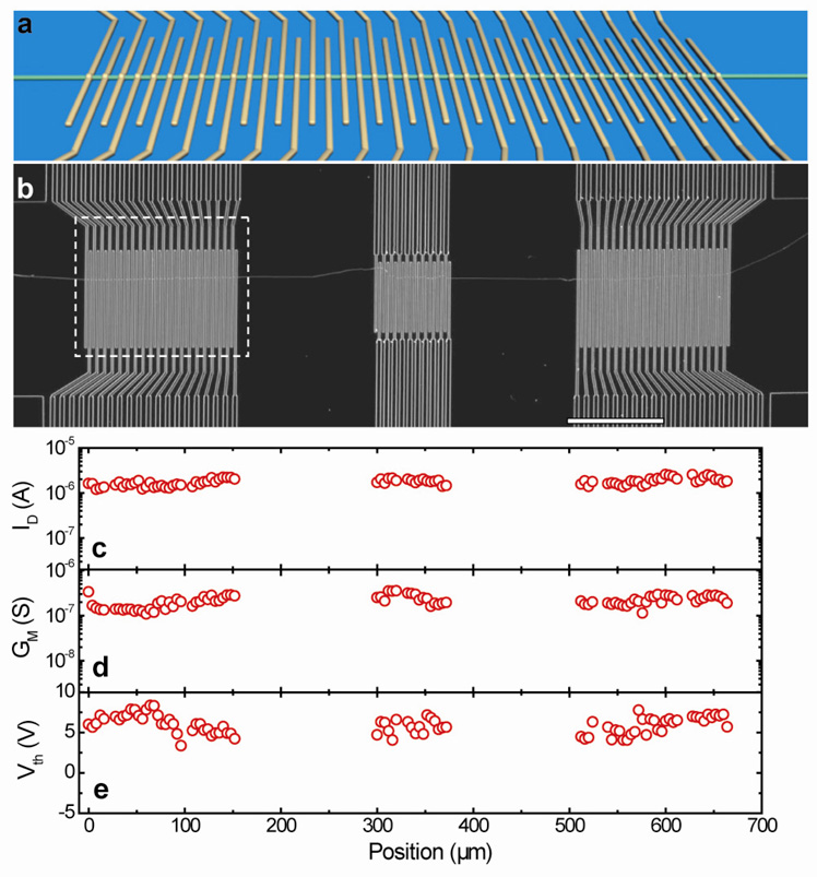
The ultra-long SiNWs represent potentially attractive building blocks for nanoelectronics because it would be possible to define a large number of devices on a single NW, thus facilitating integration as shown schematically in Figure 3a. In addition, the fabrication and characterization of multiple devices on a single NW could provide important information addressing doping and electronic uniformity of these nanostructures. To address these issues we have prepared ultra-long boron-doped SiNWs, 25 aligned the NWs on substrate by shear contact printing,27 and defined arrays of FETs by electron beam lithography.10a,11,26,28 A representative optical image (Figure 3b) highlights the large number of addressable FETs defined on the ultra-long SiNWs.
Figure 3.
(a) Schematic of multiple FET array on a single ultra-long p-SiNW. (b) Dark-field optical image of multiple FETs defined by electron beam lithography. The p-SiNW is horizontal in the image and the vertical lines crossing the NW correspond to S/D electrodes with 2 µm width/2 µm separation; scale bar is 100 µm. The dashed white rectangle corresponds to a similar area shown schematically in (a). (c) Position vs. ID at VD= 1V and VG = −10 V measured from the multiple FETs defined on the single p-SiNW in the image. (d) Position vs. GM at VD = 1V. (e) Position vs. Vth.
Electrical transport measurements showed that more than 90% devices behaved as good p-type devices. Specifically, source-drain current (ID) versus source-drain voltage (VD) curves at small VD were linear, which demonstrates good contacts across the NW. The decrease in ID with increasingly positive VG (Figure S2) also showed that devices were p-type depletion mode FETs. In addition, we have assessed and compared quantitatively key transistor characteristics, including on-state current, Ion, peak transconductance, GM, and threshold voltage, Vth, as a function of position across the single SiNW array. Notably, the Ion (Figure 3c), GM (Figure 3d) and Vth (Figure 3e) show very reproducible values across the entire array spanning almost 1 mm in length with average ± 1 standard deviation values of 1.77 ± 0.33 µA, 213 ± 61 nS/V and 6.0 ± 1.1 V, respectively. Previous studies of individual nanowire FETs6a,29 have exhibited larger variations in key FET properties, with variations in threshold voltage of 35–135 versus ~20% and transconductance of 58–76% versus ~30%. This comparison indicates that the ultra-long SiNWs are electrically homogeneous and yield device reproducibility higher than achieved from single NW-based FETs. Last, these measurements also suggest that the active boron dopant yielding the p-type behavior must be incorporated in a uniform manner during nanocluster-catalyzed VLS growth.
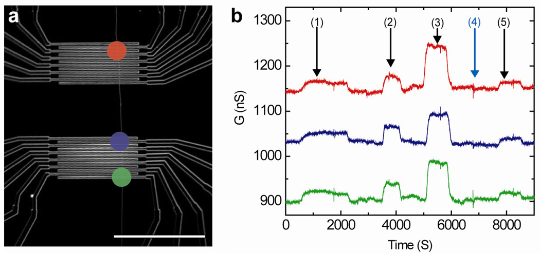
The ability to define large numbers of functional FETs along single ultra-long NWs can open up new opportunities for integrated nanoelectronics. To demonstrate this concept we have explored multiplexed protein detection using monoclonal antibody (mAb) functionalized SiNW FETs (Figure 4a). In previous studies,13 we have demonstrated multiplexed detection using mAb functionalized devices, but in this case each device was from an individual SiNW thus necessitating well-defined assembly to achieve the FET array. Demonstration of multiplexed measurements from independently addressable FETs defined on a single ultra-long SiNW has not been previously achieved using either nanowires or carbon nanotubes. However, this approach could have substantial impact on the biosensor area10a,13 because (i) it simplifies fabrication of multiplexed sensor device arrays, and (ii) given the greater device homogeneity for FETs defined on a single ultra-long SiNW opens up the opportunity to assess sensing reproducibility in device arrays where device-to-device variability should not be the dominating factor.
Figure 4.
(a) Optical image of a multiple sensor array with similar source-drain dimensions as in Figure 3b; scale bar, 100 µm. The red, blue and green circles highlight regions from which sensing data were recorded. (b) Conductance-versus-time data measured simultaneously from three FET devices from the red, blue and red regions of the device array. The SiNW FET array was functionalized with mAb for PSA, and the data were recorded by alternating delivery of target solutions (PSA or BSA) and buffer solution where vertical arrows correspond to the delivery of (1) 20 pg/ml PSA, (2) 500 pg/ml PSA, (3) 10 ng/ml PSA, (4) 10 µg/ml BSA, and (5) 20 pg/ml PSA solutions. The functionalization and measurement procedures were the same as reported previously.13,17
Conductance versus time data recorded from three distinct FETs defined on the single ultra-long SiNW, which was functionalized uniformly with the mAb for prostate specific antigen (PSA), showed several key features. First, the devices exhibited well-defined and reversible conductance increases associated with the binding and unbinding of the specific target PSA. Second, the conductance change was proportional to the PSA concentration, as expected for equilibrium binding response. Third, the concentration-dependent conductance change recorded in the distinct FET elements, which were separated by >100 µm, was similar and testifies to the electronic uniformity of the ultra-long SiNWs and the uniform mAb functionalization. Fourth, we note that addition bovine serum albumin at 1000x higher concentration showed no response, demonstrating good selectivity.13 Last, the reproducible conductance change from each of the addressable devices is consistent with the homogeneous device characteristics demonstrated in above in Figure 3. While the present measurements represent a relatively simple demonstration of multiplex protein detection, they do demonstrate a new approach for multiplexing that could be extended in the future to include parallel, real-time measurements from a larger number of devices functionalized with diverse mAb receptors.
In summary, we have demonstrated the nanocluster-catalyzed growth of millimeter-long and highly-uniform single-crystalline SiNWs with aspect ratios up to ca. 100,000. The average SiNW growth rates using Si2H6 reactant were 30–130 times faster than previous rates observed using SiH4 reactant under similar growth conditions. TEM studies showed that the ultra-long SiNWs grow preferentially along the <110> direction independent of diameter, and suggest that kinetic effects may be used as a means for controlling growth directions in NWs produced by the nanocluster-catalyzed VLS process. In addition, ultra-long SiNWs were used as building blocks to fabricate one-dimensional FET arrays that exhibit high-degree of device uniformity over millimeter dimensions, and testify to the electrical/doping homogeneity of SiNWs produced by nanocluster-catalyzed VLS growth. Lastly, the uniform device properties of one-dimensional FET arrays were exploited to demonstrate a new approach to multiplexed detection of cancer marker proteins with a single nanowire. The synthesis of structurally- and electronically-uniform ultra-long SiNWs may open up new opportunities for integrated nanoelectronics, and could serve as unique building blocks linking integrated structures from the nanometer through millimeter length scales.
Supplementary Material
Acknowledgment
We thank J. Xiang for helpful discussion. W.I.P acknowledges support from the Korea Research Foundation Grant funded by the Korean Government (MOEHRD, Basic Research Promotion Fund) (KRF-2007-331-D00194). C.M.L. acknowledges support of this work through a contract from National Institutes of Health, MITRE Corporation, and Samsung Electronics.
References
- 1.Morales A, Lieber CM. Science. 1998;279:208. doi: 10.1126/science.279.5348.208. [DOI] [PubMed] [Google Scholar]
- 2.(a) Lieber CM, Wang ZL. MRS Bull. 2007;32:99. [Google Scholar]; (b) Xia Y, Yang P, Sun Y, Wu Y, Mayers B, Gates B, Yin Y, Kim F, Yan H. Adv. Mater. 2003;15:353. [Google Scholar]; (c) Thelander C, Agarwal P, Brongersma S, Eymery J, Feiner LF, Forchel A, Scheffler M, Riess W, Ohlsson BJ, Gosele U, Samuelson L. Mater. Today. 2006;9:28. [Google Scholar]
- 3.Schmidt V, Gösele U. Science. 2007;316:698. doi: 10.1126/science.1142951. [DOI] [PubMed] [Google Scholar]
- 4.Wu Y, Cui Y, Huynh L, Barrelet CJ, Bell DC, Lieber CM. Nano Lett. 2004;4:433. [Google Scholar]
- 5.Schmidt V, Senz S, Gösele U, Nano Lett. Nano Lett. 2005;5:931. doi: 10.1021/nl050462g. [DOI] [PubMed] [Google Scholar]
- 6.(a) Cui Y, Zhong ZH, Wang DL, Wang WU, Lieber CM. Nano Lett. 2003;3:149. [Google Scholar]; (b) Xiang J, Lu W, Hu Y, Wu Y, Yan H, Lieber CM. Nature. 2006;441:489. doi: 10.1038/nature04796. [DOI] [PubMed] [Google Scholar]; (c) Ng HT, Han J, Yamada T, Nguyen P, Chen YP, Meyyappan M. Nano Lett. 2004;4:1247. [Google Scholar]; (d) Park WI, Kim JS, Yi G-C, Lee HJ. Adv. Mater. 2005;17:1393. doi: 10.1002/adma.200401732. [DOI] [PubMed] [Google Scholar]
- 7.Lu W, Lieber CM. Nature Mater. 2007;6:841. doi: 10.1038/nmat2028. [DOI] [PubMed] [Google Scholar]
- 8.(a) Duan X, Huang Y, Cui Y, Wang J, Lieber CM. Nature. 2001;409:66. doi: 10.1038/35051047. [DOI] [PubMed] [Google Scholar]; (b) Zhong Z, Qian F, Wang D, Lieber CM. Nano Lett. 2003;3:343. [Google Scholar]; (c) Huang Y, Duan X, Lieber CM. Small. 2005;1:142. doi: 10.1002/smll.200400030. [DOI] [PubMed] [Google Scholar]; (d) Qian F, Li Y, Gradeèak S, Barrelet CJ, Wang D, Lieber CM. Nano Lett. 2004;4:1975. [Google Scholar]
- 9.Duan X, Huang Y, Agarwal R, Lieber CM. Nature. 2003;421:241. doi: 10.1038/nature01353. [DOI] [PubMed] [Google Scholar]
- 10.(a) Cui Y, Wei Q, Park H, Lieber CM. Science. 2001;293:1289. doi: 10.1126/science.1062711. [DOI] [PubMed] [Google Scholar]; (b) Hahm J, Lieber CM. Nano Lett. 2004;4:51. [Google Scholar]; (c) Shim M, Kam NWS, Chen RJ, Li YM, Dai HJ. Nano Lett. 2002;2:285. [Google Scholar]
- 11.Huang Y, Duan X, Cui Y, Lauhon LJ, Kim K, Lieber CM. Science. 2001;294:1313. doi: 10.1126/science.1066192. [DOI] [PubMed] [Google Scholar]
- 12.Friedman RS, McAlpine MC, Ricketts DS, Ham D, Lieber CM. Nature. 2005;434:1085. doi: 10.1038/4341085a. [DOI] [PubMed] [Google Scholar]
- 13.Zheng G, Patolsky F, Cui Y, Wang WU, Lieber CM. Nat. Biotechnol. 2005;23:1294. doi: 10.1038/nbt1138. [DOI] [PubMed] [Google Scholar]
- 14.(a) Shi WS, Peng HY, Zheng YF, Wang N, Shang NG, Pan ZW, Lee CS, Lee ST. Adv. Mater. 2000;12:1343. [Google Scholar]; (b) Shi Y, Hu Q, Araki H, Suzuki H, Gao H, Yang W, Noda T. Appl. Phys. A. 2005;80:1733. [Google Scholar]
- 15.Kodambaka S, Tersoff J, Reuter MC, Ross FM. Phys. Rev. Lett. 2006;96:096105. doi: 10.1103/PhysRevLett.96.096105. [DOI] [PubMed] [Google Scholar]
- 16.Schmidt V, Senz S, Gösele U. Phys. Rev. B. 2007;75:045335. [Google Scholar]
- 17.Patolsky F, Zheng G, Lieber CM. Nat. Protocols. 2006;1:1711. doi: 10.1038/nprot.2006.227. [DOI] [PubMed] [Google Scholar]
- 18.Nebol'sin VA, Shchetinin AA, Dolgachev AA, Korneeva VV. Inorg. Mater. 2005;41:1256. [Google Scholar]
- 19.Givargizov EI. J. Cryst. Growth. 1975;31:20. [Google Scholar]
- 20.Bootsma GA, Gassen HJ. J. Cryst. Growth. 1971;10:223. [Google Scholar]
- 21.Wu Y, Yang P. J. Am. Chem. Soc. 2001;123:3165. doi: 10.1021/ja0166895. [DOI] [PubMed] [Google Scholar]
- 22.Cui Y, Lauhon LJ, Gudiksen MS, Wang J, Lieber CM. Appl. Phys. Lett. 2001;78:2214. [Google Scholar]
- 23.Masi M, Cavallotti C, Carrà S. Ch. 4. In: Nalwa HS, editor. Silicon-Based Materials and Devices. San Diego: Academic Press; 2001. [Google Scholar]
- 24.Roenigk KF, Jensen KF, Carr RW. J. Phys. Chem. 1987;91:5732. [Google Scholar]
- 25.SiNWs were synthesized at 390–410 °C using well-dispersed gold nanoclusters (10–80 nm diameter) as catalysts, H2 as carrier gas (10 cm3 at standard temperature and pressure, STM min−1) and Si2H6 (3 STM min−1) as reactant source at 10 torr. Boron-doped p-type SiNWs were synthesized using 100 ppm B2H6 as doping source with a Si2H6/B2H6 ratio of 105–2×10⁵:1 (Si/B = 105–2×10⁵:1).
- 26.Yang C, Zhong Z, Lieber CM. Science. 2005;310:1304. doi: 10.1126/science.1118798. [DOI] [PubMed] [Google Scholar]
- 27.Javey A, Nam S, Friedman RS, Yan H, Lieber CM. Nano Lett. 2007;7:773. doi: 10.1021/nl063056l. [DOI] [PubMed] [Google Scholar]
- 28.The SiNWs were transferred to the oxide surface of doped (resistivity < 0.005 Ω·cm) silicon substrates (Silicon Valley Microelectronics, Inc., San Jose, CA), multiple source-drain electrodes were defined by electron beam lithography, and then Ni contacts (70 nm thick) were deposited by thermal evaporation. The contacts were annealed at 280 °C for 1 min in forming gas (10% H2 in He).
- 29.(a) Jin S, Whang D, McAlpine MC, Friedman RS, Wu Y, Lieber CM. Nano Lett. 2004;4:915. [Google Scholar]; (b) Hong W-K, Kim B-J, Kim T-W, Jo G, Song S, Kwon S-S, Yoon A, Stach EA, Lee T. Colloid. Surface. A. 2008;313:378. [Google Scholar]
Associated Data
This section collects any data citations, data availability statements, or supplementary materials included in this article.


