Abstract
A DNA sequencing device which integrates transverse conducting electrodes for the measurement of electrode currents during DNA translocation through a nanopore has been nanofabricated and characterized. A focused electron beam (FEB) milling technique, capable of creating features on the order of 1 nm in diameter, was used to create the nanopore. The device was characterized electrically using gold nanoparticles as an artificial analyte with both DC and AC measurement methods. Single nanoparticle/electrode interaction events were recorded. A low-noise, high-speed transimpedance current amplifier for the detection of nano to picoampere currents at microsecond time scales was designed, fabricated and tested for future integration with the nanopore device.
Keywords: nanopore, nanoelectrodes, DNA sequencing, gold nanoparticles
1. Introduction
Inexpensive, high-throughput DNA sequencing promises tremendous increases in our understanding of diseases and disorders as well as improvements in medical prediction and treatment. A significant advancement toward this type of DNA sequencing came in 1996 when Kasianowicz and co-workers measured DNA transport through a biological membrane ion channel, α-hemolysin [1]. They monitored transmembrane current and observed blockades as DNA translocated the nanopore, using a measurement technique known as resistive pulse sensing [2]. This report touched off a flurry of interest in validating its seminal hypothesis, that a nanopore device is capable of single base detection and therefore high speed DNA sequencing [3]. Although poly purines and poly pyrimidines [4] have been distinguished and overall DNA length [5] has been measured using α-hemolysin, it appears that this approach is incapable of single nucleotide sensing for several technical reasons [6]. Approaches to overcoming these limitations have been proposed, including modifying DNA bases to enhance their size or allow optical discrimination [7], genetically modifying α-hemolysin to provide sequence-specific current blockades [8], and the investigation of alternative types of nanopores. Of particular interest are artificial or solid-state nanopores. These nanopores draw on the long history of microelectronics fabrication technology and the emerging field of nanotechnology. Several successful techniques have been reported to fabricate nanopores for DNA sequencing. These have tended to rely on the formation of a larger hole through traditional fabrication techniques such as electron beam lithography and etching and later narrowing the hole using feedback-controlled ion milling [9]. Recently electron beams have been found just as useful and much more convenient for narrowing the pore [10] and likewise electron beams have been rediscovered as a means of forming the initial pore [11].
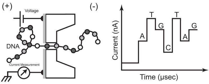
Although the resistive pulse mode has revealed a host of interesting features about DNA using both artificial and biological nanopores, nucleotide sequence is not one of them—at least not with unmodified nucleotides and linear DNA. Other DNA sense mechanisms have been proposed. Of particular interest is the so-called “tunneling” mode using transverse electrodes separated by the nanopore diameter [12] (Fig. 1). At dimensions commensurate with those of DNA, i.e. 2 nm, it is, however, questionable whether tunneling is the majority current contributor. The concept is based on the same tenants as Scanning Tunneling Microscopy (STM), which is known to have atomic resolution under ideal conditions. STM studies of DNA show promising results [13–15], and even suggest electron spectroscopy may be useful in distinguishing base pairs [16]. Computer simulations have also predicted the signal [17, 18] from a nanopore device employing tunneling mode current measurement through transverse electrodes. However, there is some debate about whether the geometric configuration of the base pair or its electronic properties will dominate [19], particularly when DC excitation is used for measurement.
Fig. 1.
Cross-sectional diagram of device (left) and anticipated output signal (right) for sequencing DNA
This paper presents a summary of the nanofabrication and initial testing of a high-speed DNA sequencing device based on a transverse electrode current measurement mechanism. A focused electron beam (FEB) milling technique capable of creating features on the order of 1 nm was used to create nanopores. Both DC and AC electrical characterization of the device were performed using gold nanoparticles as analyte. The results show promise for detecting and characterizing objects on the length scale of DNA. A low-noise, low-current, high-frequency amplifier for future, direct integration with the nanopore device was also fabricated and tested. It demonstrated noise and bandwidth performance sufficient for detecting the estimated signal from DNA.
2. Experimental
2.1 Device nanofabrication
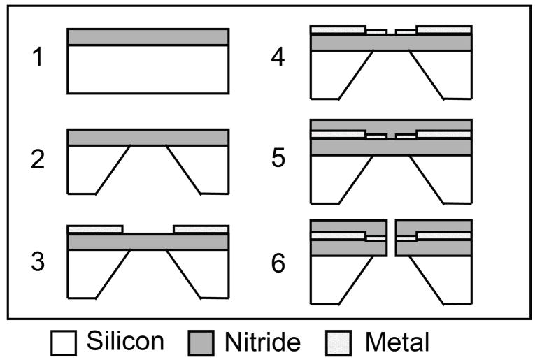
The device was fabricated on a thin (30–50 nm), stoichiometric, low-pressure chemical vapor deposited (LPCVD) silicon nitride membrane. A (100) silicon wafer substrate was used as the membrane supporting substrate and as a prelude for the future integration of current measuring electronics. The membrane, approximately 100 μm square, was formed by anisotropic etching of the silicon substrate (Fig. 2), using either crystallographic etching in KOH or deep reactive ion etching (DRIE). Bonding pads and metal interconnects were fabricated using standard photolithography, and thin chromium metal nanoelectrodes (10 nm thick, 2–50 nm separation) were fabricated using electron beam lithography and lift-off metallization. Devices were then coated with either 10 nm or 1 μm of PECVD silicon nitride. Devices with 1 μm of nitride had the silicon nitride immediately over the electrode gap and bond pads thinned to 10 nm by CF4/O2 reactive ion etching. All dielectric film thicknesses were measured optically using a spectroscopic ellipsometer and a nanospectrophotometer. A nanopore was formed between the two electrodes using an FEB milling technique (Fig. 3), exposing the electrodes at the edge of the nanopore.
Fig. 2.
Process flow for the creation of nanopore device. Silicon nitride deposition (1) is followed by an anisotropic silicon etch (or DRIE) (2). Optical lithography (3) and electron beam lithography (4) pattern metal layers, which are covered by more silicon nitride (5) and finally the nanopore is formed (6)
Fig. 3.
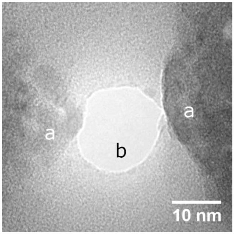
Plan view transmission electron micrograph of a typical nanopore device showing nanofabricated electrodes (a) and nanopore (b)
The electron beam milling technique was performed using a medium voltage (200–300 kV) field-emission transmission electron microscope (Philips CM200 or CM300). The nanopore formation process was studied using electron energy-loss spectroscopy (EELS) [20, 21]. After nanopore formation was complete, nanopores were analysed in-situ using bright and dark field stereomicroscopy for size and shape determination.
2.2 Device characterization
The nanodevice was tested electrically using gold nanoparticles as analyte. Gold nanoparticles were chosen because they are readily available in a wide range of sizes from 2–200 nm, have predictable electrical and material properties, and are relatively symmetrical. Gold nanoparticles suspended in aqueous solution and citrate stabilized with a net negative surface charge [22] were purchased from Ted Pella, Inc. The nanoparticle solutions also contained trace amounts of tannic acid and potassium carbonate.
Electrical testing of the nanodevice was carried out using both AC and DC excitation. The nanodevices were immersed in gold nanoparticle solution, a voltage was applied to one electrode and the current was monitored at the other electrode. An additional, isolated transmembrane voltage was applied in order to electrophorese the nanoparticles through the pore. Generally, the nanoparticle net negative surface charge from the citrate was sufficient for this purpose; however, in some cases either the pH of the solution was changed or trace amounts of mercaptoacetic acid were added to facilitate charge adsorption on the gold.
AC excitation was also used to characterize the nanopore device with and without nanoparticles. The current signal was measured using a commercially available current amplifier (LCA-200K-20M, FEMTO Messtechnik GmbH) connected to the chip through a needle probe. The current amplifier output was digitized and read using a custom, software-based lock-in amplifier platform. Both fixed frequency and swept frequency measurements were performed to determine admittance as a function of time and frequency.
2.3 Integrated current amplifier
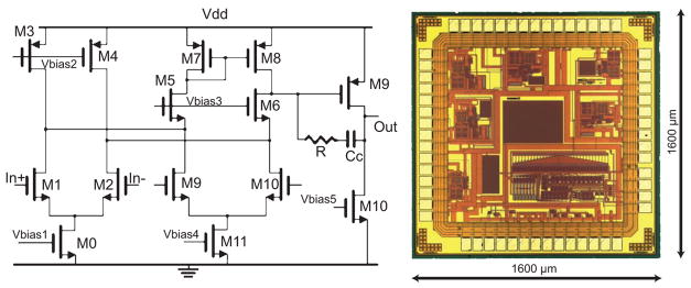
A low-noise, high-speed, low-current, transimpedance amplifier was designed and fabricated in an 0.35 μm CMOS process for future implementation of an integrated measurement system (Fig. 4) [23]. Six operational amplifiers, a 12-bit digital offset trimming circuit to remove up to 10 mV of input-referred offset, and an area for nanopore formation are included on the die layout. The silicon nitride membrane and nanopore fabrication can be performed post-IC manufacture, utilizing one of several, previously demonstrated methods [24–26]. The nanopore formation by FEB, which has no foreseeable IC incompatibilities, would be performed on individual die after separation from the wafer. Although FEB is not a batch fabrication procedure, it has the advantage of in-situ imaging and control of pore placement and geometry.
Fig. 4.
Circuit diagram (left) and die photograph (right) of custom low-current high-speed operational amplifier. Six amplifiers are shown on the periphery of the chip with a 12-bit digital offset corrector in the lower-right corner. The center portion is available for integration with a nanopore array
3. Results and discussion
3.1 Nanopore formation
The nanopore formation technique borrows from a well-known problem encountered in high-resolution imaging of sensitive samples with transmission electron microscopy. During imaging, it is commonly found that focused electron beams drill holes [27] or remove material from the sample. This problem was recruited into a precision nanofabrication technique to drill nanopores in specified locations ranging in diameter from less than 1 nm to 50 nm (Fig. 5) [28].
Fig. 5.
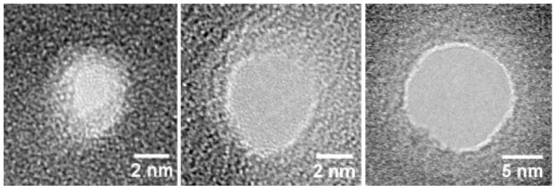
Plan view transmission electron micrographs of nanopores ranging in size from 1nm to 10nm
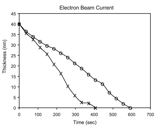
In-situ monitoring of the EELS plasmon loss peak during nanopore drilling was used to monitor progress (Fig. 6) and provide real time end point detection. The rate of material loss was roughly linear and proportional to the beam current density, suggesting knock-on displacement combined with back-surface sputtering as the dominant mechanisms, rather than a radiolysis process [20]. Nitrogen is removed roughly 50% faster than silicon leaving behind a silicon rich material. The sputtering of nitrogen atoms involves a binding energy of about 25eV and seems to be a necessary precursor to the sputtering of silicon.
Fig. 6.
Thickness of remaining silicon nitride as a function of time during nanopore formation for electron beam currents of 107 A/m2 (o) and 108 A/m2 (×). Thickness was determined by the intensity of the EELS plasmon loss peak
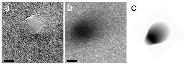
Examination of the completed holes using bright and dark field stereomicroscopy generally revealed a conical pore geometry with the apex at the electron beam entrance, although other geometries have also been observed (Fig. 7) depending on FEB conditions. Optimization of microscope parameters afforded excellent reproducibility (± 0.1nm) with pore diameters selectable from microscope dependent beam spot sizes. Pore formation does seem to be in competition with carbon contamination accumulation which provides a lower limit on the pore size of about 0.8 nm without special cleaning procedures.
Fig. 7.
Cross-sectional geometry determination of nanopore. Cross-sectional geometry is unclear by bright-field imaging alone (a) but comparison of dark-field mass-thickness contrast image (b) with simulated dark-field image (c) shows inverted cone shape is likely for this nanopore (all images taken with specimen tilted 20° relative to beam, scale bars 5 nm)
3.2 Device characterization
When devices were measured in the DC mode, sporadic current pulses were observed correlated to the presence of nanoparticles (Fig. 8). The experimental configuration did not permit a determination of whether the nanoparticle actually traversed the pore or just approached the electrodes sufficiently to perturb the electrode current. However, the current pulses were not present in the absence of the nanoparticles.
Fig. 8.
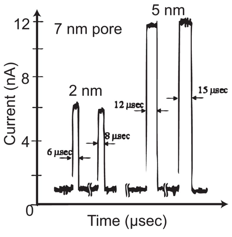
Current pulses observed using constant voltage source and gold nanoparticles (DC measurement mode)
In this experiment, a 7 nm diameter nanopore and 2 nm and 5 nm gold nanoparticles were used. A DC voltage of 1 Volt was applied through a 1 MΩ series resistor and the current was monitored as a function of time. A second, ground-isolated potential was applied across the membrane to electrophorese the nanoparticles through the nanopore. Although the nanoelectrode thickness is in principle many times the nucleotide-to-nucleotide spacing of DNA (0.34nm), the current is most likely to be emitted from the highest field region where the electrode to electrode spacing is the smallest. This phenomenon has long been understood in STM imaging and in field emission devices.
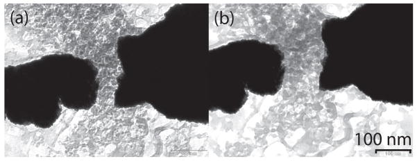
The magnitude and duration of the transient current pulses correlated with the nanoparticle sizes, however, the results were not reproducible. Changes in nanopore and electrode geometries were observed after repeated DC mode measurements, most likely due to a combination of surface-energy driven pore expansion or contraction and electrochemical electrode corrosion. Fig. 9 shows a TEM micrograph of a nanopore device after repeated electrical characterization in solution. Clearly, the electrodes have receded from the nanopore. More noble metals such as Pt and Au have also been employed as nanoelectrodes, however, the well-known surface motilities of the noble metals generally preclude their use. For example, shown in Fig. 10 is a set of TEM micrographs fabricated with Pt nanoelectrodes. Fig. 10(a) shows an electrode set upon first examination in the TEM and Fig. 10(b) shows the same electrode after only 5 minutes exposure to the TEM electron bombardment. The Pt has receded due to surface mobility and surface tension. The phenomenon is not restricted to electron bombardment, and the fine nanostructure is equally destroyed under modest, < 200 °C elevations in temperature.
Fig. 9.
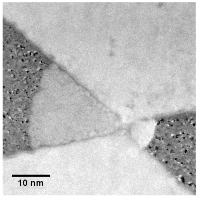
Plan view transmission electron micrograph of nanopore device after repeated measurements showing etched electrodes
Fig. 10.
Plan view transmission electron micrographs of Pt electrodes (a) initially and (b) after 5 min of electron beam exposure
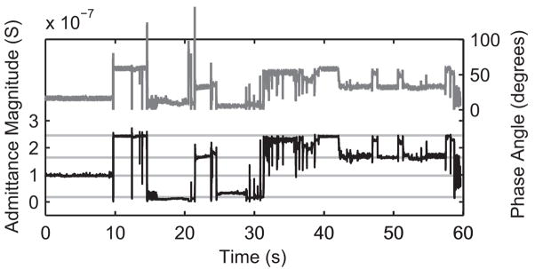
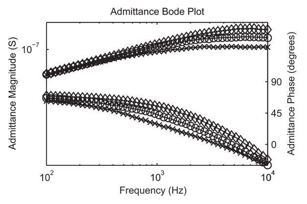
AC characterization of the nanodevices yielded variations in the admittance magnitude and phase over time. Fig. 11 shows the typical response of a 50 nm diameter nanopore in the presence of 20 nm gold nanoparticles. The time scale of the measurement precludes seeing individual nanoparticle transits, but does show a number of large phase and admittance shifts during measurements. These shifts were not observed when the same experiments were performed without nanoparticles in the solution. Upon closer investigation, the shifts are “quantized” at roughly regular admittance intervals. Based on previously reported studies of the dielectrophoretic attraction of gold nanoparticles [29–31], a model was developed that explains these shifts. During AC excitation of the nanoelectrodes, nanoparticles are attracted to the high field edge of the electrodes and form a weak association that effectively extends the nanoelectrodes, decreases the gap between electrodes, and increases the admittance (Fig. 12). The number and position of the “states” is a complicated function of the electrode gap and size of the nanoparticles, and more work is needed to understand them. The figure shows the best guess scenarios based on simple admittance calculations. Unless the nanoparticles become fused to the nanoelectrodes by applying a current pulse, the nanoparticles can be added or removed by changing the applied voltage or otherwise perturbing the system with fluid flow or mechanical vibrations. Dielectrophoretic capture of gold nanoparticles can be used to create designer nanoelectrode gap spacings [32]. Bode plots of the frequency response of the nanodevice taken in different “states” are shown in Fig. 13.
Fig. 11.
Variations in measured admittance magnitude (black line) and phase (dark grey line) during constant frequency AC excitation (20 nm gold nanoparticles in water). Light grey lines are a guide to the eye in observing quantized states. No variations were seen without nanoparticles present
Fig. 12.
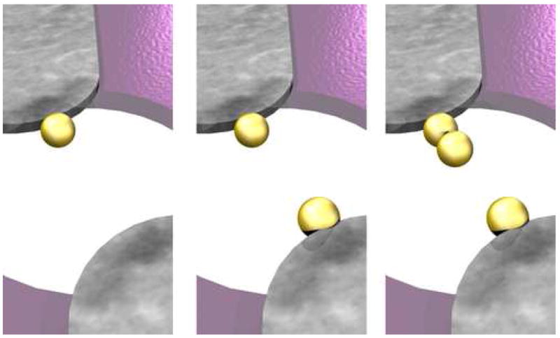
Depictions of several configurations of dielectrophoretically captured gold nanoparticles at nanoelectrode tips. Nanoparticles reduce effective gap width and increase measured AC admittance
Fig. 13.
Bode plots of variation in admittance with frequency for several different quantized states (10 nm gold nanoparticles in water)
3.3. Integrated current amplifier
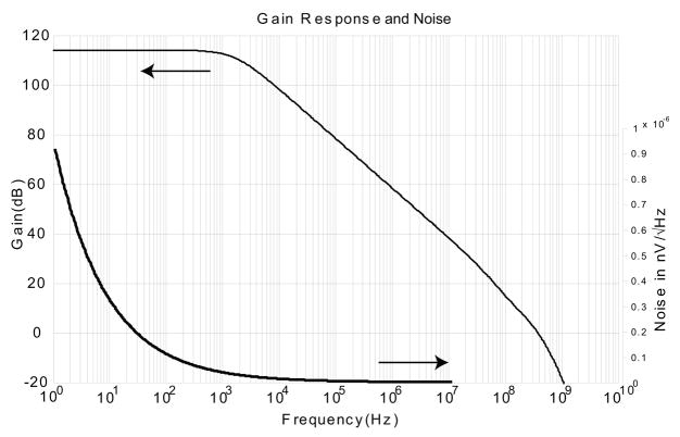
The custom current amplifier design achieved AC performance suitable for single nucleotide detection (Fig. 14). The unity-gain bandwidth of 300 MHz allows a closed-loop transimpedance of 10 kΩ to be used at 10 MHz. The power spectral density of the noise is expected to be less than 2nV/√Hz for frequencies greater than 1 MHz. A more complete explanation of design and performance is given in reference [23].
Fig. 14.
AC performance of custom integrated CMOS current amplifier. Unity-gain bandwidth is 300 MHz and noise power spectral density is less than 2 nV/√Hz at 10 MHz
4. Conclusion
A prototype nanopore device with integrated transverse nanoelectrodes for DNA sequencing has been fabricated and tested. Although DNA detection has not yet been verified, the device shows promise of realizing the sensitivity of STM and providing a platform for single nucleotide detection and sequencing of DNA. Both nanopore and nanoelectrode fabrication techniques may be extended to produce features at the 1 nm scale.
Electrical characterization of these devices indicates they can resolve signals generated by gold nanoparticles at the same dimensional scale as ssDNA. A low-noise, low current, high-frequency amplifier has been fabricated for direct integration with the nanopore device. The entire system is capable of integration into array form for massively parallel sequencing of DNA.
Acknowledgments
This study was supported by grants from the National Institutes of Health (NIH/NHGRI Grant 5 R01 R01HG03565), the David and Lucille Packard Foundation (Interdisciplinary Science Grant 2002-22776A), and the National Science Foundation (Grant 9986530). Fabrication and characterization were supported by the National Center for Electron Microscopy, Lawrence Berkeley Lab (U.S. Department of Energy, Contract # DE-AC02-05CH11231) and the Stanford Nanofabrication Facility (National Science Foundation NNIN, Grant ECS-9731293). We thank National Semiconductor for fabrication of the current amplifier.
Footnotes
Publisher's Disclaimer: This is a PDF file of an unedited manuscript that has been accepted for publication. As a service to our customers we are providing this early version of the manuscript. The manuscript will undergo copyediting, typesetting, and review of the resulting proof before it is published in its final citable form. Please note that during the production process errors may be discovered which could affect the content, and all legal disclaimers that apply to the journal pertain.
References
- 1.Kasianowicz JJ, Brandin E, Branton D, Deamer DW. Characterization of individual polynucleotide molecules using a membrane channel. Proc Natl Acad Sci USA. 1996;93:13770–13773. doi: 10.1073/pnas.93.24.13770. [DOI] [PMC free article] [PubMed] [Google Scholar]
- 2.Bayley H, Martin CR. Resistive-pulse sensing - From microbes to molecules. Chem Rev. 2000;100:2575–2594. doi: 10.1021/cr980099g. [DOI] [PubMed] [Google Scholar]
- 3.Dekker C. Solid-state nanopores. Nat Nanotechnol. 2007;2:209–215. doi: 10.1038/nnano.2007.27. [DOI] [PubMed] [Google Scholar]
- 4.Akeson M, Branton D, Kasianowicz JJ, Brandin E, Deamer DW. Microsecond time-scale discrimination among polycytidylic acid, polyadenylic acid, and polyuridylic acid as homopolymers or as segments within single RNA molecules. Biophys J. 1999;77:3227–3233. doi: 10.1016/S0006-3495(99)77153-5. [DOI] [PMC free article] [PubMed] [Google Scholar]
- 5.Bezrukov SM, Vodyanoy I, Brutyan RA, Kasianowicz JJ. Dynamics and free energy of polymers partitioning into a nanoscale pore. Macromolecules. 1996;29:8517–8522. [Google Scholar]
- 6.Fologea D, Uplinger J, Thomas B, McNabb DS, Li JL. Slowing DNA translocation in a solid-state nanopore. Nano Lett. 2005;5:1734–1737. doi: 10.1021/nl051063o. [DOI] [PMC free article] [PubMed] [Google Scholar]
- 7.Ju JY, Kim DH, Bi LR, Meng QL, Bai XP, Li ZM, Li XX, Marma MS, Shi S, Wu J, Edwards JR, Romu A, Turro NJ. Four-color DNA sequencing by synthesis using cleavable fluorescent nucleotide reversible terminators. Proc Natl Acad Sci USA. 2006;103:19635–19640. doi: 10.1073/pnas.0609513103. [DOI] [PMC free article] [PubMed] [Google Scholar]
- 8.Nakane JJ, Akeson M, Marziali A. Nanopore sensors for nucleic acid analysis. J Phys Condens Matter. 2003;15:R1365–R1393. [Google Scholar]
- 9.Li J, Stein D, McMullan C, Branton D, Aziz MJ, Golovchenko JA. Ion-beam sculpting at nanometre length scales. Nature. 2001;412:166–169. doi: 10.1038/35084037. [DOI] [PubMed] [Google Scholar]
- 10.Storm AJ, Chen JH, Ling XS, Zandbergen HW, Dekker C. Fabrication of solid-state nanopores with single-nanometre precision. Nat Mater. 2003;2:537–540. doi: 10.1038/nmat941. [DOI] [PubMed] [Google Scholar]
- 11.Kim MJ, McNally B, Murata K, Meller A. Characteristics of solid-state nanometre pores fabricated using a transmission electron microscope. Nanotechnology. 2007;18:205302. [Google Scholar]
- 12.Gierhart BC, Howitt DG, Chen SJ, Zhu Z, Kotecki DE, Smith RL, Collins SD. Nanopore with Transverse Nanoelectrodes for Electrical Characterization and Sequencing of DNA. Tech. Digest, 14th Int. Conf. on Solid-State Sensors, Actuators, and Microsystems, TRANSDUCERS ‘07; Lyon, France. June 10–14, 2007; [DOI] [PMC free article] [PubMed] [Google Scholar]
- 13.Tanaka H, Kawai T. Visualization of detailed structures within DNA. Surf Sci. 2003;539:L531–L536. [Google Scholar]
- 14.Driscoll RJ, Youngquist MG, Baldeschwieler JD. Atomic-scale imaging of DNA using scanning tunnelling microscopy. Nature. 1990;346:294–296. doi: 10.1038/346294a0. [DOI] [PubMed] [Google Scholar]
- 15.Yoshida Y, Nojima Y, Tanaka H, Kawai T. Scanning tunneling spectroscopy of single-strand deoxyribonucleic acid for sequencing. J Vac Sci Technol, B. 2007;25:242–246. [Google Scholar]
- 16.Hansma PK, Coleman RV. Spectroscopy of Biological Compounds with Inelastic Electron Tunneling. Science. 1974;184:1369–1371. doi: 10.1126/science.184.4144.1369. [DOI] [PubMed] [Google Scholar]
- 17.Lagerqvist J, Zwolak M, Di Ventra M. Fast DNA sequencing via transverse electronic transport. Nano Lett. 2006;6:779–782. doi: 10.1021/nl0601076. [DOI] [PMC free article] [PubMed] [Google Scholar]
- 18.Zikic R, Krstic PS, Zhang XG, Fuentes-Cabrera M, Wells J, Zhao XC. Characterization of the tunneling conductance across DNA bases. Phys Rev E Stat Nonlin Soft Matter Phys. 2006;74 doi: 10.1103/PhysRevE.74.011919. [DOI] [PubMed] [Google Scholar]
- 19.Zhang XG, Krstic PS, Zikic R, Wells JC, Fuentes-Cabrera M. First-principles transversal DNA conductance deconstructed. Biophys J. 2006;91:L4–L6. doi: 10.1529/biophysj.106.085548. [DOI] [PMC free article] [PubMed] [Google Scholar]
- 20.Chen SJ, Howitt DG, Gierhart BC, Smith RL, Collins SD. Electron Beam Drilling of Nanopores on Silicon Nitride Membranes Using a Transmission Electron Microscope. Microsc Microanal. 2007;13:534–535. [Google Scholar]
- 21.Chen SJ, Howitt DG, Gierhart BC, Smith RL, Collins SD. Electron Beam Hole-Drilling of Silicon Nitride Thin Films. J Appl Phys. 2007 in press. [Google Scholar]
- 22.Brewer SH, Glomm WR, Johnson MC, Knag MK, Franzen S. Probing BSA Binding to Citrate-Coated Gold Nanoparticles and Surfaces. Langmuir. 2005;21:9303–9307. doi: 10.1021/la050588t. [DOI] [PubMed] [Google Scholar]
- 23.Zhu Z, Tumati R, Collins S, Smith R, Kotecki DE. A low-noise, low-offset operational amplifier in 0.35 um technology. Tech. Digest, 13th IEEE Int. Conf. on Electronics, Circuits, and Systems (ICECS); Nice, France. Dec. 10–13, 2006. [Google Scholar]
- 24.Kurzawski P, Salo T, Baltes H, Hierlemann A. Towards a versatile DRIE: silicon pit structures combined with electrochemical etch stop. J Microelectromech Syst. 2006;15:840–848. [Google Scholar]
- 25.Rufer L, Domingues CC, Mir S, Petrini V, Jeannot JC, Delobelle P. A CMOS Compatible Ultrasonic Transducer Fabricated With Deep Reactive Ion Etching. J Microelectromech Syst. 2006;15:1766–1776. [Google Scholar]
- 26.Muller T, Brandl M, Brand O, Baltes H. An industrial CMOS process family adapted for the fabrication of smart silicon sensors. Sens Actuators, A. 2000;84:126–133. [Google Scholar]
- 27.Medlin DL, Howitt DG. Radiation-Damage Processes Affecting Electron-Beam Lithography of Inorganic Materials. Scanning. 1992;14:86–90. [Google Scholar]
- 28.Collins SD, Smith RL, Seldin MF. MicroInstrument for Rapid DNA Sequencing Via Nanopores, National Science Foundation Award #9986530. 1999 [Google Scholar]
- 29.Gierhart BC, Howitt DG, Chen SJ, Smith RL, Collins SD. Gold Nanoparticle Super Assembly by Dielectrophoresis. Tech. Digest, National Science and Technology Institute Nanotech 2007; Santa Clara, CA. May 20–24, 2007. [Google Scholar]
- 30.Gierhart BC, Howitt DG, Chen SJ, Smith RL, Collins SD. Frequency Dependence of Gold Nanoparticle Superassembly by Dielectrophoresis. Langmuir. 2007 doi: 10.1021/la701472y. [DOI] [PubMed] [Google Scholar]
- 31.Hermanson KD, Lumsdon SO, Williams JP, Kaler EW, Velev OD. Dielectrophoretic assembly of electrically functional microwires from nanoparticle suspensions. Science. 2001;294:1082–1086. doi: 10.1126/science.1063821. [DOI] [PubMed] [Google Scholar]
- 32.Khondaker SI, Yao Z. Fabrication of nanometer-spaced electrodes using gold nanoparticles. Appl Phys Lett. 2002;81:4613–4615. [Google Scholar]


