Abstract

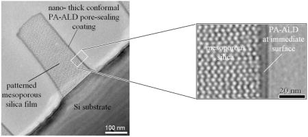
On a porous substrate, regular atomic layer deposition (ALD) not only takes place on top of the substrate but also penetrates into the internal porosity. Here we report a plasma-assisted process in which the ALD precursors are chosen to be non-reactive unless triggered by plasma, so that ALD can be spatially defined by the supply of plasma irradiation. Since plasma cannot penetrate within the internal porosity, ALD has been successfully confined to the immediate surface. This not only gives a possible solution for sealing of porous low dielectric constant films with a conformal layer of nm-scale thickness, but also enables us to progressively reduce the pore size of mesoporous materials in a sub-Å/cycle fashion for membrane formation.
As device dimensions in semiconductor integrated circuits (ICs) continue to shrink, low dielectric constant (low-k) materials are needed as interlevel dielectrics (ILD) to mitigate issues caused by reduced line widths and line-to-line spacings such as increasing RC-delay. To satisfy the technical requirements established by the microelectronics roadmap (where k values < 2 are ultimately specified), future generation ILD materials must incorporate porosity. However, the pores, typically on the order of angstroms to a few nanometers and interconnected at elevated porosities, can trap moisture, gas precursors and other contaminants in subsequent processing steps, making practical pore-sealing techniques essential to low-k implementation. [1–3]
To be useful for microelectronics applications, a pore-sealing coating must be conformal to the 3D topology of patterned ILD films. In addition, at the 65 nm or smaller technology node, it must be only several nm thick, so its impact on the overall ILD k value is negligible.[1] These requirements exclude most thin film deposition techniques with the exception of atomic layer deposition (ALD), for which the coatings are inherently conformal and precisely controlled at sub-nm thicknesses. However, on a porous substrate, regular ALD not only takes place on top of the substrate, but also penetrates into the internal porosity (see Supplemental Fig. 1), filling pores and drastically increasing the effective ILD k value.[4–6] Therefore, an approach capable of localizing ALD to the ILD surface and allowing spanning of the pores is needed.
Generally this is hard to achieve because ALD is a surface adsorption-based deposition process that takes place wherever gas precursor adsorption occurs, including throughout the complete network of connected internal porosity. Short precursor exposure times may reduce the ALD penetration depth, but with small ILD feature dimensions, even a 10 nm penetration depth means that a substantial portion of the ILD porosity would be filled.
Here we report a plasma-assisted process in which ALD is confined to the immediate surface, allowing pore sealing at minimal ILD thickness. To date, several groups have demonstrated the use of plasmas to enhance the extent of ALD reactions and achieve better film quality.[7–9] In our work, the purpose of the plasma is to define the location of ALD. If ALD precursors are chosen to be non-reactive unless ‘triggered’ by plasma, then, ALD can be spatially defined by the supply of plasma irradiation. In this regard it is important to recognize that the Debye length (μm) and the molecule mean free path in a typical plasma (μm-mm) greatly exceed the pore dimension of a porous low-k material (nm), thus plasma cannot penetrate (and ALD cannot occur) within the internal porosity.
The experiments were carried out in a self-designed, home-built plasma-assisted ALD (PA-ALD) system. The deposition chamber was a 25mm diameter Pyrex tube, evacuated by a turbomolecular pump to a base vacuum of 5×10⁻⁷ Torr. An RF coil surrounded the Pyrex tube for plasma generation. Samples were mounted in a remote plasma zone for reduced ion bombardment and plasma-heating effects (see Supplementary information). Oxygen and TEOS (tetraethylorthosilicate Si(OCH2CH3)4) were used as the precursors for SiO2. In the absence of plasma, they remain unreactive at room temperature. These precursors were admitted into the reactor alternately via pneumatic timing valves. A constant Ar flow of 15 sccm was used as the carrier gas as well as the purging gas.
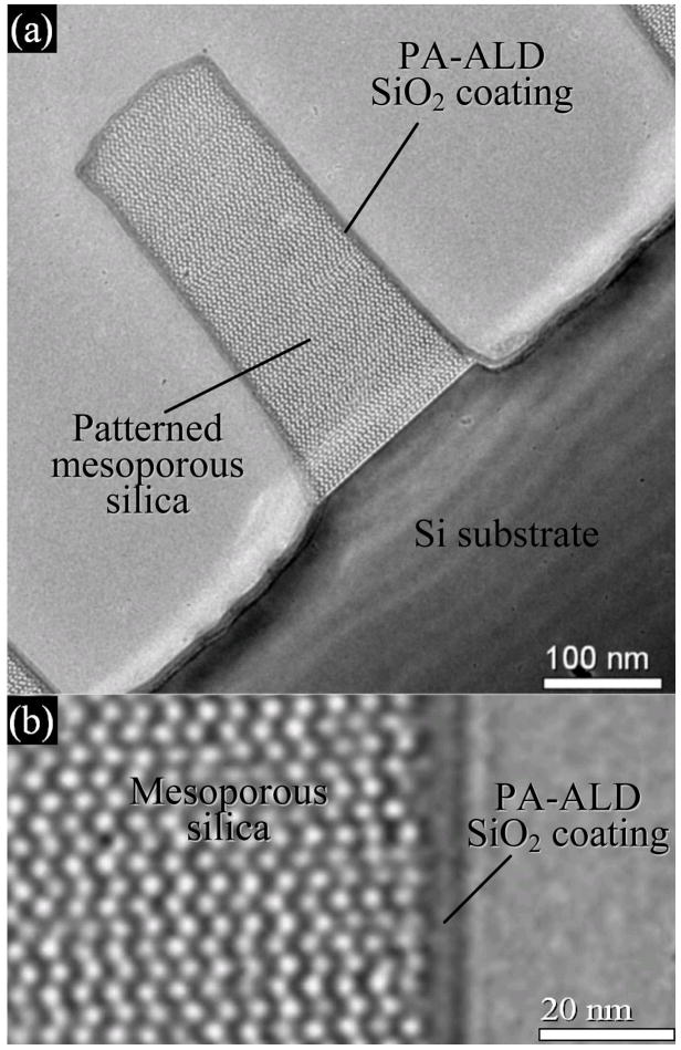
The mesoporous silica thin film samples were prepared on silicon substrates by evaporation-induced self-assembly.[10] The non-ionic surfactant Brij-56 was used to direct the formation of a cubic mesostructure characterized by a continuous 3D network of connected pores with diameters ~2-nm (Fig. 1b). These films exhibit excellent mechanical strength and thermal stability, along with an isotropic k and low surface roughness, important for etching or chemical mechanical polishing. With ~50 volume % porosity, the k value was measured to be 2.42 (Supplementary information) consistent with effective medium predictions. Prior to PA-ALD, the samples were patterned by interferometric lithography and etched with a CHF3/Ar plasma to create 400 × 400-nm trenches (Fig. 1a). Then the photoresist and any residual organics were removed by oxygen-plasma treatment.
Figure 1.
Cross-sectional TEM images showing: a) conformal 5nm thick pore-sealing coating of SiO2 prepared on a patterned mesoporous low-k silica film by plasma-assisted ALD; b) enlarged image at the interface between PA-ALD layer and the mesoporous film
Plasma-assisted ALD was performed by first introducing TEOS vapor into the reactor, followed by Ar purging to obtain a monolayer (or sub-monolayer) of adsorbed precursor. RF power was then delivered to the coil, creating an O2 and Ar plasma. The associated radicals convert surface-adsorbed TEOS into reactive silanols and may promote further conversion to siloxane. Following this, the deposition chamber was purged again to remove the residual gaseous products, completing one cycle. 150 cycles were performed, each cycle requiring 5 seconds.
Figure 1a and b show cross-sectional TEM images of the sample. A 5 nm thick SiO2 coating is observed as the smooth dark rim bordering the patterned mesoporous silica feature. Clearly, the coating is conformal to the patterned morphology and uniform in thickness. No penetration of the SiO2 into the porous matrix can be observed. The measured k of the corresponding planar sample equaled 2.49 (Supplementary information) consistent with minimal penetration of the PA-ALD layer.
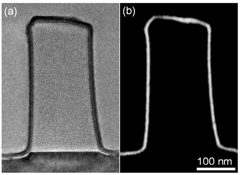
To verify the pore-sealing effectiveness, the PA-ALD coated sample was introduced into a conventional ALD reactor, where we performed thermal TiO2 ALD, shown previously to infiltrate surfactant-templated mesoporous silica. At 180 °C, the PA-ALD coated sample was treated with 100 thermal ALD cycles using TiCl4 and H2O as the precursors. Figure 2a is a regular cross-sectional TEM image, where we observe two ALD layers. The inner, lighter layer is the PA-ALD SiO2 coating, and the outer, darker layer is the TiO2 thermal ALD coating. The mesoporous low-k silica appears completely unaffected, suggesting that TiCl4 and H2O cannot penetrate through the PA-ALD SiO2 coating to form TiO2 in the underlying porous silica matrix. This is further supported by the Ti- mapping image in Fig. 2b. The bright border in this image represents the location of Ti, and corresponds to the TiO2 overlayer shown in Fig. 2a. Comparing the Ti- mapping image (Fig 2b) to the original regular TEM image (Fig 2a), no detectable TiO2 can be found beyond the PA-ALD SiO2 coating. Therefore, the PA-ALD SiO2 coating, although only 5 nm thick, is sufficiently dense and defect-free to seal the pores and protect the porous low-k silica from exposure to gaseous chemicals.
Figure 2.

TEM images demonstrating the pore-sealing effectiveness by PA-ALD: a) regular cross-sectional TEM image showing the mesoporous sample treated by PA-ALD pore-sealing process and then exposed to TiO2 ALD conditions; b) Ti- mapping image in the same area acquired with electron-energy-loss image filtering mode
Concerning the mechanism of room temperature PA-ALD of SiO2, we first note that the deposition rate is quite low, 0.03-nm/cycle, compared to 0.07–0.08-nm/cycle measured by George et al. for conventional NH3 catalyzed SiO2 ALD.[11] Conventional ALD uses multiple water/TEOS cycles, where water exposures hydrolyze ethoxysilane bonds to form silanols, and alkoxide exposure results in condensation reactions to form siloxane bonds. As for the related solution-based ‘sol-gel’ reactions, hydrolysis and condensation are bimolecular nucleophilic substitution reactions catalyzed by acid or base.[12] In PA-ALD, plasma exposure takes the place of hydrolysis, activating the alkoxide surface toward TEOS adsorption. Based on studies of plasma-enhanced CVD of SiO2 from TEOS and O2 performed by Aydil et al. [13] where silanol groups were identified after exposure of TEOS to an oxygen plasma, we expect silanols to form similarly during PA-ALD. However due to the monolayer (or sub-monolayer) ≡Si-OH coverage, we cannot quantify the extent of surface hydrolysis. Additionally we expect the plasma could serve a catalytic role by generating nucleophilic oxo radicals, ≡Si-O• that promote siloxane bond formation. Apparently at room temperature the extent of these plasma assisted hydrolysis and condensation reactions are less than for ammonia catalyzed hydrolysis and condensation reactions during conventional room temperature ALD [11], explaining the low deposition rates. Consistent with a low rate of siloxane bond formation is the highly conformal and dense PA-ALD layer indicative of a reaction-limited monomer-cluster growth process– in our case confined exclusively to the plasma-activated surface. [12]
Here we emphasize PA-ALD as a means of sealing pores. However with the very high degree of thickness control that we demonstrate (0.03-nm/cycle), which remains linear for atleast 150 cycles, we envision that, prior to complete pore sealing, we will progressively reduce the pore size of the mesoporous silica in a sub-Å/cycle fashion. This combined with the thin PA-ALD layer thickness could have very important implications for membrane formation, where extremely thin inorganic films with precisely controlled pore size could enable the synthesis of robust mimics of natural ion or water channels of interest for sensors and water purification.
Supplementary Material
Acknowledgments
This work was supported by the Army Research Office grant DAAD19-03-1-0227, DOE Basic Energy Sciences, Air Force Office of Scientific Research grant FA9550-04-1-0087, the NIH Nanomedicine Center program, and the SNL LDRD program. Sandia is a multiprogram laboratory operated by Sandia Corporation, a Lockheed Martin Company, for the United States Department of Energy’s National Nuclear Security Administration under Contract DE-AC04-94AL85000. We would also like to thank Prof. S. Brueck at UNM-Center for HTM for access to interferometric lithography.
References
- 1.2004 International Technology Roadmap for Semiconductors, Interconnect, SIA
- 2.Peters L. Semiconductor International. 2005 October;:49–53. [Google Scholar]
- 3.de Rouffignac P, Li ZW, Gordon RG. Electrochemical and Solid State Letters. 2004;7:G306–G308. [Google Scholar]
- 4.Cameron MA, Gartland IP, Smith JA, Diaz SF, George SM. Langmuir. 2000;16:7435–7444. [Google Scholar]
- 5.Ek S, Iiskola EI, Niinistö L. Langmuir. 2003;19:3461–3471. [Google Scholar]
- 6.Travaly Y, Schuhmacher J, Baklanov MR, Giangrandi S, Richard O, Brijs B, Van Hove M, Maex K, Abell T, Somers KRF. J Appl Phys. 2005;98:083515. [Google Scholar]
- 7.Elers KE, Winkler J, Weeks K, Marcus S. J Electrochem Soc. 2005;152(8):G589–G593. [Google Scholar]
- 8.Kim DH, Kim YJ, Song YS, Lee BT, Kim JH, Suh S, Gordon R. J Electrochem Soc. 2003;150:C740–C744. [Google Scholar]
- 9.Kim H, Detavenier C, van der Straten O, Rossnagel SM, Kellock AJ, Park DG. J Appl Phys. 2005;98:014308. [Google Scholar]
- 10.Brinker CJ, Lu YF, Sellinger A, Fan HY. Adv Mater. 1999;11:579–585. [Google Scholar]
- 11.Ferguson JD, Smith ER, Weimer AW, George SM. J Electrochem Soc. 2004;151:G528–G535. [Google Scholar]
- 12.Brinker CJ, Scherer GW. Sol-Gel Science: The Physics and Chemistry of Sol-Gel Processing. Academic Press; San Diago: 1990. [Google Scholar]
- 13.Deshmukh S, Aydil E. J Vac Sci Technol A. 1995;13:2355–2367. [Google Scholar]
Associated Data
This section collects any data citations, data availability statements, or supplementary materials included in this article.


