Abstract
This paper reviews the design and fabrication of polydimethylsiloxane (PDMS)-based conducting composites and their applications in microfluidic chip fabrication. Owing to their good electrical conductivity and rubberlike elastic characteristics, these composites can be used variously in soft-touch electronic packaging, planar and three-dimensional electronic circuits, and in-chip electrodes. Several microfluidic components fabricated with PDMS-based composites have been introduced, including a microfluidic mixer, a microheater, a micropump, a microdroplet controller, as well as an all-in-one microfluidic chip.
INTRODUCTION
Microfluidic devices for analytical and bioanalytical chemistry, micro-total-analysis systems (μ-TAS), or laboratories-on-a-chip incorporate a miniaturized analysis system in microfabricated chips in order to handle small volumes of samples, accelerate the speed of analyses, increase the resolution of separations, improve the selectivity and sensitivity of detection, and realize the automation of procedures.1, 2, 3, 4 Indeed, in μ-TAS, an entire analytical procedure can be integrated by constructing various components, such as micromixers,5 microheaters,6 microvalves and pumps,7, 8 microsorters and separators,9, 10 and microsensors and detectors,11 to realize specific functions including sample pretreatment, labeling reaction, separation, downstream reaction, detection, and others. A single portable biochip, which can integrate all such functions, is applied to various biological or chemical functions, such as polymerase chain reaction (PCR),12 protein separation,13 single-cell analysis,14 immunoassay,15 and chemical synthesis.16
The earlier methods to design and fabricate microfluidic component devices employed a silicon or glass wafer with photolithography, a technology offering advantages in microelectronics and microelectromechanical systems; however, the disadvantage is that the above wafers are not easily integrated with electrodes and also are difficult to be bonded with transparently multilayered structures.17, 18, 19 A simpler and cheaper alternative to photolithography is so-called “soft lithography.” This technology fabricates patterns in microchips by a replica molding, which entails the casting of a liquid prepolymer of an elastomer against a master’s surface having a predetermined relief structure.20, 21, 22 After curing or solidifying, the pattern is transferred from the master to the elastomer. Prepolymers used for the microfluidics so far include polycarbonate,23 polyimides,24 polyurethane,25 polymethyl methacrylate,26 polystyrene,27 widespread polydimethylsiloxane (PDMS), and others.28 PDMS, compared with other materials, has advantageous properties including typically low surface interfacial free energy, which enables it to conform to the surface of a master; an elastic characteristic, which allows it to be easily removed; optical transparence, which improves transmission of UV and visible light; and chemical inertness and durability besides.20 In this paper, we review the characteristics of PDMS materials and PDMS-based conducting composites, the design and fabrication of conducting PDMS-based microdevices, as well as their applications.
DESIGN AND FABRICATION OF PDMS-BASED CONDUCTING COMPOSITES
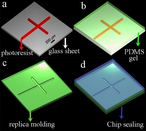
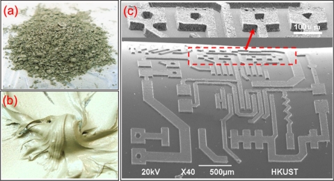
PDMS is a silicon-based organic polymer that has been widely used in the microfluidic chip fabrication owing to its good elastic property, nontoxicity, biocompatibility, optical transparence, noninflammability, chemical inertness, as well as conformability, among other attributes. Commonly, a chip is fabricated by soft lithography, which entails replica molding and chip sealing20, 21, 22 (Fig. 1). This method generates a variety of microstructures with the dimensions as small as ∼20 μm. Another important property of PDMS material is that it allows for fabrication of other microelectromechanical devices, such as microvalves, micropumps, micromixers, and microheaters.29 However, PDMS is an inert polymer, lacking conductive and magnetic properties. Besides, due to the weak adhesion between metal and PDMS, it is difficult, while fabricating microdevices, to pattern metallic structures on its surface or into the bulk. Hence, the integration of conducting structures into bulk PDMS has been a critical issue, especially as regards electrical devices, which require electrodes for the signal control and detection. Recently, some new synthesis processes have been developed to transform pure PDMS material to a conductive or a magnetic composite by the addition of carbon black powder or iron particles, respectively.30 Very recently, Niu et al. developed a method of patterning conductive structures using PDMS-based conducting composites, synthesized by uniformly mixing conductive micrometer silver or nanometer carbon particles with PDMS gel [Figs. 2a, 2b].31 The silver and carbon black particles were easy to mix with the PDMS gel owing to their desirable wetting characteristics. The conductivities of the two types of composites increased rapidly when the concentrations exceed threshold values of 83 and 10 wt %, respectively. In the experiment, the gel was embedded into a photoresist mold on a glass substrate to pattern the conductive composites; after baking, the gel was cured into a solid, and the designed part of the conducting composite was retained on the substrate by removing the photoresist (the fabrication process can be found in Ref. 31). Scanning electron microscopy images of electric circuit fabricated with conducting PDMS composites are shown in Fig. 2c. The dimensions of the patterns can range from tens to hundreds of micrometers. The experimental results indicated that two-dimensional (2D) and three-dimensional (3D) conducting microstructures were constructed and integrated into PDMS bulk material. The advantage of using PDMS-based conducting composites is the ease of bonding and embedding microstructures into PDMS-based microchips, forming electric signal connections in a 2D or 3D microstructure, thereby greatly enhancing the potential functionalities in microfluidic chips.
Figure 1.
Schematic illustration of the procedure for preparing a simple PDMS-based microfluidic chip. (a) Fabricate master by photolithogray using photoresist. (b) Cast PDMS prepolymer and cure. (c) Peel off PDMS replica with designed pattern. (d) Seal the replica with another flat PDMS.
Figure 2.
The silver submicron particles and their mixture with PDMS gel are shown in (a) and (b), respectively, while (c) illustrates the patterning of conductive circuit with PDMS-based conducting composite. An enlarged view of the dashed-line square is indicated by the arrow.
MICROFLUIDIC COMPONENTS
Fabrication of microfluidic chips from PDMS
Many research groups have made considerable effort to construct, by photolithographic technology, various microfluidic components on silicon, glass, and polymer substrates in μ-TAS including hydrodynamic (micropump and microvalve), thermodynamic (microheater), and electrodynamic (microelectrode) devices, as well as detection units (microsensors and microdetectors).20, 32 Recently, PDMS-based microfluidic devices have received much attention, and there has been considerable progress in fabricating PDMS-based microfluidic devices with multiple functionalities, the ultimate goal is the attainment of lab-on-a-chip integration.30, 33, 34 These efforts have benefited from the development of the soft lithography microfabrication method. In this context, PDMS has played an important role, not only served as the stamp for pattern transfer but also as a unique material in chip fabrication. These microfluidic devices fabricated with PDMS material include, but are not limited to, fundamental passive or active microvalves, micropumps, micromixers, microheaters, microsorters, separators, microsensors and detectors, etc.
Microfluidic valves
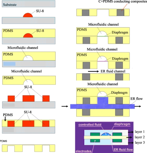
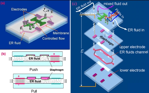
Microfluidic valves are one of the fundamental components of hydrodynamic devices, controlling the movement of fluids by means of flow regulation, on∕off switching, and sealing of liquids, gases, or vacuums.8 Usually, microvalves are controlled or actuated by piezoelectric elements,1 pneumatic solenoid,30 hydrogels,35 or other means. Their actuation principles are varied as reviewed by Oh and Ahn.8 For example, Frevert et al.36 reported a pneumatic microvalve chemotaxis device fabricated by soft lithography using PDMS materials to track migration of individual neutrophils. The device was a three-PDMS-layer stacked structure in which the top layer was a fluidic channel, the bottom layer was a dead-end pneumatic channel, and the middle layer was a 12-μm-thick moving PDMS membrane fabricated by spin coating and curing a thin layer of PDMS precursor solution onto a featureless silicon wafer. The microvalve was opened or closed by applying negative pressure (∼30 kPa) or positive pressure (∼10 kPa), respectively, to its pneumatic channels. Niu et al.37 introduced an electrodynamic and digitally addressable microvalve for millisecond-fast response time to control other fluid flows. The valve is actuated by smart giant electrorheological (GER) fluid,38 which is a type of colloidal suspension exhibiting solidlike behaviors, such as the transmission of shear stress under an applied field of 1–2 kV∕mm. The transformation from liquidlike to solidlike behavior is relatively quick, of the order of 1–10 ms, and reversible. Such a controllable variation in the rheological property makes a wide variety of potential applications possible, such as clutching, vibration damping, and valves. Figure 3 is a schematic design of PDMS-based multilayered GER microvalves fabricated by soft lithography. The electrode material is a composite synthesized by mixing PDMS and carbon black at a carbon concentration of 25% (w∕w) to form so-called C+PDMS gel. After being patterned and cured at 80 °C for 1 h, a 300-μm-thick C+PDMS hardened sheet was achieved (the black block in Fig. 3). The sheet (film) resistance of the C+PDMS electrode was measured at about 150 Ω∕cm by four-point probe measurement. In operation, the flexible diaphragm sandwiched between the ER channel and the flow channel is pull and push actuated by the on-off voltage applied to ER fluid. The pressure increases exponentially between the upstream and downstream valves as the electric field increases as a result of the viscosity variations in ER fluid under different field strengths.
Figure 3.
Flow chart of the fabrication of GER microvalve with embedded C+PDMS electrodes and its working principle. When ER fluid flows inside layer 2, the pull and push action of the diaphragm is realized by applying a voltage across the electrodes.
Microfluidic pump
Microfluidic pumps are another fundamental component in a microfluidic system used to displace fluid inside chips. Many types of pumps have been designed and fabricated for different mechanisms, for example, the piezoelectric transducer actuator pump utilizing electrical∕mechanical energy conversion.39 Wang and Lee40 fabricated a PDMS-based pneumatically driven peristaltic micropump. The maximum pumping rate demonstrate by this micropump was 7.43 μl min−1 provided by a micropump with seven membranes actuated by 20 psi air pressure and 9 Hz operation frequency. Atencia and Beebe41 introduced a novel magnetically driven biometric micropumping system. The pump, using vortices shed by an oscillating ferromagnetic bar inspired by the behavior of swimming animals and flying insects, has a range of operation from 3 to 600 μl min−1. Wang et al.42 reported a high-pressure electro-osmosis micropump fabricated by bonding a silica monolithic matrix within a 100-μm-inner-diameter fused silica capillary. The maximum flow rate and pressure generated by this pump were 2.9 μl min−1 and 3 atm for de-ionized water at 6 kV applied voltage, respectively. Elsewhere, there are still other designs based on various pumping mechanisms including pneumatic pumps, electrostatic pumps, shape memory alloy pumps, and more. However all these pumps can be categorized into two classes: (1) displacement (mechanical) pumps incorporating moving parts such as check valves and diaphragms or (2) dynamic pumps. Almost all the displacement pumps are closely related; that is, they incorporate, to a greater or lesser extent, the principles of valves discussed above.7, 43
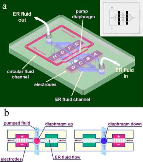
The design and fabrication of PDMS-based pumps in recent years have paralleled the development of soft lithography technology, which provides for better integration of microfluidic devices. For example, Weibel et al. fabricated a screw-valve-actuated PDMS-based pump that offers the advantages not only of storing multiple reagents in chips but also of controlling the rates of reagent flow.44 Liu et al.45 designed and fabricated a GER fluid-driven pump actuated by electric signals and applied to eight PDMS-based conducting electrodes [shown, respectively, from A to H in Fig. 4a]. In this design, a five-layer structure was embedded inside the PDMS chip, the bottom layer channeling ER fluid that can affect the flow of the circulating fluid on the top layer via the pull-push movement of the diaphragms between two pairs of electrodes. That is, when the voltage is applied to one pair of electrodes, the viscosity of the ER fluid between them increases, thereby slowing or even stopping the flow velocity of ER fluid. This causes the pressure to accumulate or decay under the diaphragm between two pairs of electrodes, thereby pushing or pulling the diaphragm upward or downward, respectively [Fig. 4b]. The pumped flux varies as a function of the intensity and frequency of the electric field, respectively. For example, if the intensity of all of the signals is fixed at 2 kV∕mm, the flux reaches a peak at about 1.3 μl s−1 at a frequency of ∼35 Hz, whereas if the frequency is fixed at 10 Hz and the applied electric field is varied, the flux increases monotonically with the field in an exponential dependence from 0 to 0.8 μl s−1 when the field is between 0.4 and 2.4 kV∕mm−1. The direction of the fluid flow and the pumped flux can also be controlled through digitized programmable eight-electrode action sequences.
Figure 4.
(a) Schematic illustration of the micropump, with its 3D structure, inside the microfluidic chip. The chip actuated by ER fluid controls the fluid circulation in the upper layer. The right upper inset is a picture of the fabricated device. The ER fluid channel is 500 μm wide and deep, the circular fluid channel is 0.6 mm wide and 1 mm deep. (b) The principle of ER valve’s operation is illustrated schematically by showing the deformation of a single diaphragm via pumped ER fluid (Ref. 45).
Microfluidic mixer
Rapid mixing of two or more streams of fluids is an important issue with regard to various microfluidic devices. Typically, there are two mixing modes, the passive mode and the active mode.5 The former depends only on diffusion or chaotic advection, which induces 3D helical fluid motions from patterned structural asymmetries that can fold streams into highly nested thin slices so as to facilitate local molecular interdiffusion. For example, Stroock et al.46 reported a staggered herringbone passive mixer to reduce the mixing lengths that stretch and fold the volumes of fluid over the cross section of the channel.
Active mixers differ from the passive type in that the external energy is intentionally input into the system to help achieve chaotic mixing. These external energy sources include, but are not limited to, electrokinetics (e.g., Lee et al.47 reported an active electrokinetically driven mixer utilizing zeta potential variations based on electro-osmotic flow), surface acoustic wave (e.g., Liu et al.48 developed an acoustically driven mixer based on the acoustic microstreaming principle; Shilton et al.49 demonstrated increased efficiency in particle concentration∕separation and in generating intense micromixing in microliter drops by using concentric circular and elliptical transducers to focus the wave), and magnetohydrodynamics (Ryu et al.50 fabricated a magnetic stir bar composed of a free rotating rotor to which was applied a rotating external magnetic field).
A cross-stream active mixer represents a system in which the flow in the main microfluidic channel is perturbed by actively controlled side-channel flows.51, 52 Niu et al.53 integrated an active chaotic mixer with a PDMS-based chip to be actuated by GER fluid valves. The mixer consists of a main flow channel and six pairs of orthogonal side channels. The operation of the mixer chip relies on the perturbation of the main channel x-direction flow by cross-stream side-channel y-direction flows. The side-channel flows are driven by pressure changes in the ER fluid channel and move through thin membranes at the bottom of the control bars located at the end of each side channel (Fig. 5). Figure 5b shows schematically the working principle of the ER valves. During operation, square-wave electrical voltage signals (0–800 V) are applied between the PDMS-based conducting electrodes connected to a high-pressure source on one side and a low-pressure source on the other in order to close or open the ER fluid flows so that the membranes on the two sides of the main channel can be pushed and pulled alternately, leading to pulsating sinusoidal cross-stream flows in the six pairs of side channels. The GER effect assures that the ER control channel can modulate large shear stress, thereby supplying large perturbations; such modulations can drive the membrane area by as fast as 20 Hz or above due to the fast (milliseconds) response of the ER fluid and the rapid pressure buildup used in the design.
Figure 5.
(a) Schematic picture showing the PDMS active mixer design and construction. The overall chip size is 3×1.5 cm2. (b) Schematic illustration showing the working principle for the push and pull ER valve for one cross-sectional area of the ER fluid channel and control bars. (c) Four-layer structure of the integral micromixer (Ref. 37).
Microfluidic heater
The microfluidic heater is a ubiquitous element in the μ-TAS, enabling multiple functions such as those involving physical and chemical sensors, chemical reactors, pumps, and other devices. A common design of these microheaters is thin metallic or doped-Si layers on a dielectric (or insulating) substrate, which is often a freestanding membrane to reduce the thermal mass of the system. For example, Arata et al.54 patterned nickel on a glass plate with sputtering and photolithography in fabricating a thin-film microheater. The heater heats its internal and external area in 1 ms by Joule heating generated by a thermal source.55
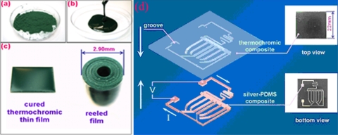
Thus far, there have been only a few reports on heaters fabricated with conducting PDMS composites, which probably reflect difficulties entailed in electrode fabrication and thermal field distribution in PDMS matrices as well as inertial thermal conductivity (about 0.15 W∕m K). However, doping conductive particles such as silver and carbon cannot only increase the electrical conductivity but also thermal conductivity. For example, Cong and Pan56 doped 17%–21% by volume silver powder in the PDMS matrix to obtain superb thermal conductive PDMS of 71–81 W∕m K, which is thought to be mainly attributed to the conductivity of silver filler. Liu et al.57 fabricated a flexible display device using PDMS∕silver-based composites as electrodes and formed of two composite materials: A thermochromic polymer sheet for the upper layer, produced by mixing thermochromic powder with PDMS [Figs. 6a, 6b, 6c], and a silver-embedded PDMS conductive composite electrode in a patterned logo for the lower layer [Fig. 6d], produced by the soft lithographic technique. Conducting composites offer the advantages of ease in patterning microconducting wires and in integrating electrical circuits. When voltage is applied to the two outstretched electrodes, the resulting electrical current will generate localized heating to the thermochromic layer that lies directly above the conducting wires. Once the local temperature rises to 60 °C or above, the color of the thermochromic layer promptly changes from dark green to white, leading to a visible, white image of the logo.
Figure 6.
(a) Thermochromic powder. (b) Liquidlike composite formed by mixing powder with PDMS gel. (c) Thin film of thermochromic composite. (d) Schematic illustrations of the display structure. The logo-patterned conductive wirings are shaped from silver microparticle-PDMS composite by using soft lithography. The conductive wire pattern is embedded into the thermochromic sheet. The insets show the top and bottom views of the fabricated device (Ref. 57).
Microfluidic thermal sensor
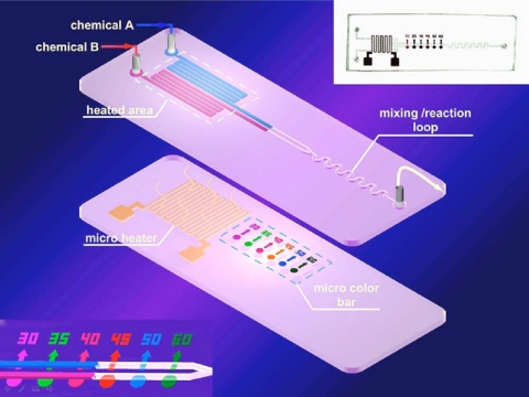
Recent interest in microfluidic chips for chemical and biological functions has also focused on thermal detection and control, as such functionalities are important in microreactions and bioprocesses, for instance, in experiments regarding DNA sequencing and cell biology applications.58 Platinum thin film has commonly been used as a temperature sensor in microchips.59 Thermal microscopic scanning, using fluorescent particles as sensors, has also been employed.60 In another approach, infrared cameras are frequently utilized to not only obtain surface temperature distributions via images61 but also constitute a feedback system for temperature control.62 Liu et al.63 reported the fabrication of a chemical reactor with PDMS-based thermochromic microcolor bars, which together function as a local temperature indicator inside the microfluidic chip, being sensed optically. The top layer was an ordinary PDMS chip with two elongated serpentine inlets to preheat the reactants. The upper layer was a PDMS∕silver-based microheater with thermochromic bars formed by mixing different thermochromic powders with PDMS gel and subsequently spun coated (Fig. 7). The color bars varied in color when heated from 30 °C to their transition temperature of 60 °C and above. Together with the embedded PDMS∕silver-based microheater and optical sensor, microfluidic chips can easily be monitored in their local thermal characteristics and controlled through a feedback electronic system.
Figure 7.
Diagrams of the optical-electrical temperature sensing and control processes. Combined with computer storage of calibrated control signals, this process can achieve accurate local temperature control in microfluidic devices. The process is operated via a control box shown in the upper right panel (Ref. 63).
MICROFLUIDIC DROPLET DETECTION AND MANIPULATION
Compared to conventional batch methods, μ-TAS has the ability to use very small quantities of sample to carry out fast separation and detection with high sensitivity and resolution. For example, it can shorten the time of DNA amplification and increase the PCR throughput, since the high surface-to-volume ratio within the microfluidic environment enables heat to be dissipated rapidly, thus reducing the thermal capacity of the PCR system and improving thermal cycling efficiency. The development of general on-chip detection methods, as reviewed by Schwarz et al.,11, 64, 65 has comprehended optical detection (especially laser-induced fluorescence), electrical detection (potential titration, capacity sorting, amperometric detection, and reactance measurement66), microwave-based detection, mass spectrometry, magnetic resonance detection, and other functionalities. Although optical detection methods are the most widely used10, 67 [e.g., employing either a photodiode for simple counting or a high-speed charge-coupled-device camera with image processing for detection of more detailed characteristics], large optical detection devices limit the advantages of portable chips. Nowadays, part of the driving force behind the future of μ-TAS is to exploit more direct and convenient electrical approaches to the signal collection considering the overall miniaturization and automation requirements.
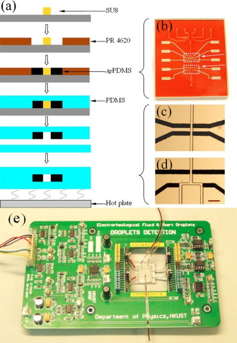
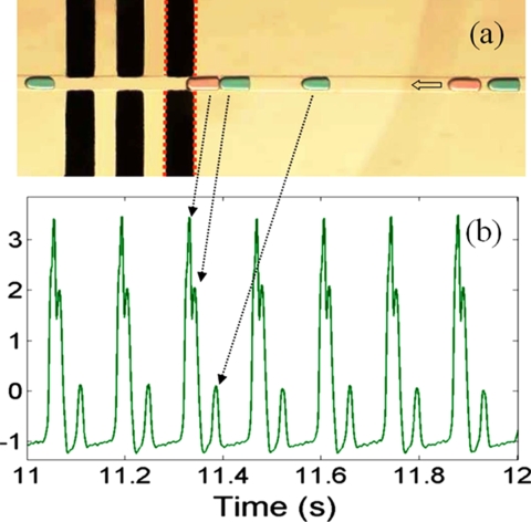
Sensing and detection involving electric fields, comparable to optical detection, has been put forward as an alternative.10 Electrical detectors meet the requirements of μ-TAS for in-field uses. Amperometric detection, for example, is suitable, owing to its low limits of detection, high selectivity, and compatibility with microfabrication techniques. Moriera et al.68 fabricated a multichannel PDMS∕glass-based analytical microsystem with patterned Ag electrodes for parallel amperometric detection. In the area of sensing and detecting noncontinuous volume in the forms of droplets,9, 67, 69, 70 as droplet size and distance can vary spatially and temporally, Niu et al.71 introduced a capacity detection method to detect droplet size, shape, and composition. They employed a multistage process and soft lithography to fabricate the microfluidic chip with embedded parallel electrodes [Figs. 8a, 8b, 8c, 8d]. The electrodes were made by mixing micron-sized Ag particles with PDMS gel. Electrical sensing or detection often requires the array and integration of multiple electrodes into chips. The common method is to pattern a thin layer of conductive materials on the surface of a wafer. However, it is not easy to fabricate two parallel electrodes on the opposite sides of a microchannel, as multilayer bonding is almost inevitable. By installing a pair of parallel electrodes across the microfluidic channel, very small capacitance variations can be detected when a droplet passes through. Due to the electrode’s design and feedback electronic circuit [Fig. 8e], real-time and accurate determination of the size, shape, and composition of droplets (having pico- to nanoliter volumes) is available. The operational frequency can reach up to 10 kHz, a speed that is difficult to realize by conventional optical means. Thus, capacitive measurement of droplets has the potential to be a simple, fast, and less expensive method that can be integrated into portable laboratory chips for in situ detection and control of droplets (see Fig. 9).
Figure 8.
(a) Flow chart of the microfluidic chip fabrication with parallel electrodes using soft lithography for droplet detection and control. (b) An optical image of the channel mold and conductive components. (c) and (d) are optical images of the droplet detection area and directional flow control area. The scale bar in (d) is 200 μm. (e) An optical image of the circuit board and the mounted chip for droplet detection (Ref. 71).
Figure 9.
(a) An optical image of a group of water droplets with different sizes. A small amount of dye was added for labeling. (b) The detected signals (Ref. 71).
INTEGRATED ALL-IN-ONE MICROFLUIDIC DEVICES
The concept of μ-TAS entails the integration of the different steps of an analytical process into a miniaturized flow system in order to realize fast, automated analysis of very small sample volumes.3, 72 These steps include functionalities such as sample prehandling, mixing and separation, sorting and detecting, transportation, recovery, and automation for reproducibility.73, 74 Microvalves, pumps, heaters, and mixers, among other devices usually provide the means for sample pretreatment, mixing, and transportation, whereas microsensors, detectors, sorters, separators, and others make their contributions in the sample post-treatment process. For example, Fu et al.69 developed an integrated microfabricated cell sorter using PDMS and soft lithography, which includes peristaltic pumps, dampers, switch valves, as well as input and output wells, to realize automated sorting and recovery of cells on the chip. A single microchip with integrated functions was reported for application to the purification of nucleic acids, a process which includes cell isolation, cell lysis, DNA and mRNA purification, and recovery, in sequence.75 Lee et al.33 fabricated an integrated chip for chemical synthesis of sensitive compounds. Dodge et al.76 realized the electrophoresis separation, selection, and digestion of a protein of interest in a single chip for mass spectrometry identification. Cheng et al.77 incorporated bioparticle filtering, focusing, sorting, trapping, and detecting into one chip in order to achieve multitarget pathogen detection.
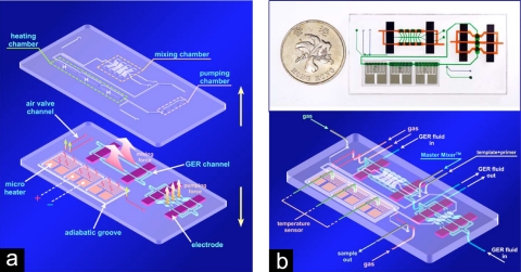
With a PDMS-based conducting electrode system, Liu et al.78 demonstrated a highly integrated microfluidic chip having the functionality of DNA amplification (Fig. 10). The integrated chip was fabricated by soft lithography using PDMS with embedded Ag∕carbon-PDMS electrodes, combining a GER-actuated micromixer and micropump with a microheater and temperature sensor. The chip was mainly composed of two layers where the lower layer was the control layer that dictates the status of the main reaction channel located in the upper layer. Elastic PDMS diaphragms sandwiched between the lower and upper layers serve to separate the fluids in the two layers, as well as to displace the reaction fluids in the upper layer channels via their up and down elastic deformations. The latter is the basic actuation mechanism of the GER fluid pump as described above. Two GER fluid channels (marked with blue) were used for activating the micromixer and micropump. There are three branch channels for the micropump, each sandwiched between a pair of PDMS-based electrodes. Under a series of coordinated electrical signals applied to the three electrodes (on the three branch channels), pressure differences will be established by GER pumping mechanism so that a pumping action is generated by the diaphragms to propel the fluids in the upper-level main channel (with flow direction perpendicular to the three branch channels). For the mixer, there are two GER fluid channels with two pairs of electrodes sharing a common ground. Pressure conditions in the two branches are designed to be opposite in phase and alternating in time, leading to a pulsating flow in mixer’s side channels (that are perpendicular to the main channel), via the actions of the diaphragms. The pulsating flow of the side channels is what drives the mixing action in the main channel. There are also three air valve channels distributed within the lower layer. Driven by compressed air, they produce on-off functions to control the flow of microreagents during the PCR process. There is a heater array comprising three adjacent microheaters. With electrical control signals, desired temperatures can be maintained within the helical patterned areas in the three heating chambers located at the upper layer. To avoid interferences among the three heaters, an adiabatic groove is made to surround each of the heaters for thermal insulation. With such a highly integrated device, this system demonstrates a flexible electrode array, digital control characteristics, and high PCR efficiency.
Figure 10.
(a) Two-layer structure of the integrated chip of which the topper layer contains the flow channels for PCR reagents and the lower layer flows GER fluid which constructs micropump and mixer. The patterned electrodes for the heater and temperature sensor are also located in this layer. (b) Full view of the chip. The upper panel shows an image of the fabricated device, placed beside a one dollar Hong Kong coin (Ref. 78).
CONCLUSIONS
Until now, PDMS-based conducting composites have been composed mainly of carbon black and silver particles on PDMS substrates. The composites inherit good electrical conductivity from the embedded particles as well as the elastomeric characteristic from PDMS, which render them suitable for the soft lithography process and feasible for integration with other devices. Composites of this type enabled a methodology for constructing planar and 3D microstructures via soft lithography. Different patterns of electrodes can also be fabricated by soft lithography using these materials. Hence various electrical microfluidic devices including micromixers, pumps, valves, heaters, and thermal sensors are achievable. GER fluids as smart materials are incorporated into electrodynamic devices such as mixers, pumps, and valves to realize controllable sample mixing and transportation. Such independent functional devices can be conveniently integrated to carry out multistep chemical or biological reactions, for example, PCR. However, PDMS-based conducting composites have some disadvantages, for example, a PDMS elastomer has a very low Young’s modulus compared to other metals and the cracks usually appear in the doped layer when it elongates and therefore causes an electrical failure. The conducting PDMS-based heater is not able to sustain high temperature due to the properties of PDMS. To improve the stability and reproducibility of conductivity, doped particles need to be modified to increase the compatibility between an inert PDMS matrix and fillers in the future. Nevertheless, the preliminary results obtained with PDMS-based conducting composites, especially the applications in microfluidic fabrication, are very promising and further intensive investigations should be carried out in the future.
ACKNOWLEDGMENTS
This work was supported by Hong Kong RGC research Grant No. HKUST 603608 and partially by the Nanoscience and Nanotechnology Program at HKUST.
References
- Reyes D. R., Iossifidis D., Auroux P. -A., and Manz A., Anal. Chem. 10.1021/ac0202435 74, 2623 (2002). [DOI] [PubMed] [Google Scholar]
- Ng J. M. K., Gitlin I., Stroock A. D., and Whitesides G. M., Electrophoresis 23, 3461 (2002). [DOI] [PubMed] [Google Scholar]
- Chen L., Manz A., and Day P. J. R., Lab Chip 7, 1713 (2007). [DOI] [PubMed] [Google Scholar]
- Whitesides G. M., Nature (London) 10.1038/nature05058 442, 368 (2006). [DOI] [PubMed] [Google Scholar]
- Nguyen N. -T. and Wu Z., J. Micromech. Microeng. 10.1088/0960-1317/15/2/R01 15, R1 (2005). [DOI] [Google Scholar]
- Yeom J., Field C. R., Bae B., Masel R. I., and Shannon M. A., J. Micromech. Microeng. 18, 12500 (2008). [Google Scholar]
- Woias P., Sens. Actuators B 10.1016/S0925-4005(04)00108-X 105, 28 (2005). [DOI] [Google Scholar]
- Oh K. W. and Ahn C. H., J. Micromech. Microeng. 10.1088/0960-1317/16/5/R01 16, R13 (2006). [DOI] [Google Scholar]
- Bruin G. J. M., Electrophoresis 21, 3931 (2000). [DOI] [PubMed] [Google Scholar]
- Pamme N., Lab Chip 12, 1644 (2007). [DOI] [PubMed] [Google Scholar]
- Schwarz M. A. and Hauser P. C., Lab Chip 10.1039/b103795c 1, 1 (2001). [DOI] [PubMed] [Google Scholar]
- Guttenberg Z., Müller H., Habermüller H., Geisbauer A., Pipper J., Felbel J., Kielpinski M., Scriba J., and Wixforth A., Lab Chip 10.1039/b412712a 5, 308 (2005). [DOI] [PubMed] [Google Scholar]
- Stroink T., Ortiz M. C., Bult A., Lingeman H., De Jong G. J., and Underberg W. J. M., J. Chromatogr., B 817, 49 (2005). [DOI] [PubMed] [Google Scholar]
- Lu X., Zhang W. H., Wang Z. L., and Cheng J. K., Anal. Chim. Acta 10.1016/j.aca.2004.01.014 510, 127 (2004). [DOI] [Google Scholar]
- Kricka L. J. and Wilding P., Anal. Bioanal. Chem. 10.1007/s00216-003-2144-2 377, 820 (2003). [DOI] [PubMed] [Google Scholar]
- Watts P. and Haswell S. J., Chem. Soc. Rev. 10.1039/b313866f 34, 235 (2005). [DOI] [PubMed] [Google Scholar]
- Harrison D. J., Manz A., Fan Z., Luedi H., and Widmer H. M., Anal. Chem. 10.1021/ac00041a030 64, 1926 (1992). [DOI] [Google Scholar]
- Harrison D. J., Fluri K., Seiler K., Fan Z., Effenhauser C. S., and Manz A., Science 10.1126/science.261.5123.895 261, 895 (1993). [DOI] [PubMed] [Google Scholar]
- Manz A., Miyahara Y., Miura J., Watanabe Y., Miyagi H., and Sato K., Sens. Actuators B 10.1016/0925-4005(90)80210-Q 1, 249 (1990). [DOI] [Google Scholar]
- Xia Y. and Whitesides G., Angew. Chem., Int. Ed. 37, 550 (1998). [DOI] [PubMed] [Google Scholar]
- Zhao X., Xia Y., and Whitesides G., J. Mater. Chem. 10.1039/a700145b 7, 1069 (1997). [DOI] [Google Scholar]
- Xia Y. and Whitesides G., Annu. Rev. Mater. Sci. 10.1146/annurev.matsci.28.1.153 28, 153 (1998). [DOI] [Google Scholar]
- Witek M., Hupert M., Park D., Fears K., Murphy M., and Soper S., Anal. Chem. 10.1021/ac8002352 80, 3483 (2008). [DOI] [PMC free article] [PubMed] [Google Scholar]
- Metz S., Holzer R., and Renaud P., Lab Chip 10.1039/b103896f 1, 29 (2001). [DOI] [PubMed] [Google Scholar]
- Folch A., Mezzour S., During M., Hurtado O., Toner M., and Muller R., Biomed. Microdevices 2, 207 (2000). [Google Scholar]
- Wang J., Pumera M., Chatrathi M., Escarpa A., Konrad R., Griebel A., Dorner W., and Lowe H., Electrophoresis 23, 596 (2002). [DOI] [PubMed] [Google Scholar]
- Locascio L., Perso C., and Lee C., J. Chromatogr., A 10.1016/S0021-9673(99)00774-8 857, 275 (1999). [DOI] [PubMed] [Google Scholar]
- Duffy D., McDonald J., Schueller O., and Whitesides G., Anal. Chem. 10.1021/ac980656z 70, 4974 (1998). [DOI] [PubMed] [Google Scholar]
- Quake S. and Scherer A., Science 10.1126/science.290.5496.1536 290, 1536 (2000). [DOI] [PubMed] [Google Scholar]
- Unger M., Chou H., Thorsen T., Scherer A., and Quake S., Science 10.1126/science.288.5463.113 288, 113 (2000). [DOI] [PubMed] [Google Scholar]
- Niu X., Peng S., Liu L., Wen W., and Sheng P., Adv. Mater. (Weinheim, Ger.) 10.1002/adma.200602515 19, 2682 (2007). [DOI] [Google Scholar]
- McDonald J. C., Duffy D. C., Anderson J. R., Chiu D. T., Wu H. K., Schueller O., and Whitesides G. M., Electrophoresis 21, 27 (2000). [DOI] [PubMed] [Google Scholar]
- Lee C. C., Sui G. D., Elizarov A., Shu C. Y. J., Shin Y. S., Dooley A. N., Huang J., Daridon A., Wyatt P., Stout D., Kolb H. C., Witte O. N., Satyamurthy N., Heath J. R., Phelps M. E., Quake S. R., and Tseng H. R., Science 10.1126/science.1118919 310, 1793 (2005). [DOI] [PubMed] [Google Scholar]
- Shaikh K. A., Ryu K. S., Goluch E. D., Nam J. M., Liu J. W., Thaxton S., Chiesl T. N., Barron A. E., Lu Y., Mirkin C. A., and Liu C., Proc. Natl. Acad. Sci. U.S.A. 10.1073/pnas.0504082102 102, 9745 (2005). [DOI] [PMC free article] [PubMed] [Google Scholar]
- Chen G., Svec F., and Knapp D. R., Lab Chip 10.1039/b803293a 8, 1198 (2008). [DOI] [PubMed] [Google Scholar]
- Frevert C., Boggy G., Keenan T., and Folch A., Lab Chip 10.1039/b515560f 6, 849 (2006). [DOI] [PMC free article] [PubMed] [Google Scholar]
- Niu X., Wen W., and Li Y., Appl. Phys. Lett. 10.1063/1.2140070 87, 243501 (2005). [DOI] [Google Scholar]
- Wen W., Huang X., Yang S., Lu K., and Sheng P., Nature Mater. 10.1038/nmat993 2, 727 (2003). [DOI] [PubMed] [Google Scholar]
- Nguyen N. and Truong T., Sens. Actuators B 10.1016/S0925-4005(03)00521-5 97, 137 (2004). [DOI] [Google Scholar]
- Wang C. -H. and Lee G. -B., J. Micromech. Microeng. 16, 341 (2006). [Google Scholar]
- Atencia J. and Beebe D. J., Lab Chip 4, 598 (2004). [DOI] [PubMed] [Google Scholar]
- Wang P., Chen Z., and Chang H. -C., Sens. Actuators B 10.1016/j.snb.2005.03.102 113, 500 (2006). [DOI] [Google Scholar]
- Laser D. J. and Santiago J. G., J. Micromech. Microeng. 10.1088/0960-1317/14/6/R01 14, R35 (2004). [DOI] [Google Scholar]
- Weibel D. B., Siegel A. C., Lee A., George A. H., and Whitesides G. M., Lab Chip 7, 1832 (2007). [DOI] [PubMed] [Google Scholar]
- Liu L., Chen X., Niu X., Wen W., and Sheng P., Appl. Phys. Lett. 10.1063/1.2337877 89, 083505 (2006). [DOI] [Google Scholar]
- Stroock A., Dertinger S., Ajdari A., Mezić I., Stone H., and Whitesides G., Science 10.1126/science.1066238 295, 647 (2002). [DOI] [PubMed] [Google Scholar]
- Lee C., Lee G., Lin J., Huang F., and Liao C., J. Micromech. Microeng. 10.1088/0960-1317/15/6/011 15, 1215 (2005). [DOI] [Google Scholar]
- Liu R., Yang J., Lenigk R., Bonanno J., and Grodzinski P., Anal. Chem. 10.1021/ac0353029 76, 1824 (2004). [DOI] [PubMed] [Google Scholar]
- Shilton R., Tan M. K., Yeo L. Y., and Friend J. R., J. Appl. Phys. 10.1063/1.2951467 104, 014910 (2008). [DOI] [Google Scholar]
- Ryu K. S., Shaikh K., Goluch E., Fan Z., and Liu C., Lab Chip 10.1039/b403305a 4, 608 (2004). [DOI] [PubMed] [Google Scholar]
- Okkels F. and Tabeling P., Phys. Rev. Lett. 10.1103/PhysRevLett.92.038301 92, 038301 (2004). [DOI] [PubMed] [Google Scholar]
- Niu X. and Lee Y., J. Micromech. Microeng. 10.1088/0960-1317/13/3/316 13, 454 (2003). [DOI] [Google Scholar]
- Niu X., Liu L., Wen W., and Sheng P., Phys. Rev. Lett. 10.1103/PhysRevLett.97.044501 97, 044501 (2006). [DOI] [PubMed] [Google Scholar]
- Arata H., Gillot F., Nojima T., Fujii T., and Fujita H., Lab Chip 10.1039/b806749j 8, 1436 (2008). [DOI] [PubMed] [Google Scholar]
- Hu G., Xiang Q., Fu R., Xu B., Venditti R., and Li D., Anal. Chim. Acta 10.1016/j.aca.2005.10.021 557, 146 (2006). [DOI] [Google Scholar]
- Cong H. and Pan T., Adv. Funct. Mater. 10.1002/adfm.200701437 18, 1912 (2008). [DOI] [Google Scholar]
- Liu L., Peng S., Wen W., and Sheng P., Appl. Phys. Lett. 10.1063/1.2742781 90, 213508 (2007). [DOI] [Google Scholar]
- Jaeger M., Mueller T., and Schnelle T., J. Phys. D 10.1088/0022-3727/40/1/S14 40, 95 (2007). [DOI] [Google Scholar]
- Song W. and Lichtenberg J., J. Micromech. Microeng. 10.1088/0960-1317/15/8/007 15, 1425 (2005). [DOI] [Google Scholar]
- Aigouy L., Tessier G., Mortier M., and Charlot B., Appl. Phys. Lett. 10.1063/1.2123384 87, 184105 (2005). [DOI] [Google Scholar]
- Jackson A. and Gossard A., J. Cryst. Growth 301-302, 105 (2007). [Google Scholar]
- Roper M., Easley C., Legendre L., Humphrey J., and Landers J., Anal. Chem. 10.1021/ac0613277 79, 1294 (2007). [DOI] [PubMed] [Google Scholar]
- Liu L., Peng S., Wen W., and Sheng P., Appl. Phys. Lett. 10.1063/1.2776848 91, 093513 (2007). [DOI] [Google Scholar]
- Huang L. R., Tegenfeldt J. O., Kraeft J., Sturm J. C., Austin R. H., and Cox E. C., Nat. Biotechnol. 10.1038/nbt733 20, 1048 (2002). [DOI] [PubMed] [Google Scholar]
- Yang X., Jenkins G., Franzke J., and Manz A., Lab Chip 10.1039/b502121a 5, 764 (2005). [DOI] [PubMed] [Google Scholar]
- Sengupta S., Battigelli D. A., and Chang H. -C., Lab Chip 10.1039/b516274b 6, 682 (2006). [DOI] [PubMed] [Google Scholar]
- Kutter J. P., Trends Analyt. Chem. 19, 352 (2000). [Google Scholar]
- Moreira N. H., Almeida A. L. J., Piazzeta M. H. O., Jesus D. P., Deblire A., Gobbi Â. L., and Silva J. A. F., Lab Chip 9, 115 (2009). [DOI] [PubMed] [Google Scholar]
- Fu A. Y., Chou H., Spence C., Arnold F. H., and Quake S. R., Anal. Chem. 10.1021/ac0255330 74, 2451 (2002). [DOI] [PubMed] [Google Scholar]
- deMello A. J., Nature (London) 10.1038/nature05062 442, 394 (2006). [DOI] [PubMed] [Google Scholar]
- Niu X., Zhang M., Peng S., Wen W., and Sheng P., Biomicrofluidics 10.1063/1.2795392 1, 044101 (2007). [DOI] [PMC free article] [PubMed] [Google Scholar]
- Fuerstman M., Garstecki P., and Whitesides G., Science 10.1126/science.1134514 315, 828 (2007). [DOI] [PubMed] [Google Scholar]
- Willaime H., Barbier V., Kloul L., Maine S., and Tabeling P., Phys. Rev. Lett. 10.1103/PhysRevLett.96.054501 96, 054501 (2006). [DOI] [PubMed] [Google Scholar]
- Hung L., Choi K., Tseng W., Tan Y., Shea K., and Lee A., Lab Chip 10.1039/b513908b 6, 174 (2006). [DOI] [PubMed] [Google Scholar]
- Hong J. W., Studer V., Hang G., Anderson W. F., and Quake S. R., Nat. Biotechnol. 10.1038/nbt951 22, 435 (2004). [DOI] [PubMed] [Google Scholar]
- Dodge A., Brunet E., Chen S., Goulpeau J., Labas V., Vinh J., and Tabeling P., Analyst 131, 1122 (2006). [DOI] [PubMed] [Google Scholar]
- Cheng I. -F., Chang H. -C., Hou D., and Chang H. -C., Biomicrofluidics 10.1063/1.2723669 1, 021503 (2007). [DOI] [Google Scholar]
- Liu L., Cao W., Wu J., Wen W., Chang D. C., and Sheng P., Biomicrofluidics 10.1063/1.2966453 2, 034103 (2008). [DOI] [PMC free article] [PubMed] [Google Scholar]


