Abstract
Isolated, atomically thin conducting membranes of graphite, called graphene, have recently been the subject of intense research with the hope that practical applications in fields ranging from electronics to energy science will emerge1. Here, we show that when immersed in ionic solution, a layer of graphene becomes a new electrochemical structure we call a trans-electrode. The trans-electrode's unique properties are the consequence of the atomic scale proximity of its two opposing liquid-solid interfaces together with graphene's well known in-plane conductivity. We show that several trans-electrode properties are revealed by ionic conductance measurements on a CVD grown graphene membrane that separates two aqueous ionic solutions. Although our membranes are only one to two atomic layers2,3 thick, we find they are remarkable ionic insulators with a very small stable conductance that depends on the ion species in solution. Electrical measurements on graphene membranes in which a single nanopore has been drilled show that the membrane's effective insulating thickness is less than one nanometer. This small effective thickness makes graphene an ideal substrate for very high-resolution, high throughput nanopore-based single molecule detectors. The sensitivity of graphene's in-plane electronic conductivity to its immediate surface environment, as influenced by trans-electrode potential, will offer new insights into atomic surface processes and sensor development opportunities.
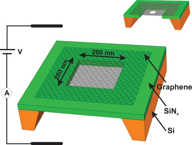
We measured the trans-electrode ionic conductance of a 0.5 × 0.5 mm, CVD grown, sheet of graphene mounted across the surface of a 200 × 200 nm aperture in a 250 nm thick, free-standing, insulating SiNx layer on a Si substrate chip (Fig. 1). Micro-Raman spectroscopy scans of the G, G' peaks from the graphene showed it to consist of a mixture of 1 and 2 atomic layer regions of graphene3,4 with ~10μ m domains. The chip-mounted membrane was inserted in a fluidic cell so that it separated two compartments, each subsequently filled with ionic solutions electrically contacted with Ag/AgCl electrodes. The small diameters of the PDMS seals in the fluidic cell precluded ionic solution from leaking around the edges of the graphene.
Figure 1. Schematic of our experiments.
A graphene membrane was mounted over a 200×200 nm2 aperture in SiNx suspended across a Si frame (not to scale). The membrane separates two ionic solutions in contact with Ag/AgCl electrodes. Inset: A graphene membrane into which a nanopore has been drilled.
With 100 mV bias applied between the two Ag/AgCl electrodes, current measurements in a variety of chloride electrolytes show that the graphene membrane's trans-conductance is far below the nS level (Table I). The highest conductances are observed for solutions with the largest atomic size cations, Cs and Rb, correlated with a minimal hydration shell that mediates their interaction with the graphene5,6. We attribute this conductance to ion transport through defect structures in the free-standing graphene. Contributions from electrochemical currents to and from the graphene can be ruled out (Methods). The observed conductances for different cations falls much faster than the solution conductivities on going from CsCl to LiCl (Table 1), suggesting an influence of graphene-cation interactions. Nevertheless we cannot completely rule out ionic transport through graphene that is in contact with the chip surface. Small asymmetries and nonlinearities in the I–V curves were observed in the data for Table 1 and elsewhere (e.g., Fig. 2), reflecting asymmetrical properties of the graphene surfaces associated with its CVD growth3 or transfer to the chip.
Table I. Trans-membrane conductivity of an as-grown graphene membrane.
The membrane separated two compartments, each containing only the ionic solutions indicated in column 1. Conductances were determined from voltage bias scans between +100 mV and −100 mV. All data shown here are from the same device whose graphene membrane was suspended across a 200 nm × 200 nm SiNx frame. The absolute magnitudes of the conductances varied by a factor of two from membrane to membrane, but the systematic variation with ionic solutions was invariant for all membranes.
| Solution | Graphene Conductance (pS) | Sol. Conductivity (10−3Sm−1) | Hydration energy20 (eV) |
|---|---|---|---|
| CsCl | 67±2 | 1.42 | 3.1 |
| RbCl | 70±3 | 1.42 | 3.4 |
| KCl | 64±2 | 1.36 | 3.7 |
| NaCl | 42± 2 | 1.19 | 4.6 |
| LiCl | 27±3 | 0.95 | 5.7 |
Figure 2. Trans-electrode I–V curves.
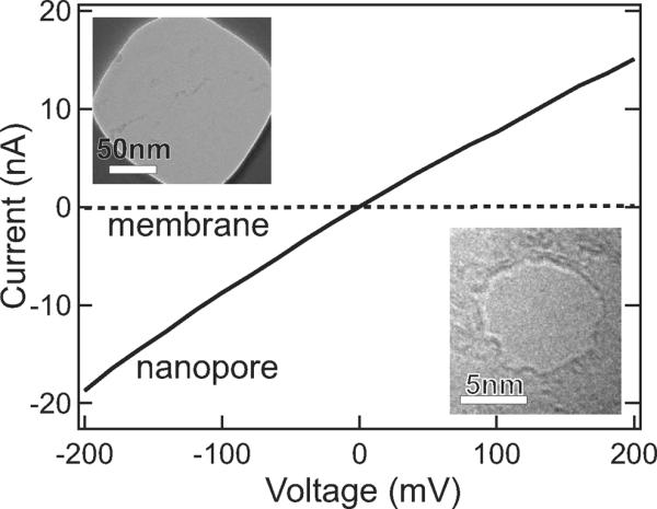
Results for an as-grown graphene membrane (dashed line) and a membrane with a 8 nm pore (solid line). The ionic conductance of the pore is quantitatively in agreement with the modeling presented in the text. Applying bias voltages in excess of ~250 mV gradually degraded the insulating properties of the membranes. Insets, top: transmission electron micrograph (TEM) of a mounted graphene membrane; bottom: TEM images of the 8 nm pore.
E-beam drilling a single nanometer scale pore7 in the graphene trans-electrode membrane increases its ionic conductivity by orders of magnitude (Fig. 2). Experiments with known nanopore diameters and solution conductivities allow one to deduce graphene's effective insulating thickness. The ionic conductance G of a pore of diameter d in an infinitely thin insulating membrane is given by8
| (1) |
where σ = F(μK + μCl)c is the conductivity of the ionic solution, F is the Faraday constant, c is ionic concentration, and μi(c) is the mobility of potassium (i = K) and chloride (i = Cl) ions used in our measurements. The linear dependence of conductance on diameter follows from the current density being sharply peaked at the pore's perimeter for an infinitely thin membrane. For membranes thicker than the pore diameter the conductivity becomes proportional to the nanopore area. For finite but small thicknesses we rely on computer calculations to predict the conductance.
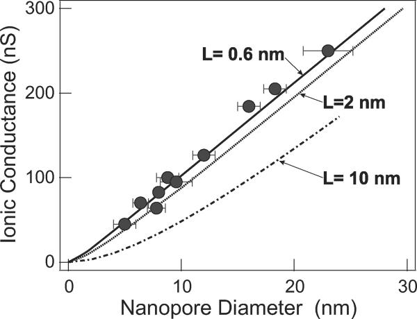
In agreement with equation (1), the trans-electrode conductivities of pores with diameters ranging from 5 to 23 nanometers (Fig. 3) exhibited a near-linear dependence on pore diameter. Fig. 3 also shows the results of computer calculations of nanopore ionic conductivity in an idealized uncharged, insulating membrane, as a function of pore diameter and membrane thickness. They are obtained by numerically solving the Laplace equation for the ionic current density, with appropriate solution conductivity and boundary conditions, and integrating over the pore area to get the conductivity (see Methods). The results are equivalent to the solution of the Poisson-Nernst-Planck equation in the same geometry. We refer to the membrane thickness L used in this idealized model as the Graphene Insulating Thickness, or LGIT. The best fit to the measured pore conductance data in Fig. 3 yields LGIT = 0.6 (+0.9−0.6) nm, with the uncertainty determined from a least square error analysis. Fig. 3 also shows the theoretical results for LGIT = 2.0 nm and LGIT = 10.0 nm.
Figure 3. Graphene nanopore conductance.
Closed circles are experimental results with a 1 M KCl solution of conductivity σ = 11 Sm−1. The solid curve shows the modeled conductance of a 0.6 nm thick insulating membrane and is the best fit to the experimentally measured conductances. Error bars represent standard deviation of 4 diameter measurements along different nanopore axes. Modeled conductances for a 2 nm thick membrane (dotted line) and a 10 nm thick membrane (dash-dot line) are presented for comparison.
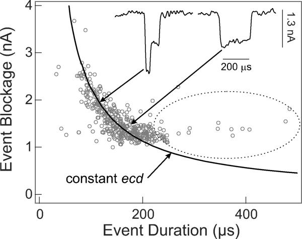
Measurements of nanopore conductivity when a long chain polymer of DNA passes through the nanopore provide an alternative method of evaluating LGIT. In such experiments, the negatively charged DNA molecules are electrophoretically drawn to and driven through a nanopore. Each insulating molecule passing through the pore transiently reduces, or blocks, the ionic conductivity in a manner that reflects both polymer size and conformation9. As shown below, such DNA experiments also reveal the membrane thickness and the nanopore diameter. The results using a 5 nm pore in graphene and double stranded DNA molecules are shown in Fig. 4. The insets show two single molecule translocation events. In the right-hand event a molecule passes through the pore in an unfolded linear fashion. In the left-hand event the molecule is folded over on itself when it enters the pore, increasing the current blockade for a short time9. Each single molecule translocation event can be characterized by two parameters: the average current drop, or blockade, and the duration of the blockade, which is the time it takes for the molecule to completely translocate through the pore. The scatter plot in Fig. 4 shows the value of these parameters for each of 400 DNA single molecule events. The characteristic shape of this data is similar to that obtained in silicon nitride nanopore experiments9 where almost all the events, folded and unfolded, fall near a line of constant electronic charge deficit (ecd), i.e. regardless of how the otherwise identical molecules are folded, each blocks the same amount of ionic charge movement through the pore during the total time it takes each molecule to move through the pore9. Such molecules pass through the pore uninhibited by sticking to the graphene surface. The few events that are encircled in the plot do not satisfy this condition and their long translocation times indicate graphene-DNA interactions, which slow their translocation through the nanopore.
Figure 4. Average nanopore current blockades vs. blockade duration during DNA translocation.
DNA (16 μg/ml) was electrophoretically driven through a 5 nm diameter graphene pore by an applied voltage bias of 160 mV. The graphene membrane separated two fluid cells containing unbuffered 3M KCl solutions, pH 10.4. Insets show typical current-time traces for two translocation events sampled from among those pointed to by the arrows. The hyperbolic curve corresponds to freely translocating events at a fixed ecd12. Encircled events are delayed by graphene DNA interactions.
We compare the experimentally determined open pore and DNA blocked pore conductance with numerical solutions (as above, and see Methods), where the membrane thickness and the nanopore diameter are the fitting parameters. Using the observed mean current blockade ΔI =1.24 ± 0.08 nA during translocation of unfolded double-stranded DNA of diameter 2.0 nm10, and the observed conductance of the pore G = 105 ± 1 nS absent DNA, we calculate that LGIT = 0.6 ± 0.5 nm, in excellent agreement with the value deduced above from open pore measurements alone. The pore diameter dGIT = 4.6±0.4 nm deduced from these calculations also agrees with the geometric diameter of 5 ± 0.5 nm obtained from a TEM of this pore.
The best fit value LGIT = 0.6 nm from both experiments agrees with molecular dynamics simulations showing the graphene-water distance to be 0.31 – 0.34 nm on each side of the membrane11,12. LGIT might also be influenced by the typical presence of immobilized water molecules and adsorbed ions in the Stern layer13. On the other hand, theoretical studies argue against any immobilized water layer on graphene, and experimental measurements support an anomalously high slip between water and an internal curved carbon nanotube surface11,14. Although very little is actually known about the surface chemistry of specifically adsorbed ions on single graphene layers1, measurements of the ionic current through the inner volume of carbon nanotubes with diameters less than 1 nm15 may indicate that ions are not immobilized on these graphitic surfaces at all. Our sub-nanometer values for LGIT support this view.
The extremely small LGIT value we obtain suggests that nanopores in graphene membranes are uniquely optimal for discerning spatial or chemical molecular structure along the length of a molecule as it passes through the pore. Although polymer translocation speeds and electronics bandwidth currently preclude a direct measurement of a nanopore's spatial or geometric resolution limit16, we can gain insight into the system's limit by numerically modeling the resolution obtainable as a function of LGIT.
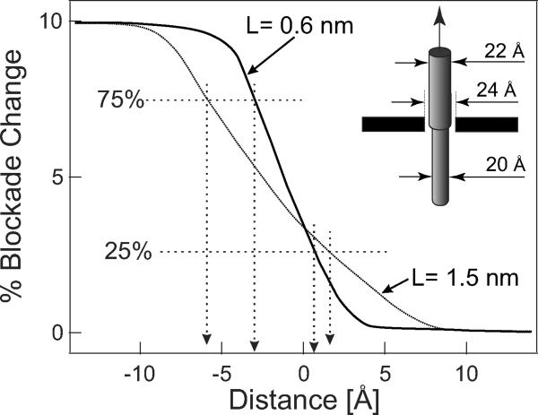
The model uses a long insulating 2.2 nm diameter cylinder symmetrically translocating through the center of a 2.4 nm diameter nanopore. At one position along its length, the cylinder diameter changes discontinuously from 2.2 nm to 2.0 nm. Solving for the conductance for this geometry as the discontinuity passes through the pore, we obtain the predictions shown in Fig. 5. The decreasing blockade (increasing conductance) of a pore is clearly seen as the large diameter portion of the cylinder exits the pore. The results of calculations for two LGIT values are shown. For the conservative LGIT = 1.5 nm, the spatial resolution (defined as the distance over which the conductivity changes from 75% of its greatest value to 25% of that value) is given by δzGIT = 7.5 Å, whereas the best-fit value LGIT = 0.6 nm leads to δzGIT = 3.5 Å. We conclude from our experiments and modeling that a pore in graphene is inherently capable of probing molecules with sub nanometer resolution. Functionalizing the graphene nanopore boundary5 or observing its local in-plane electrical conductivity during translocations may provide additional or alternative means of further increasing the resolution of this system.
Figure 5. Geometric Resolution.
Modeled nanopore conductance as the abrupt diameter decrease of a model molecule (inset) translocates through a 2.4 nm pore. The attainable resolution for two membranes of different insulating thicknesses is assumed to be achieved when the measured current through the nanopore changes from 75% to 25% of the maximum blockade change that would occur as the model molecule translocates through the nanopore.
We have demonstrated that an atomically thin sheet of graphene can be fabricated into a new structure – a transelectrode membrane – that attracts cations and anions to its opposing surfaces with sub-nanometer proximity. Interactions between anions and cations across the interface are mediated by the graphene and the high electric fields this interface supports. Due to its extreme thinness the graphene layer's in-plane electronic conductance is also sensitive and available for probing the interfacial environment. With electrical contacts applied to the graphene electrode, this conductance can be measured even for very small area (< 1×1μm) membranes, making the trans-electrode a particularly interesting device for chemical sensing and surface electrochemistry studies. Surface chemical reactions can be probed at very few charged sites by ionic current measurements through a silicon nitride nanopore17. In-plane electronic and nanopore ionic current measurements with trans-electrode devices will greatly extend this methodology. Many opportunities exist for modifying the trans-electrode device properties and sensitivity (e.g. by changing membrane thickness, doping, and defects). The interactions at, and between, the two liquid-solid interfaces in graphene may well hold many surprises and applications.
After our manuscript was submitted to Nature, the concept of using graphene nanopores to characterize DNA polymers appeared online18,19. We believe our paper provides the first realization of DNA translocation through atomically thin graphene.
Methods Summary
Graphene grown via CVD on the surface of a nickel substrate2 was spin-coated with an MMA(8.5)-MAA copolymer adhesion film. The nickel was etched away overnight in a 1 N HCl solution. The film was placed graphene side down across a 200nm square aperture in the SiNx coating on a windowed Si chip (see Fig. 1). The MMA adhesion film was dissolved and washed away with acetone. Nanometer scale pores in the graphene were e-beam drilled in a 200 keV JEOL 2010 TEM7. The fluidic cell was fashioned from PEEK with PDMS fluidic seals on each side of the chip. Ionic current measurements through the as-produced graphene membranes or graphene membranes with nanopores were performed by standard electrophysiology methods20,21.
Methods
Continuous large-scale graphene films were synthesized via chemical vapor deposition on 500 nm thick nickel film evaporated on top of Si/SiO2 wafer, using a recently published method2. Raman spectroscopy, transmission electron microscopy and selected area diffraction studies2,3 show the graphene film to be of excellent quality and mostly (87%) a mixture of 1 and 2 layer thick domains, with domain sizes of ~10 μm. Thicker regions of 3 or more graphene layers, easily distinguished by color contrast in an optical microscope, cover only a small fraction of the total surface. If thicker regions or domain boundaries were found within the 200 nm × 200 nm active region of a device, that device was discarded.
Graphene was transferred to a carrier Si/SiNx chip using a transfer technique similar to one previously published2. First, the Si/SiO2/Ni wafer with synthesized graphene was coated with MMA-MAA copolymer (MMA(8.5)MAA EL9, Microchem Corp.) and cut into 0.5 nm × 0.5 mm pieces. These pieces were immersed for ~8 hr in 1N HCl solution to etch away the Ni film and free the graphene/polymer membrane, which was transferred to distilled water on which the graphene/polymer floated, graphene-side down. A carrier Si chip coated with ~250 nm thick SiNx was used to scoop up the floating graphene/polymer film, taking care that the graphene/polymer film was stretched over the central region of the chip. The central region of the chip had been microfabricated using standard anisotropic etch techniques to leave a ~50×50 μm2 area of the SiNx coating as a free-standing SiNx membrane into which a square window, ~200 nm × 200 nm had been drilled using a focused ion beam (FIB). Nitrogen gas flow was used to firmly press the graphene against the chip's surface. This led to expulsion of a small amount of liquid from under the graphene, which adhered strongly and irreversibly to the carrier chip's SiNx coating. The polymer on top of the graphene was removed under a slow drip of acetone, followed by subsequent immersions in acetone, dicholoroethane, and finally isopropanol.
To remove any residues from the graphene film, the chip was subsequently immersed in 33 wt% solution of KOH at room temperature for 1min, then vigorously rinsed with isopropanol and ethanol. To avoid damage to the suspended free-standing portion of the graphene film, the chip was critical-point dried. Finally, the chip was loaded into a rapid thermal annealer and heated to 450°C in a stream of gas containing 4% H2 in He for 20 minutes to drive off any remaining hydrocarbons. To avoid recontamination, the chip was immediately loaded into a transmission electron microscope for further processing.
A single nanometer-sized pore was drilled through the graphene membrane using a focused electron beam in a JEOL 2010 FEG transmission electron microscope operated at 200kV acceleration voltage. Methods to form more reproducibly dimensioned nanopores in graphene are being developed, but we determined the nanopore size by EM visualization in a well spread electron beam so as to keep the total electron exposure of the graphene membrane to a minimum. The reported nanopore diameter is an average of 4 measurements along different nanopore axes, as determined from calibrated TE micrographs using DigitalMicrograph software (Gatan, Inc.). The error bar represents the standard deviation of those measurements, and reflects irregularities and deviations of the pore perimeter from perfect circularity. If the chip or TEM holder had any contaminating organic residue, amorphous carbon was seen to visibly deposit under the electron beam. Such devices were discarded. After drilling the nanopore, the graphene nanopore chips that were not immediately investigated were kept under a clean vacuum of ~10−5 Torr.
The chip-mounted graphene was inserted between the two half-cells of a custom-built microfluidic cassette made of polyether-etherketone (PEEK). The two sides of the chip were sealed with polydimethylsiloxane (PDMS) gaskets. The opening of the gasket that pressed against the graphene film on the Si/SiNx carrier chip (see Fig. 1) had an inside diameter of ~100 μm. Consequently, the gasket orifice was smaller than the dimensions of the graphene film (0.5×0.5 mm2), and completely sealed off the graphene edge from the electrolyte. On the opposite side of the chip, the electrolyte is in contact with the graphene membrane only through the 200 nm wide square window in SiNx membrane. Note that there is a large area difference between the two graphene faces in contact with the electrolyte (a circular area of 100 μm diameter vs. a square 200 nm × 200 nm area). This difference in contact area may in part explain the small conductance asymmetries and nonlinearities in our graphene I–V curves.
The two half-cells were first filled with ethanol to facilitate wetting of the chip surface. The cell was then flushed with deionized water, followed by 1M KCl salt solution with no buffer. To avoid any potential interaction between the graphene and the solutes which could affect the measurements of graphene thickness and DNA translocations, all the electrolytes were kept as simple as possible and were unbuffered. With the exception of solutions used in the experiment of Fig. 4, all solution pHs ranged only 0.2 pH units, from 5.09 to 5.29, as measured both before and after use in the described experiments. The pH of the solution used for the Fig. 4 experiment was adjusted to pH 10.4 with KOH just before use. Because the design of our microfludic cassette maintained the solution largely out of contact with ambient atmosphere, the pH varied less than 0.2 pH units during the course of the Fig. 4 experiments.
Ag/AgCl electrodes in each half-cell were used to apply an electric potential across the graphene membranes and to measure ionic currents. The current traces were acquired using an Axopatch 200B (Axon instruments) amplifier, which was connected to an external 8-pole Bessel low-pass filter (type 90IP-L8L, Frequency Devices, Inc.) operating at 50 kHz. The analog signal was digitized using a NI PCI-6259 DAQ card (National Instruments) operating at 250 kHz sampling rate and 16-bit resolution. The experiment was controlled through IGOR Pro software.
For DNA translocation measurements, the microfluidic cell was flushed with 3M KCl salt solution at pH 10.4, containing 1mM EDTA. High salt concentration and high pH were found to minimize DNA-graphene interaction. We introduced 10kbp restriction fragments of double stranded lambda DNA molecules to the cis chamber. The DNA translocation events were analyzed with MATLAB using a fitting function that consisted of multiple square pulses convoluted with an appropriate Bessel filter function to mimic the recording conditions.
Conductivities of all the solutions mentioned in the manuscript were measured using Accumet Research AR50 conductivity meter, which had been calibrated using conductivity standard solutions (Alfa Aesar, product #43405, 42695, 42679). All the fluidic experiments were performed under temperature controlled laboratory conditions, at 24°C.
To investigate the contribution from electrochemical (Faradic) currents, a large-area graphene film (~2×4 mm2) was transferred to a glass slide and contacted at one end with silver paint attached to a metallic clip over which wax insulation was placed. The exposed end of the film was immersed in 1M KCl electrolyte with a Ag/AgCl counter electrode, and the electrochemical I–V curves were measured in the same voltage range as used in the trans-electrode experiments. After normalizing for the surface area, we conclude that any electrochemical currents in the trans-electrode devices were 3 orders of magnitude too small to account for the ~pA currents measured through the as-grown graphene membranes in Table 1.
The numerical simulations were performed using COMSOL Multiphysics finite element solver in appropriate 3D geometry with cylindrical symmetry along the axis of the nanopore. We solved the full set of Poisson-Nerst-Planck equations in the steady-state regime. In the range of physical parameters of interest (high salt concentration and small applied voltage), the numerical simulation solution was found not to differ significantly from the solution of the Laplace equation with fixed conductance, which has significantly less computational penalty. A DNA molecule was modeled as a long stiff insulating rod of diameter 2 nm which threads through the center of the nanopore. For lateral resolution calculations, we added a step of 2.2 nm in diameter to the DNA model, and we calculated the change in the ionic current as the discontinuity is translocated through the center of the pore. The total electrical current was calculated by integrating current density across the diameter of the nanopore.
Acknowledgements
This work was funded by a grant to J.A.G. and D.B. from the National Human Genome Research Institute, National Institutes of Health.
References
- 1.Geim AK. Graphene: Status and prospects. Science. 2009;324:1530–1534. doi: 10.1126/science.1158877. [DOI] [PubMed] [Google Scholar]
- 2.Reina A, et al. Large area, few-layer graphene films on arbitrary substrates by chemical vapor deposition. Nano Lett. 2009;9:30–35. doi: 10.1021/nl801827v. [DOI] [PubMed] [Google Scholar]
- 3.Reina A, et al. Growth of large-area single- and bi-layer graphene by controlled carbon precipitation on polycrystalline Ni surfaces. Nano Res. 2009;2:509–516. [Google Scholar]
- 4.Ferrari AC, et al. Raman spectrum of graphene and graphene layers. Phys. Rev. Lett. 2006;97:187401. doi: 10.1103/PhysRevLett.97.187401. [DOI] [PubMed] [Google Scholar]
- 5.Sint K, Wang B, Kral P. Selective ion passage through functionalized graphene nanopores. J. Am. Chem. Soc. 2008;130:16448–16449. doi: 10.1021/ja804409f. [DOI] [PubMed] [Google Scholar]
- 6.Zwolak M, Lagerqvist J, Di Ventra M. Quantized ionic conductance in nanopores. Phys. Rev. Lett. 2009;103:128102. doi: 10.1103/PhysRevLett.103.128102. [DOI] [PMC free article] [PubMed] [Google Scholar]
- 7.Storm AJ, Chen JH, Ling XS, Zandbergen HW, Dekker C. Fabrication of solid-state nanopores with single-nanometre precision. Nature Materials. 2003;2:537–541. doi: 10.1038/nmat941. [DOI] [PubMed] [Google Scholar]
- 8.Hall JE. Access resistance of a small circular pore. The Journal of General Physiology. 1975;66:531–532. doi: 10.1085/jgp.66.4.531. [DOI] [PMC free article] [PubMed] [Google Scholar]
- 9.Li J, Gershow M, Stein D, Brandin E, Golovchenko J. DNA molecules and configurations in a solid-state nanopore microscope. Nature Materials. 2003;2:611–615. doi: 10.1038/nmat965. [DOI] [PubMed] [Google Scholar]
- 10.Zwolak M, DiVentra M. Physical approaches to DNA sequencing and detection. Reviews of Modern Physics. 2008;80:141–165. [Google Scholar]
- 11.Alexiadis A, Kassinos S. Molecular simulation of water in carbon nanotubes. Chem. Rev. 2008;108:5014–5034. doi: 10.1021/cr078140f. [DOI] [PubMed] [Google Scholar]
- 12.Werder T, Walther JH, Jaffe RL, Halicioglu T, Koumoutsakos P. On the water-carbon interaction for use in molecular dynamics simulations of graphite and carbon nanotubes. J. Phys. Chem. B. 2003;107:1345–1352. [Google Scholar]
- 13.Bard AJ, Faulkner LR. Electrochemical Methods. Fundamentals and Applications. 2ed. John Wiley & Sons; New York: 2001. [Google Scholar]
- 14.Holt JK, et al. Fast mass transport through sub-2-nanometer carbon nanotubes. Science. 2006;312:1034–1037. doi: 10.1126/science.1126298. [DOI] [PubMed] [Google Scholar]
- 15.Liu H, et al. Translocation of single-stranded DNA through single-walled carbon nanotubes. Science. 2010;327:64–67. doi: 10.1126/science.1181799. [DOI] [PMC free article] [PubMed] [Google Scholar]
- 16.Branton D, et al. The potential and challenges of nanopore sequencing. Nature Biotechnology. 2008;26:1146–1153. doi: 10.1038/nbt.1495. [DOI] [PMC free article] [PubMed] [Google Scholar]
- 17.Hoogerheide DP, Garaj S, Golovchenko JA. Probing surface charge fluctuations with solid-state nanopores. Phys. Rev. Lett. 2009;102:2568041–2568044. doi: 10.1103/PhysRevLett.102.256804. [DOI] [PMC free article] [PubMed] [Google Scholar]
- 18.Schneider GF, et al. DNA translocation through graphene nanopores. Nano Lett. 2010 doi: 10.1021/nl102069z. ASAP article; DOI: 10.1021/nl102069z. [DOI] [PubMed] [Google Scholar]
- 19.Merchant CA, et al. DNA translocation through graphene nanopores. Nano Lett. 2010 doi: 10.1021/nl101046t. ASAP article; DOI: 10.1021/nl101046t. [DOI] [PubMed] [Google Scholar]
- 20.Hille B. Ion channels of excitable membranes. 3rd edition Sinauer Associates; Sunderland, MA: 2001. [Google Scholar]
- 21.Kasianowicz JJ, Brandin E, Branton D, Deamer DW. Characterization of individual polynucleotide molecules using a membrane channel. Proc. Natl. Acad. Sci. U.S.A. 1996;93:13770–13773. doi: 10.1073/pnas.93.24.13770. [DOI] [PMC free article] [PubMed] [Google Scholar]


