

Abstract
Graphene has attracted considerable interest as a potential new electronic material1–11. With the highest carrier mobility exceeding 200,000 cm2/V·s, graphene is of particular interest for ultra-high speed radio frequency (RF) electronics12–18. However, the conventional dielectric integration and device fabrication processes cannot be readily applied to fabricate high speed graphene transistors because they can often introduce significant defects into the monolayer of carbon lattices and severely degrade the device performance19–21. Here we report a new approach to fabricate high-speed graphene transistors with a self-aligned nanowire gate to enable unprecedented performance. The graphene transistors are fabricated using a Co2Si/Al2O3 core/shell nanowire as the gate, with the source and drain electrodes defined through a self-alignment process and the channel length defined by the nanowire diameter. The physical assembly of nanowire gate preserves the high carrier mobility in graphene, and the self-aligned process ensures that the edges of the source, drain, and gate electrodes are automatically and precisely positioned so that no overlapping or significant gaps exist between these electrodes and thus minimizes access resistance. It therefore enables transistor performance not previously possible. Graphene transistors with channel length down to 140 nm have been fabricated with the highest scaled on-current (3.32 mA μm−1) and transconductance (1.27 mS μm−1) reported to date. Significantly, on-chip microwave measurements demonstrate that the self-aligned devices exhibit a record high intrinsic cutoff frequency (fT) in the range of 100–300 GHz, with the extrinsic fT in the range of a few gigahertz largely limited by parasitic pad capacitance. The reported intrinsic cutoff frequency of the graphene transistors is comparable to that of the very best high electron mobility transistors with similar gate lengths10. It therefore marks an important milestone in graphene RF devices and can enable exciting opportunities in high-speed electronics.
With the highest carrier mobility exceeding 200,000 cm2/V·s8, and many other desirable properties including large critical current densities (~2×10⁸ A/cm2)22 and a high saturation velocity (5.5×107 cm/s)11, graphene is of significant potential for high speed electronics to offer excellent RF characteristics with very high cutoff frequency (fT). Importantly, recent studies have demonstrated graphene transistors operating in the gigahertz regime12–14,16–18 with a record of fT =100 GHz13. The reported RF performance to date is however still far from the potential that the graphene transistors may offer, primarily limited by two adverse factors in the device fabrication process.
A first limitation is associated with the severe mobility degradation resulted from graphene-dielectric integration process that introduces substantial defects into pristine graphene lattices20,23. To this end, we have recently developed a new strategy to integrate high quality high-k dielectrics with graphene using a physical assembly approach without introducing any appreciable defects into the graphene lattices, and demonstrated the top-gated graphene transistors with the highest carrier mobility exceeding 20,000 cm2/V·s24–26. Another limitation of the top-gated graphene transistors reported to date is the large access resistance due to non-optimum alignment of the source-drain and gate electrodes, which can have particularly adverse impact on short channel devices. With decreasing channel length, there is an increasing demand for a more precise device fabrication process. In the state-of-the-art silicon MOSFET technology, a self-aligned gate structure is used to ensure that the edges of the source, drain, and gate electrodes are precisely positioned so that no overlapping or significant gaps exist between these electrodes. However, these conventional dielectric integration and device fabrication processes used in silicon technology can not be readily employed for graphene-based electronics, as many of them can lead to significant damages in the monolayer of graphene lattices with severe performance degradation.
Here we report an entirely new strategy to fabricate graphene transistors using a Co2Si/Al2O3 core/shell nanowire as the self-aligned top-gate (Figure 1). To fabricate the device, graphene flakes were first mechanically peeled onto a highly resistive silicon substrate (> 18,000 ohm·cm) with a 300 nm thermal silicon oxide. The Co2Si/Al2O3 core/shell nanowires were aligned on top of the graphene through a physical dry transfer process25,26, followed by e-beam lithography, buffered oxide etching to remove the Al2O3 shell and expose the Co2Si core, and metallization (Ti/Au, 70/50 nm) process to define the external source, drain and gate electrodes. A thin layer of Pt metal (10 nm) was then deposited on top of the graphene across the Co2Si/Al2O3 core/shell nanowire, in which the Co2Si/Al2O3 core/shell nanowire separates the Pt thin film into two isolated regions that form the self-aligned source and drain electrodes precisely positioned next to the nanowire gate. In this device, the Co2Si/Al2O3 core/shell nanowire defines the channel length, with the 5 nm Al2O3 shell functioning as the gate dielectrics, and the metallic Co2Si core functioning as the local top-gate, and self-aligned Pt thin film pads as the source and drain electrodes (Fig. 1a, b).
Figure 1. Schematic illustration of a high-speed graphene transistor with a Co2Si/Al2O3 core/shell nanowire as the self-aligned top-gate.
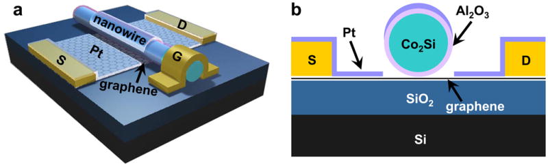
a, Schematic illustration of the three-dimensional view of the device layout. b, Schematic illustration of the cross-sectional view of the device. In this device, the Co2Si/Al2O3 core/shell nanowire defines the channel length, with the 5 nm Al2O3 shell in functioning as the gate dielectrics, and the metallic Co2Si core functioning as the self-integrated local gate, and the self-aligned Pt thin film pads as the source and drain electrodes
The Co2Si nanowires were synthesized through a chemical vapour deposition (CVD) process with the diameters typically in the range of 100–300 nm and the lengths around 10 μm (Fig. 2a)27. The composition of Co2Si was characterized by energy-dispersive x-ray spectroscopy (Supplementary Fig. S1). The Co2Si/Al2O3 core/shell nanowires were grown through atomic layer deposition (ALD) of Al2O3 shell on the Co2Si nanowires with controlled thickness. The relative dielectric constant of the ALD Al2O3 is determined to be ~7.5 based on capacitance-voltage measurement using a planar metal/Al2O3/Si control structure. Transmission electron microscope (TEM) image shows a uniform coating of the amorphous Al2O3 (light contrast) surrounding the single-crystalline Co2Si core (dark contrast) (Fig. 2b). High resolution TEM image clearly shows the single crystalline Co2Si core with an amorphous Al2O3 shell of lighter contrast (Supplementary Fig. S2). The electrical measurement of a Co2Si nanowire clearly shows linear current-voltage (I–V) characteristics (Fig. 2c) with the resistance of a 180 nm diameter and 3 micron long Co2Si nanowire close to 527 ohm, and an estimated resistivity of 437 μΩ·cm. Our measurements of over 10 nanowires give a resistivity range of 200–500 μΩ·cm, consistent with previous report27. The low resistance of the Co2Si nanowires is particularly important for them to function as effective gate electrodes for RF graphene transistors.
Figure 2. Characterization of Co2Si and Co2Si/Al2O3 core/shell nanowires.

a, SEM image of the Co2Si nanowires. The nanowires were synthesized through a chemical vapour deposition process with the diameters typically in the range of 100–300 nm and the lengths around 10 μm. b, TEM image of a Co2Si/Al2O3 core/shell nanowire shows a uniform coating of the amorphous Al2O3 (light contrast) surrounding the single-crystal Co2Si core (dark contrast). c, The I–V characteristic of a single Co2Si nanowire in two- and four-terminal measurements to determine the nanowire resistance and resistivity. The inset shows an SEM image of the device, the scale bar is 3 μm.
Figure 3a shows an SEM image of a self-aligned graphene transistor and an optical microscope image of the overall device layout (inset, Fig 3a). The cross-sectional SEM image of a typical device shows the self-aligned Pt thin film source and drain electrodes are well separated by the nanowire gate and precisely positioned next to the nanowire gate (Fig. 3b), clearly demonstrating that the self-alignment process can be used to effectively integrate graphene with a nanowire gate and nearly perfectly positioned source and drain electrodes.
Figure 3. Room temperature electrical characteristics of the graphene transistors with a self-aligned nanowire gate.

a, An SEM images of a graphene transistor with a self-aligned nanowire gate, the width of devices of about 2.64 μm. The inset shows an optical microscope image the overall device layout. b, The cross-sectional SEM image of a typical device shows the self-aligned Pt thin film source and drain electrodes are well separated by the nanowire gate and precisely positioned next to the nanowire gate. The graphene below the nanowire gate is not clearly visible. c, and d, Ids-VTG transfer characteristics at Vds = −1 V before and after the deposition of the self-aligned Pt source-drain electrodes. e, The Ids-Vds output characteristics at various gate voltages (VTG =0.0, 0.4, 0.8, 1.2, 1.6, and 2.0 V) for the dIds self-aligned device. f, Transconductance at Vds = −1 V as a function of top-gate voltage VTG before (black) and after (red) the deposition of the self-aligned Pt source-drain electrodes, highlighting the self-alignment process increases the peak transconductance by a factor of > 60. g, Two dimensional plot of the device conductance for varying VBG and VTG bias for self aligned device. The unit in the color scale is mS. h, The top-gate Dirac point VTG_Dirac at different VBG, with which we can derive CTG/CBG≈38.
Prior to the formation of the self-aligned Pt source and drain electrodes, we have measured the transfer characteristics, drain-source current (Ids) versus top-gate voltage (VTG)applied by the local nanowire gate. The Ids -VTG plot clearly shows that the graphene transistor can be modulated by the local nanowire gate, overturning from the hole branch to electron branch within −1 to 3 V range (Fig. 3c), demonstrating the Co2Si/Al2O3 core/shell nanowire can indeed function as an effective local gate for the graphene transistors. However, the gate modulation is less than 10%, smaller than the typical values observed in graphene transistors at room temperature (around 50%). This difference can be attributed to the large access resistance due to the relatively small gated area compared to the entire graphene channel.
The formation of the self-aligned source and drain electrodes allows precise positioning of the source-drain edges with the gate edges, and thus substantially reduce the access resistance and improve the graphene transistor performance. Before transistor characterization of the self-aligned devices, we have first tested the gate leakage across the Co2Si/Al2O3/graphene gate stack. The gate tunnelling leakage current (Igs) from the Co2Si/Al2O3 core/shell nanowire to the underlying graphene is negligible within the gate voltage range of ± 3 V range (Supplementary Fig. S3). This measurement demonstrates that the 5 nm Al2O3 dielectrics can function as an effective gate insulator for top-gated graphene transistors and afford high gate capacitance that is critical to the high transconductance.
Importantly, the Ids-VTG transfer curve recorded for a self-aligned device shows a current modulation of about 42 % (Fig. 3d), comparable to the typical values observed in long channel graphene transistors, suggesting that the access resistance in this ultra-short channel device is largely removed through the self-alignment process. The hysteresis of Ids-VTG is about 0.02 V under ambient conditions (Supplementary Fig. S4), demonstrating the relative clean nature of the graphene-dielectric interface. Figure 3e shows the Ids-Vds output characteristics at various gate voltages. The device can deliver a maximum scaled on-current of 3.32 mA/μm at Vds = −1 V and VTG = −1 V. The transconductance can be extracted from the Ids-VTG curve (Fig. 3f). A peak scaled transconductance of 0.02 mS/μm is obtained at Vds = −1 V for the device prior to the deposition of the self-aligned source and drain electrodes. Significantly, with the self-aligned source and drain electrodes, the peak scaled transconductance at Vds = −1 V reaches 1.27 mS/μm, a more than 60 times of improvement over the non-self-aligned device. This study clearly demonstrates the self-alignment process is a critical to ensure high transistor performance in the short channel devices. To the best of our knowledge, these scaled on-current and transconductance values obtained here represent the highest values reported in bulk graphene transistors to date11–13,15–17,28. Higher transconductance was only observed previously in graphene nanoribbon transistors with much larger gate capacitance25.
To characterize the gate capacitance, we have measured the device conductance as a function of both VTG and back-gate bias (VBG) (Fig. 3g). From these measurements, we can obtain Dirac point shifts in the top-gated configuration as a function of the applied VBG (Fig. 3h), which gives the ratio between top-gate and back-gate capacitances, CTG/CBG ≈ 38. Using the back-gate capacitance value of CBG = 11.5 nF/cm2, the top-gate capacitance is estimated to be CTG = 437 nF/cm11,24, which is consistent with the results obtained from the finite element calculations, CTG = ~ 394 nF/cm2 (Supplementary Fig. S5).
The above discussions clearly demonstrate our self-aligned nanowire gate can allow us to achieve graphene transistors with unprecedented DC performance. An important benchmark of the transistor RF performance is the cutoff frequency fT. To assess the RF characteristics of our self-aligned transistors, on-chip microwave measurements were carried out in the range of 50 MHz to 30 GHz using an Agilent 8722ES network analyzer. Due to the extremely small dimension of our devices, the gate capacitance of our device is typically about two orders of smaller than the parasitic pad capacitance. To accurately determine the fT values requires careful de-embedding procedures (see Methods)13,14,17.
Figure 4a shows the current gain |h21| derived from the measured S-parameters at VTG = 1 V and a drain bias Vds = −1 V. It displays the typical 1/f frequency dependence expected for an ideal FET, yielding a fT of 300 GHz. We also verified fT data using Gummel’s approach29, in which the extracted fT is identical to the aforementioned value (inset, Fig. 4a). This extracted fT value is also consistent with the projected value (323 GHz) using the well-known relation fT = gm/(2πCg) established for conventional FETs30. Importantly, the speed of this self-aligned graphene device represents the highest in all graphene devices reported to date12–14,16–18. Furthermore, it is about two times faster than that of the best silicon MOSFETs of comparable sizes (e.g. about 150 GHz for a 150 nm Si-MOSFET), and comparable to those of the very best InP high electron mobility transistors (HEMT) and GaAs metamorphic HEMT with similar channel lengths10. Figure 4b and 4c further show the results obtained from another two self-aligned graphene transistors with a 182 nm and 210 nm nanowire gate, displaying a fT of 168 GHz and 125 GHz, respectively, also higher than any graphene transistors reported previously.
Figure 4. Measured small-signal current gain |h21| as a function of frequency f at Vds = −1 V.

a, For a device with gate length = 144 nm at VTG = 1 V; b, For a device with gate length = 182 nm at VTG = 0.3 V; and c, For a device with gate length = 210 nm at VTG = 1.1 V; These different VTG values used are the peak transconductance points for each device. The insets show the fT extraction by Gummel’s method.
It should be noted that the record high intrinsic fT values reported here are obtained after careful de-embedding procedures using the exact contact pad layout. Without de-embedding procedures, the extrinsic fT values (2.4, 1.9 and 1.6 GHz) for the three devices described above are substantially lower (Supplementary Fig. S6), due largely to the large ratio between parasitic and gate capacitance. The large intrinsic/extrinsic fT ratios (125, 88 and 78) call for further scrutiny and validation of our de-embedding procedures. To this end, we have carefully analyzed the second device to extract all device component values based on the equivalent circuit and S-parameter measurements (Supplementary Fig. S7). Importantly, the device component values (including parasitic capacitance, gate capacitance and transconductance etc.) derived from the RF measurements are consistent with those obtained from the DC measurements or electrostatic simulations (Table S1 & S2). In particular, this analysis confirms that the difference between intrinsic and extrinsic fT can be primarily attributed to the large ratio between parasitic pad capacitance and gate capacitance. Significantly, by re-designing the device layout to reduce the parasitic capacitance, we can significantly reduce the parasitic/gate capacitance ratio and hence the intrinsic/extrinsic fT ratio (Supplementary Fig. S8). These studies unambiguously validate our de-embedding procedures.
In summary, we have described a novel self-aligned process to fabricate graphene transistors with a nanowire gate. The unique device layout ensures that the edges of the source, drain, and gate electrodes are precisely and automatically positioned so that no overlapping or significant gaps exist between these electrodes. The fabrication approach allows integration of the top-gate electrodes without introducing appreciable damage into pristine graphene lattices and thus retains the high electronic performance, to enable graphene transistors with several significant advantages, including record high driving current, transconductance and fT. This study marks an important milestone in the development of high-speed graphene transistors, and opens the exciting potential of graphene-transistors in high-speed high-frequency electronics. With further optimization of graphene growth over large area, nanowire assembly or soft lithography process to precisely control the dimension and location of the self-aligned gate, large arrays of self-aligned high-speed graphene transistors or circuits can be envisioned.
METHODS SUMMARY
The Co2Si nanowires were synthesized through a chemical vapour deposition process, and Co2Si/Al2O3 core/shell nanowires by atomic layer deposition (ALD) of Al2O3 shell on the Co2Si nanowires. Graphene flakes were first mechanically peeled onto a highly resistive silicon substrate (> 18,000 ohm·cm) with a 300 nm thermal silicon oxide. The Co2Si/Al2O3 core/shell nanowires were aligned on top of the graphene through a physical dry transfer process, followed by e-beam lithography, buffered oxide etching to remove the Al2O3 shell and expose the Co2Si core, and metallization (Ti/Au, 70/50 nm) process to define the source, drain and gate electrodes. A thin layer of Pt metal (10 nm) was then deposited on top of the graphene across the Co2Si/Al2O3 core/shell nanowire, in which the Co2Si/Al2O3 core/shell nanowire separates the Pt thin film into two isolated regions that form the self-aligned source and drain electrodes precisely positioned in close proximity to the nanowire gate. The DC electrical transport studies were conducted with a probe station at room temperature under ambient conditions with a computer-controlled analogue-to-digital converter. The on-chip microwave measurements were carried out in the range of 50 MHz to 30 GHz using an Agilent 8722ES network analyzer. The measured S-parameters were de-embedded using specific “short” and “open” structures with identical layouts, excluding the graphene channel, to remove the effects of the parasitic capacitance, resistance and inductance associated with the pads and connections. The “through” calibration was done with exact pad layout with gate shorted to drain, and the “load” calibration was done with standard calibration pad.
Supplementary Material
Acknowledgments
We acknowledge A. Jooyaie and S. Martin for helpful discussions. We also acknowledge Electron Imaging Center for Nanomachines (EICN) at UCLA for the technical support of TEM, Nanoelectronics Research Facility at UCLA for technical support of device fabrication. X.D. acknowledges financial support by NSF CAREER award 0956171 and partial support by the NIH Director’s New Innovator Award Program, part of the NIH Roadmap for Medical Research, through grant number 1DP2OD004342-01.
Footnotes
Supplementary Information accompanies the paper on www.nature.com/nature.
Author Contributions X.D conceived the research. X.D. and L.L. designed the experiment. L.L. performed all the experiments including material synthesis, device fabrication, DC/RF characterization, and data analysis. Y-C.L. contributed to material synthesis, material and device structure characterization, and RF analysis. M.B. contributed to RF characterization and analysis. R.C. and Y.L. contributed to DC/RF analysis. J.B. contributed to device fabrication. Y.Q. contributed to material synthesis. X.D. and L.L. co-wrote the paper. All authors discussed the results and commented on the manuscript.
Author Information The authors declare no competing financial interests.
References
- 1.Novoselov KS, et al. Electric field effect in atomically thin carbon films. Science. 2004;306:666–669. doi: 10.1126/science.1102896. [DOI] [PubMed] [Google Scholar]
- 2.Novoselov KS, et al. Two-dimensional gas of massless Dirac fermions in graphene. Nature. 2005;438:197–200. doi: 10.1038/nature04233. [DOI] [PubMed] [Google Scholar]
- 3.Zhang YB, Tan YW, Stormer HL, Kim P. Experimental observation of the quantum Hall effect and Berry’s phase in graphene. Nature. 2005;438:201–204. doi: 10.1038/nature04235. [DOI] [PubMed] [Google Scholar]
- 4.Bunch JS, Yaish Y, Brink M, Bolotin K, McEuen PL. Coulomb oscillations and Hall effect in quasi-2D graphite quantum dots. Nano Letters. 2005;5:287–290. doi: 10.1021/nl048111+. [DOI] [PubMed] [Google Scholar]
- 5.Berger C, et al. Electronic confinement and coherence in patterned epitaxial graphene. Science. 2006;312:1191–1196. doi: 10.1126/science.1125925. [DOI] [PubMed] [Google Scholar]
- 6.Avouris P, Chen ZH, Perebeinos V. Carbon-based electronics. Nat Nanotech. 2007;2:605–615. doi: 10.1038/nnano.2007.300. [DOI] [PubMed] [Google Scholar]
- 7.Miao F, et al. Phase-coherent transport in graphene quantum billiards. Science. 2007;317:1530–1533. doi: 10.1126/science.1144359. [DOI] [PubMed] [Google Scholar]
- 8.Bolotin KI, et al. Ultrahigh electron mobility in suspended graphene. Solid State Commun. 2008;146:351–355. [Google Scholar]
- 9.Geim AK, Novoselov KS. The rise of graphene. Nat Mater. 2007;6:183–191. doi: 10.1038/nmat1849. [DOI] [PubMed] [Google Scholar]
- 10.Schwierz F. Graphene transistors. Nature Nanotech. 2010;5:487–496. doi: 10.1038/nnano.2010.89. [DOI] [PubMed] [Google Scholar]
- 11.Meric I, et al. Current saturation in zero-bandgap, topgated graphene field-effect transistors. Nat Nanotech. 2008;3:654–659. doi: 10.1038/nnano.2008.268. [DOI] [PubMed] [Google Scholar]
- 12.Lin YM, et al. Dual-gate graphene FETs with f(T) of 50 GHz. IEEE Electron Dev Lett. 2010;31:68–70. [Google Scholar]
- 13.Lin YM, et al. 100-GHz transistors from wafer-scale epitaxial graphene. Science. 2010;327:662–662. doi: 10.1126/science.1184289. [DOI] [PubMed] [Google Scholar]
- 14.Meric I, Baklitskaya N, Kim P, Shepard KL. RF performance of top-gated, zero-bandgap graphene field-effect transistors. Tech Dig IEDM. 2008;4 [Google Scholar]
- 15.Farmer DB, et al. Utilization of a buffered dielectric to achieve high field-effect carrier mobility in graphene transistors. Nano Lett. 2009;9:4474–4478. doi: 10.1021/nl902788u. [DOI] [PubMed] [Google Scholar]
- 16.Jeon DY, et al. Radio-frequency electrical characteristics of single layer graphene. Jpn J Appl Phys. 2009;48:091601. [Google Scholar]
- 17.Lin YM, et al. Operation of graphene transistors at gigahertz frequencies. Nano Lett. 2009;9:422–426. doi: 10.1021/nl803316h. [DOI] [PubMed] [Google Scholar]
- 18.Moon JS, et al. Epitaxial-graphene RF field-effect transistors on Si-face 6H-SiC substrates. IEEE Electron Dev Lett. 2009;30:650–652. [Google Scholar]
- 19.Lee BK, et al. Conformal Al2O3 dielectric layer deposited by atomic layer deposition for graphene-based nanoelectronics. Appl Phys Lett. 2008;92:203102. [Google Scholar]
- 20.Wang XR, Tabakman SM, Dai HJ. Atomic layer deposition of metal oxides on pristine and functionalized graphene. J Am Chem Soc. 2008;130:8152–8153. doi: 10.1021/ja8023059. [DOI] [PubMed] [Google Scholar]
- 21.Xuan Y, et al. Atomic-layer-deposited nanostructures for graphene-based nanoelectronics. Appl Phys Lett. 2008;92:013101. [Google Scholar]
- 22.Murali R, Yang YX, Brenner K, Beck T, Meindl JD. Breakdown current density of graphene nanoribbons. Appl Phys Lett. 2009;94:243114. [Google Scholar]
- 23.Ni ZH, et al. Tunable stress and controlled thickness modification in graphene by annealing. ACS Nano. 2008;2:1033–1039. doi: 10.1021/nn800031m. [DOI] [PubMed] [Google Scholar]
- 24.Liao L, et al. High-kappa oxide nanoribbons as gate dielectrics for high mobility top-gated graphene transistors. Proc Natl Acad Sci USA. 2010;107:6711–6715. doi: 10.1073/pnas.0914117107. [DOI] [PMC free article] [PubMed] [Google Scholar]
- 25.Liao L, et al. Top-gated graphene nanoribbon transistors with ultrathin high-k dielectrics. Nano Lett. 2010;10:1917–1921. doi: 10.1021/nl100840z. [DOI] [PMC free article] [PubMed] [Google Scholar]
- 26.Liao L, et al. High-performance top-gated graphene-nanoribbon transistors using zirconium oxide nanowires as high-dielectric-constant gate dielectrics. Adv Mater. 2010;22:1941–1945. doi: 10.1002/adma.200904415. [DOI] [PMC free article] [PubMed] [Google Scholar]
- 27.Seo K, et al. Composition-tuned ConSi nanowires: location-selective simultaneous growth along temperature gradient. ACS Nano. 2009;3:1145–1150. doi: 10.1021/nn900191g. [DOI] [PubMed] [Google Scholar]
- 28.Lemme MC, Echtermeyer TJ, Baus M, Kurz H. A graphene field-effect device. IEEE Electron Dev Lett. 2007;28:282–284. [Google Scholar]
- 29.Kim DH, del Alamo JA. 30-nm InAs pseudomorphic HEMTs on an InP substrate with a current-gain cutoff frequency of 628 GHz. IEEE Electron Dev Lett. 2008;29:830–833. [Google Scholar]
- 30.Sze SM, Ng KK. Physics of Semiconductor Devices. Wiley-Interscience; 2007. [Google Scholar]
Associated Data
This section collects any data citations, data availability statements, or supplementary materials included in this article.