

Abstract
We present the design for OpenPET, an electronics readout system designed for prototype radiotracer imaging instruments. The critical requirements are that it has sufficient performance, channel count, channel density, and power consumption to service a complete camera, and yet be simple, flexible, and customizable enough to be used with almost any detector or camera design. An important feature of this system is that each analog input is processed independently. Each input can be configured to accept signals of either polarity as well as either differential or ground referenced signals. Each signal is digitized by a continuously sampled ADC, which is processed by an FPGA to extract pulse height information. A leading edge discriminator creates a timing edge that is “time stamped” by a TDC implemented inside the FPGA. This digital information from each channel is sent to an FPGA that services 16 analog channels, and information from multiple channels is processed by this FPGA to perform logic for crystal lookup, DOI calculation, calibration, etc. As all of this processing is controlled by firmware and software, it can be modified / customized easily. The system is open source, meaning that all technical data (specifications, schematics and board layout files, source code, and instructions) will be publicly available.
Index Terms: PET, SPECT, electronics
I. Introduction
There is a need within the community that develops radiotracer imaging instrumentation (notably PET and SPECT) for high-performance electronics. The problem is that such electronics represent a significant development effort and most developers of prototype cameras do not have the resources for this development. While commercial PET and SPECT camera manufacturers have developed such electronics [1, 2], they are typically optimized for specific products (and so difficult to adapt) and usually are proprietary (and so not available to most researchers) [3–7]. For example, the electronics used by Siemens Medical Solutions [1] is optimized for use with block detector modules with four analog outputs. Analog sums of these signals are inputs to the timing circuit and, on some versions, a crystal identification circuit. Thus, it would be impossible to use these electronics with detector modules with five analog outputs, such as the module described in [8], which adds a fifth photodetector to measure depth of interaction.
The task of developing electronics for the research community is complicated by the fact that there is a wide variety of detector and camera design concepts. Over the past decade, the radiation detectors proposed include different scintillators (NaI:Tl, CsI:Tl, BGO, LSO, GSO, YAP, LuAP, etc.) coupled to a wide variety of photodetectors, such as photomultiplier tubes (PMTs), multi-anode PMTs, position sensitive PMTs, PIN photodiodes, avalanche photodiodes (APDs), position-sensitive APDs, hybrid photodetectors, vacuum avalanche photodetectors, silicon photomultipliers (SiPMs), as well as solid-state detectors such as silicon, high-purity germanium (HPGe), and cadmium zinc telluride (CZT). The signals from the detectors can be combined in a wide variety of ways, ranging from simple (e.g., individual coupling and four channel “block detectors”) to moderately complex (e.g., Anger cameras that read out dozens of PMTs and row / column readout) to complex (e.g., position-sensitive detectors on both ends of a scintillator crystal array and schemes that use an array of photosensors to infer the 3-dimensional position of interaction within a crystal). Finally, there are many variations in camera geometry, such as single ring, parallel plane, six-sided box, octagonal, insert plus ring, and Compton scatterer plus secondary interaction ring.
While there are a tremendous number of variations, the relatively simple nature of the data ultimately collected implies that there can be a common set of requirements. Each gamma ray interaction is characterized by a small number of attributes, usually no more than a three-dimensional interaction position, a measure of the deposited energy, and an interaction time. Data are collected either as single interactions or coincident pairs, and only a small amount of ancillary information (such as count rates or the position of an attenuation source) is needed. Thus, we are developing a flexible yet powerful electronics system intended for use by the radiotracer imaging instrumentation community. We anticipate that these electronics will be capable of supporting all of the detector and camera combinations listed above, and the purpose of this paper is to describe those electronics.
II. System Overview
A. Requirements
There are multiple requirements for these electronics. First, they must be high performance, as they are intended to service state-of-the-art systems. The important performance characteristics are large number of channels (several thousand), high maximum count rate (>107 singles events / second, >106 coincidence events / second), good energy resolution (<2% fwhm for test pulses) and good timing resolution (<1 ns fwhm for conventional PET, <200 ps fwhm for time-of-flight PET). While we do not quantify their requirements, cost and power consumption are also important. While the above features require non-trivial engineering effort to achieve, they are common to most PET systems and many appropriate solutions have been realized.
The more unusual requirement is that these electronics must also be extremely flexible, as the type of detector, camera geometry, definition of event words, and algorithm for creating the event word given the detector outputs will vary from camera to camera. This implies that users must be able to modify the electronics easily, which further implies that they have easy access to documentation, including the schematics and documents needed to fabricate the circuit boards (Gerber files, bill of materials, etc.) and source code (for both firmware and software). They would also need support, in the form of instructions, user manuals, and a knowledge base, and would also like to have fabricated circuit boards to be readily available.
Thus, we propose the OpenPET “open-source” electronics system. These electronics make extensive use of field-programmable gate arrays (FPGAs), and so are highly programmable. The documentation described above will be freely available, as will the source code. In addition, we hope to develop a user community that will pool their software and hardware enhancements, potentially adding components such as calibration, data acquisition, and data display software. The ultimate goal is to provide a rich set of solutions to the community at large.
The OpenPET design is largely driven by the need for flexibility. The guidelines we have followed to achieve this are: 1) all analog inputs should be essentially equivalent, and thus must be able to provide both amplitude and timing information, 2) information from each channel should have the ability to be combined with a large number of “nearby” channels, and 3) this combination should be done in software (or firmware), which maximizes the users’ ability to both define the algorithms needed for their specific detectors and cameras and to change these algorithms easily.
We also design the OpenPET electronics to assume as little as possible about the analog inputs provided by the detectors. We assume that: 1) the inputs are analog signals whose leading edge is used to derive a timing estimator, 2) the area under the curve is proportional to the amount of signal observed by that detector, and 3) the absolute value of the difference between the baseline voltage and the maximum voltage is between a few hundred millivolts and 2 volts. While many detector designs (especially photomultiplier-based designs) provide such signals directly from the detector, others (e.g., those using solid-state detectors) may need preamplifiers or other pre-processing electronics to produce such signals. However, we feel that the electronics necessary to generate signals of ~1 V amplitude for these detectors are very detector-specific and must be supplied by the user. However, the only electronics that a user would need to supply are these preamplification electronics.
B. Electronics Topology
The system architecture is shown in Figure 1. There are four types of custom electronics board in the system: the Detector Board (DB), the Support Board (PB), the Multiplexer Board (MB), and the Coincidence Board (CB). The general data flow is that analog signals from detector modules or interface boards provide the inputs to the Detector Board. This board processes 16 analog input signals to create Singles Event Words, which are a digital representation of a single gamma ray interaction. Singles event words from eight DBs are passed to a single Support Board, whose main function is to multiplex the singles event words. The Multiplexer Board is optional—it can provide a further layer of multiplexing (8:1) for singles event words, if desired. A single Coincidence Board searches through the singles event words for pairs that are in time coincidence, and forms a Coincidence Event Word when it does so. These coincidence event words are then passed to the Host PC. Optionally, the Coincidence Board can act as a multiplexer and pass unaltered singles event words to the Host PC. Control signals originate from the Host PC, are passed to microprocessors that are on the Coincidence Board and Support Board, and are forwarded from there.
Figure 1.

System Architecture. The Detector Boards receive analog input signals and form digital event words. These digital words are multiplexed by the Support Board and by the (optional) Digital Multiplexer Board. Events in time coincidence are identified by the Coincidence Board and sent to the Host PC, which also provides control information.
III. Board descriptions
A. Detector Board
The purpose of the Detector Board is to accept analog inputs from the detectors and convert them into singles event words. Generally speaking, this requires identifying the energy, interaction position, and arrival time associated with a single gamma ray interaction, and as many corrections as possible should be applied before the singles event word is generated. This task is simplified by the realization that most detector analog outputs are very similar—a pulse whose area is proportional to the deposited energy and whose leading edge is used to extract a timing signal. This board also has the ability to produce singles events with alternate data formats, which are necessary for debugging, calibration, etc.
The DB, shown schematically in Figure 2, accepts up to 16 analog input signals, each of which is independently processed. The analog input signal can either be directly from a detector, the output of an interface circuit, or the output of an earlier stage of preamplification / amplification. The input stage accepts voltages between −2V and +2V and has input diodes to protect against over and under voltage. A single resistor terminates the input, typically with either 50Ω or 100Ω. As the input is differential, detector signals of either polarity can be accommodated by selecting which inputs (positive or negative) they are connected to. One can also ground either of the inputs, allowing single-ended signals of either polarity to be accepted.
Figure 2.

Detector Board Block Diagram. There are 16 independent analog processing chains that digitize an analog input signal and produce a timing signal. These are controlled by a common FPGA that also combines these data (possibly with calibration data that is stored in memory) to determine the gamma ray interaction position, energy, and time. These values are then passed to the next level of electronics via a 96-pin connector.
After each input signal is terminated, it is passed to a differential amplifier that is configured to output the proper polarity for the ADC and discriminator. It then goes to a stage that amplifies by one of four user-selectable gains spanning a 5:1 range to match the input range of the ADC and discriminator, and then to an appropriate low pass filter to eliminate aliasing. The filtered signal is sent to a 10-bit ADC that digitizes the analog signal every 12.5 ns (80 MHz). By continuously sampling, the integration time can be controlled (via software) over a range from 12.5 ns to infinity, which allows many different detector types to be serviced. The reference voltage of each ADC is controlled by a DAC to allow fine gain adjustment. The total power consumption for each 16-channel DB is estimated to be 8 W.
As the highest timing accuracy is obtained with high bandwidth signals, a ~200 MHz bandwidth version of the amplified signal is sent to a timing circuit. We have selected a leading edge discriminator, as several groups have recently reported that a leading edge discriminator has equivalent or better performance than a constant fraction discriminator (although sometimes requiring amplitude correction for time walk) [9–13]. The ADC values and the timing signal are sent to the detector FPGA.
A significant amount of computation is done by the detector FPGA and 8 MB of memory to convert the detector signals into a singles event word. A TDC implemented within the detector FPGA generates a time stamp indicating the arrival time of the timing signal. If multiple detector channels are involved in creating a time estimator [14], the appropriate processing is done in the FPGA. The detector FPGA and its associated memory also analyzes the ADC data from this channel and combines it with information from other channels (if necessary) to compute the deposited energy, the interaction position, and the event time. Appropriate calibration correction factors are also stored in the memory and applied to the data. The detector FPGA also controls the coarse gain multiplexer and discriminator DACs, generates test pulse signals that can be injected into the analog inputs for testing and debugging, as well as provides the Bus IO. The Support Board loads programs into the Detector FPGA. Note that different programs can be loaded into the detector FPGA to perform tasks other than event processing, such as debugging, testing, and calibration.
B. Support Board
The main purpose of the Support Board is to accept singles event words from multiple Detector Boards, multiplex them, and pass these singles event words to the Coincidence Board. In addition, it provides the control and power for the DBs, and interfaces with the Host PC. It can also be configured to act as a low-performance version of a Coincidence Board, and so identify coincident events and pass them to the Host PC.
The PB, shown schematically in Figure 3, services up to 8 DBs. A separate Bus IO circuit connects the Support FPGA to each DB. The support FPGA (with the help of support memory) multiplexes the singles event words and passes them through a ninth Bus IO block to the Coincidence Board. The “Bus IO” contains a number of user-configurable lines that connect the detector FPGA on each DB to the support FPGA, and so allows communication between DBs. These lines could be used if information from more than one DBP was necessary to create an event word. A clock-conditioning block ensures the fidelity of the system clock, which is generated by the Coincidence Board. The total power consumption for each PB is estimated to be 24 W.
Figure 3.

Support Board Block Diagram. This board multiplexes single event words from up to 8 Detector Boards and forwards them to the Coincidence Board. A microprocessor provides communication with the Host PC and control for all of the DBs.
High-level commands are sent via USB to a Support Microprocessor from the Host PC, which interprets and executes them. Execution may involve controlling the DB, such as by loading a program into the detector FPGA on the DB, or higher level functions, such as performing a calibration by instructing the DB to produce calibration data, analyzing the calibration events, computing calibration parameters, and loading these parameters into the detector memory on the DB. The support microprocessor also loads the program into the support FPGA.
The support FPGA can also identify coincident pairs of singles events, format them into Coincidence Event Format, and pass them to the support microprocessor, which then passes them to the Host PC. Thus, it can act as a full-featured radioisotope imaging data acquisition system, albeit with a limited number of input channels (128) and output transfer rate (16 MB/sec, set by the USB II interface).
C. Multiplexer Board
The Multiplexer Board is conceptually simple. It has as inputs singles event words from up to eight PBs, and its single output sends singles event words to the Coincidence Board. The purpose of this optional board is to support cameras with more than 1024 analog inputs (128 per PB). In general, the drawback of multiplexing is event loss at high rate. We feel that this will not be a problem, as both the solid angle covered and the amount of activity within the field of view of a radiotracer imaging camera is roughly constant, implying that the singles event rate from one octant of the camera is more or less independent of the number of detector elements it is divided into.
D. Coincidence Board
The Coincidence Board accepts singles event words from up to eight Detector Boards, searches for time coincidences, formats coincidence event words, and passes these coincidence event words to the Host PC. In addition, it provides clock signals to the DBs, and is the interface with the Host PC. It can also be configured to pass singles event words to the Host PC unaltered, which is useful for calibration and also implies that these electronics can be used for SPECT imaging cameras. Coincidences between events originating from any pair of the eight PBs are permitted, but coincidences where both singles events are from the same PB are not permitted.
E. Form Factor
In order to minimize manufacturing costs, we use as many mechanical parts that conform to the VME standard as possible. The PB and 8 DBs will be housed in an assembly that is based on an 8-slot VME 6U crate. The crate will contain power supplies that convert line power to regulated DC voltages, cooling fans, and mechanical support. The PB will replace the normal VME backplane, and the form factor of the DB will be the same as a VME 6U board, except that the position of the connectors between the PB and DB boards will be offset (compared to true VME boards) to prevent OpenPET boards from being plugged into standard VME systems and vice versa. The form factors for the Multiplexer Board and Coincidence Board have not yet been determined.
F. Development Environment
All of the FPGAs used in OpenPET are manufactured by Altera and are programmed using the VHDL language. The programming environment is the Quartus II Web Edition [15], which can be downloaded from the Altera web site at no cost. The embedded microprocessors will also be Altera FPGAs, which are programmed in C using the Nios II Embedded Design Suite, which can also be downloaded from the Altera web site at no cost [15]. Software on the host PC is programmed in C in the LabWindows programming environment [16].
IV. Results
We have fabricated and tested prototype versions of the Detector Board and the Support Board. These boards were designed to test concepts, and so have most, but not all of the circuitry described above. The differences were that the DB had a single-ended (not differential) input, did not have the coarse gain adjustment block, and used a relatively slow ADC that sampled only once per event. The PB supported 2 (rather than 8) DBs.
A. Readout of a Block Detector
The system was tested using a conventional block detector module. This was a prototype time-of-flight detector module consisting of a 12×12 array of 4×4×22 mm3 LSO crystals read out with four Hamamatsu R-9800 PMTs operated at – 1400 V. Each PMT output was sent to an input channel of the OpenPET electronics, and singles events were acquired. As the aim of this work was debugging, all 16 ADC values and TDC values from the DB were read out on each trigger, resulting in 256 bits of data transferred per event.
The detector module was excited with 511 keV photons and the flood map for events with energy >350 keV plotted in figure 4. Each of the 144 crystals is clearly distinguished. The flood map was segmented to identify individual crystals, the pulse height spectrum for each crystal was obtained, and all 144 crystals were found to have between 10% and 12% fwhm energy resolution. This shows that these electronics are capable of decoding a block detector and that the performance is limited by the detectors, not the electronics (which has 0.1% energy resolution on test pulse input signals).
Figure 4.
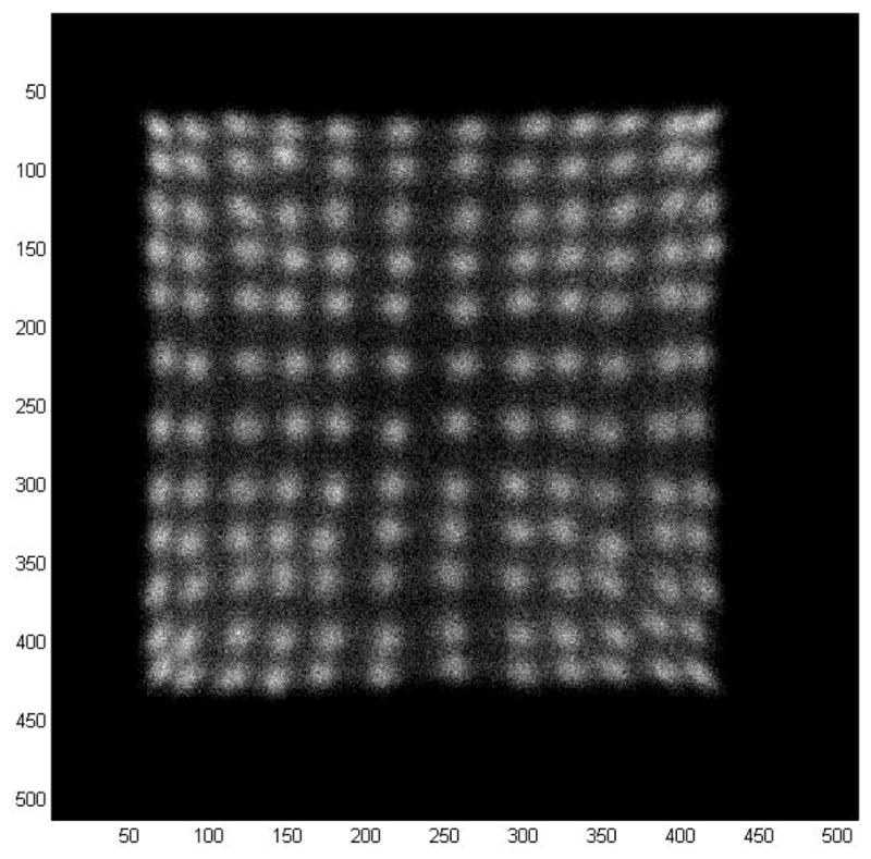
Flood Map from a PET Block Detector Module. The detector module is a 12×12 array of 4×4×22 mm3 LSO crystals. All 144 crystals are clearly resolved, and the energy resolution for individual crystals is between 10% and 12% fwhm with 511 keV excitation.
The maximum singles event rate was 4,565 256-bit events per second, which corresponds to 36,520 32-bit events per second. This rate is two orders of magnitude lower than the theoretical maximum output rate of the PB to the host PC (4×10⁶ 32-bit events per second), and is limited by the USB II driver code presently used in the host PC. With more sophisticated driver software, the transfer rate from the PB to the host PC should be closer to the theoretical maximum rate, which is set by the USB II interface hardware (QuickUSB by Bitwise Systems).
B. Readout of an SiPM Array
The purpose of these electronics is to support as large a variety of detector module designs as possible, so the other module tested was chosen to be as different as possible from a block detector. We therefore constructed a 16×16 array of 3 mm square silicon photomultiplier (SiPM) elements. This array was connected to an interface board that used op-amps to turn this matrix of 256 pixels in to 16 row sum signals and 16 column sum signals. The row sums were then sent to one DB and the column sums to another. Events were read out when one of the row elements was in time coincidence with one of the column elements, and the identities and signal amplitudes of the row and column elements were read out. Each time an event was recorded, the data were displayed by incrementing the pixel at the row / column intersection by the amplitude of that event. Figure 5 shows this display when a 3 mm square by 20 mm long crystal of LSO is placed on one pixel and a 3 mm square by 10 mm long crystal of LSO is placed on another pixel. No external source was used—only the internal 176Lu activity excited the crystals. Figure 5 shows the correct pixels lighting up, with the intensity (correctly) being proportional to crystal volume.
Figure 5.
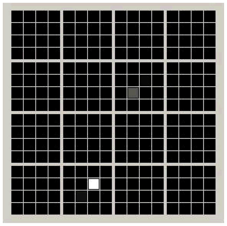
Readout of SiPM Array. A 16×16 array of 3 mm square SiPM elements is read out using a row and column scheme. LSO crystals of different lengths are placed over two of the pixels. The intensity of each pixel in the display is proportional to the event rate in that pixel times the average energy deposited per event. As expected, all but two of the pixels are black, and the pixel with the larger crystal is brighter.
C. Time Digitizer
The final test was of the time to digital converter (TDC) performance. A 16-channel TDC was implemented in an Altera Cyclone II FPGA, as described in [17, 18], and its performance compared to the HPTDC (high performance TDC) developed by CERN [19]. The devices were first tested with a digital input pulse that was sent into two different inputs and the digitized time difference between the two channels recorded. This represents the intrinsic timing resolution of the TDC. With these inputs, the resolution of the HPTDC was 56±6 ps fwhm and the FPGA-based TDC was 90±7 ps fwhm. We then generated timing pulses with a pair of detectors with excellent timing resolution (a Hamamatsu R-9800 PMT coupled to a 6×25 mm2 face of a 6×6×25 mm3 LSO crystal) read out with a Canberra 454 constant fraction discriminator (delay of 0.7 ns, fraction of 0.2) and excited by coincident 511 keV gamma rays from a 200μCi 68Ge source. With these inputs, we measured 268±15 ps fwhm with the HPTDC and 255±13 ps fwhm with the FPGA-based TDC. These values agree with that obtained with NIM-based TDC electronics (258±13 ps fwhm with a Ortec 556 time to amplitude converter and National Instruments PXI-7831R 16-bit analog to digital converter) [20], indicating that the measurement is limited by the detectors and not the TDCs used. Thus, the timing accuracy of these electronics are of high enough quality even for high-performance time-of-flight PET systems. This TDC design is a “locked” portion of the FPGA design file, implying that user modifications to the other logic being performed in the FPGA will not conflict with or affect the TDC performance.
V. Discussion & Conclusions
We have developed a design for a high-performance yet flexible electronics system for radionuclide imaging (notably PET and SPECT) that is targeted to support prototype camera development. One of the most important design considerations was flexibility—that it be able to accommodate as many detector and camera configurations as possible. To achieve this, we maximized the use of programmable logic and minimized the use of analog circuitry. The design features completely independent readout (i.e., energy and timing measurement) of each analog input and the use of a leading edge discriminator (potentially with amplitude correction for time walk) and an FPGA-based TDC to generate an accurate timing signal. FPGAs are extensively used, so the interaction position and time can be computed using data from virtually any combination of analog input channels. Tests with prototype circuit boards excited by test pulses yield 0.1% fwhm energy resolution and 90±7 ps fwhm timing resolution. This suggests that these electronics will not limit the camera performance, and further tests with PET detector modules based on both conventional block detector (4 PMTs decoding 144 crystals with Anger logic) and a SiPM-based detector (256 pixels read out with a row and column architecture) support this assumption.
However, the most novel aspect is probably not technical but sociological. The goal is to create a user community that, by working on a common hardware and software platform, can share the effort necessary to develop electronics for radionuclide imaging systems and so develop systems that are both individually customized and far higher performance than solo development efforts would be. More details are available at http://OpenPET.LBL.gov/ .
Acknowledgments
This work was supported in part by the U.S. Department of Energy under contract No. DE-AC02-05CH11231, and in part by the National Institutes of Health, National Institute of Biomedical Imaging and Bioengineering under grants No. R01-EB006085 and R21-EB007081.
This work is supported in part by the Director, Office of Science, Office of Biological and Environmental Research, Medical Science Division of the U.S. Department of Energy under Contract No. DE-AC02-05CH11231, and in part by the National Institutes of Health, National Institute of Biomedical Imaging and Bioengineering under grants No. R01-EB006085 and R21-EB007081.
Contributor Information
W. W. Moses, Lawrence Berkeley National Laboratory, Berkeley, CA 94720 USA.
S. Buckley, SensL, Cork, Ireland
C. Vu, Lawrence Berkeley National Laboratory, Berkeley, CA 94720 USA
Q. Peng, Lawrence Berkeley National Laboratory, Berkeley, CA 94720 USA
N. Pavlov, SensL, Cork, Ireland
W.-S. Choong, Lawrence Berkeley National Laboratory, Berkeley, CA 94720 USA.
J. Wu, Fermi National Accelerator Laboratory, Batavia, IL 60510 USA
C. Jackson, SensL, Cork, Ireland
VII. REFERENCES
- 1.Young JW, Moyers JC, Lenox M. FPGA based front end electronics for a high resolution PET scanner. IEEE Trans Nucl Sci. 1999;NS-47:1676–1680. [Google Scholar]
- 2.Swann BK, Rochelle JM, Binkley DM, Puckett BS, Blalock BJ, et al. A custom mixed-signal CMOS integrated circuit for high performance PET tomograph front-end applications. IEEE Trans Nucl Sci. 2003;NS-50:909–914. [Google Scholar]
- 3.Wong WH, Hu G, Zhang N, Uribe J, Wang J, et al. Front end electronics for a variable field PET camera using the PMT-quadrant-sharing detector array design. IEEE Trans Nucl Sci. 1997;NS-44:1291–1296. [Google Scholar]
- 4.Moses WW, Young JW, Baker K, Jones W, Lenox M, et al. The electronics system for the LBNL positron emission mammography (PEM) camera. IEEE Trans Nucl Sci. 2001;NS-48:632–636. [Google Scholar]
- 5.Lewellen TK, Miyaoka RS, Janes M, Park B, Gillispie SG, et al. System electronics for the MiCES small animal PET scanner. In: Metzler S, editor. Proceedings of The IEEE Nuclear Science Symposium Conference Record. Portland, OR: 2003. pp. 1770–1774. [Google Scholar]
- 6.Pratte JF, De Geronimo G, Junnarkar S, O'Connor P, Yu B, et al. Front-end electronics for the RatCAP mobile animal PET scanner. IEEE Trans Nucl Sci. 2004;NS-51:1318–1323. [Google Scholar]
- 7.Riendeau J, Berard P, Viscogliosi N, Tetrault MA, Lemieux F, et al. High Rate Photon Counting CT Using Parallel Digital PET Electronics. IEEE Trans Nucl Sci. 2008;NS-55:40–47. [Google Scholar]
- 8.Chaudhari AJ, Yang Y, Farrell R, Dokhale PA, Shah KS, et al. PSPMT/APD hybrid DOI detectors for the PET component of a dedicated breast PET/CT system—A feasibility study. IEEE Trans Nucl Sci. 2008;NS-55:853–861. [Google Scholar]
- 9.Szczesniak T, Moszynski M, Nassalski A, Lavoute P, Dehaine AG. A further study of timing with LSO on XP20D0 for TOF PET. IEEE Trans Nucl Sci. 2007;NS-54:1464–1473. [Google Scholar]
- 10.Haselman MD, Hauck S, Lewellen TK, Miyaoka RS. Simulation of algorithms for pulse timing in FPGAs. In: Yu B, editor. Proceedings of The Nuclear Science Symposium Conference Record. Honolulu, HI: 2007. pp. 3161–3165. [DOI] [PMC free article] [PubMed] [Google Scholar]
- 11.Genat JF, Varner G, Tang F, Frisch H. Signal processing for picosecond resolution timing measurements. Nucl Instr Meth. 2009;A-607:387–393. [Google Scholar]
- 12.Choong WS. The timing resolution of scintillation-detector systems: Monte Carlo analysis. Phys Med Biol. 2009;54 doi: 10.1088/0031-9155/54/21/004. [DOI] [PMC free article] [PubMed] [Google Scholar]
- 13.Ambrosi G, Azzarello P, Battiston R, Di Lorenzo G, Ionica M, et al. Time resolving characteristics of HPK and FBK silicon photomultipliers for TOF and PET applications. Nucl Instr Meth. 2010;A-617:242–243. [Google Scholar]
- 14.Ullisch MG, Moses WW. Multi-CFD timing estimators for PET block detectors. IEEE Trans Nucl Sci. 2007;NS-54:55–59. [Google Scholar]
- 15.Altera Corporation. http://www.altera.com/
- 16.National Instruments. http://www.ni.com/
- 17.Wu J, Shi Z. The 10-ps wave union TDC: Improving FPGA TDC resolution beyond its cell delay. In: Sellin P, editor. Proceedings of The IEEE Nuclear Science Symposium Conference Record. Dresden, Germany: 2008. pp. 3440–3446. [Google Scholar]
- 18.Wu J. An FPGA TDC for time-of-flight applications. In: Yu B, editor. Proceedings of The IEEE Nuclear Science Symposium Conference Record. Orlando, FL: 2009. pp. 299–304. [Google Scholar]
- 19.Akindinov AV, Alici A, Anselmo F, Antonioli P, Basile M, et al. Design aspects and prototype test of a very precise TDC system implemented for the Multigap RPC of the ALICE-TOF. Nucl Instr Meth. 2004;A-533:178–182. [Google Scholar]
- 20.Moses WW, Janecek M, Spurrier MA, Szuprycznski P, Choong WS, et al. Optimization of a LSO-based detector module for time-of-flight PET. IEEE Trans Nucl Sci. 2010;NS-57:1570–1576. doi: 10.1109/TNS.2010.2047266. [DOI] [PMC free article] [PubMed] [Google Scholar]