Flexible nanolithographic and printing methods are essential tools in the field of nanoscience and nanotechnology.[1–5] Scanning probe techniques such as dip-pen nanolithography (DPN)[3, 6–12] and nanografting[13, 14] are extremely useful since they allow one to make nanostructures from a wide variety of different chemical compositions. In the case of DPN, despite significant advances in parallelization,[2,15–17] it is still challenged for certain applications with regard to throughput, especially when compared to lower resolution contact printing methods. Indeed, microcontact printing (μCP) has emerged as a “bench-top” technique for preparing patterns of various active structures in a massively parallel manner.[18–20] In conventional μCP, a soft elastomer stamp (typically polydimethylsiloxane, PDMS) with relief structures predefined by photo- or e-beam lithography is brought into contact with a substrate, where the ink is transferred from the stamp to the substrate surface at the area of contact. [21] PDMS has a Young’s Modulus of ~1 MPa, which is soft enough to make conformal contact with planar or nonplanar surfaces to facilitate ink transfer. However, since the relief structures are separated by air voids in the stamp, the mechanical instability (pairing, sagging, etc.) of the stamp deriving from the “soft” nature of PDMS, has been a major limitation for a variety of applications in μCP.[5, 22, 23] The volatility of the inks and their diffusion properties on a surface also can be limiting factors when printing small features (Scheme 1).[24] Although many solutions have been suggested to address both mechanical and ink-transport issues, such as using harder elastomers[25, 26] and establishing control over printing time, [27] the lateral resolution of printed features and the design of such stamps are still limited to ~150 nm (in terms of alkanethiols) and a ~1/20 filling factor, respectively.[23, 28]
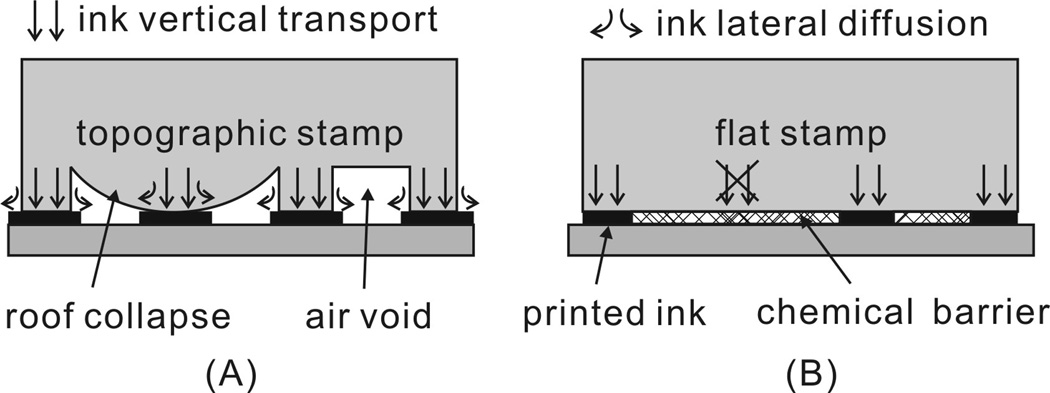
Scheme 1.
Schematic illustration of ink transport during μCP using : (a) a conventional topographic stamp and (b) a chemically patterned flat stamp. Topographic stamps may deform when two relief features (the raised areas of the stamp) are too far away from one another. Ink lateral diffusion also limits the resolution in μCP. In contrast, a chemically patterned flat stamp is mechanically stable. The chemical barrier confines ink vertical transport and prevents ink lateral diffusion.
Herein, we report how one can use DPN to prepare a stamp for high resolution μCP in a way that keeps the PDMS surface topographically flat but chemically patterned. The mechanically stable flat stamp is prepared without a photomask (since the structure may be directly written onto the surface by DPN), and the pattern drawn by DPN combined with subsequent chemical modification of the exposed areas of the stamp, allows one to create a surface with well-defined chemical regions that can be used to confine ink transport to sub-100 nm dimensions and prevent the lateral diffusion of the ink (Scheme 1). Others have used contact inking,[29,30] metal contact masks,[31,32] and template-mediated self-assembly approaches[33] to fabricate (sub)micron-sized chemical patterns on PDMS, but the approach described herein is remarkably simple and straightforward to implement and does not require complex and expensive photo- or e-beam lithography. More importantly, the high registration and resolution of DPN allow one to create stamps using this approach that reproducibly yield sub-100 nm features with an extremely low filling factor (less than 1/100). Herein, we show that with different patterned stamps, one can efficiently generate nano- and microscale structures with alkanethiols, proteins, and water-soluble dyes.
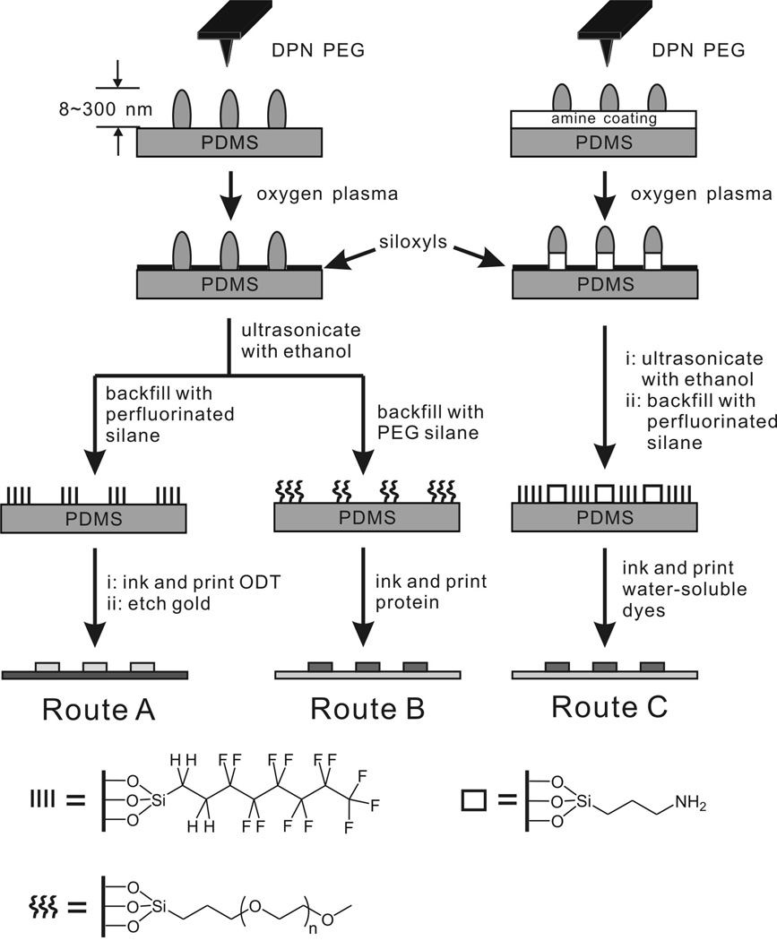
In a typical experiment, polyethylene glycol (PEG) features (80 nm to many μm) were first deposited onto hydrophobic or amine-modified flat PDMS by DPN (Scheme 2). A cantilever array with 12 tips (M-12, NanoInk, Inc.) was dipped into a 5 mg/ml acetonitrile solution of PEG (MW 2,000) for 10 sec, and then dried under flowing N2. The array was then mounted on an NSCRIPTOR™ and used to generate nano- and micron-sized features on PDMS. The writing environment was controlled at 21±1 °C and 92±2% humidity. The PEG thin layer forms a contact mask, which can be used as a chemical resist. Upon treatment with oxygen plasma (200 mTorr, 30 sec), the PDMS surface was selectively rendered hydrophilic, creating siloxyl-rich surfaces on the unmasked areas. After rinsing off the physisorbed PEG by sonication in a water/ethanol (1:1 v/v) bath for 2 min, the siloxyl groups were further reacted with functional silane molecules by a condensation reaction in the gas or liquid phase (vide infra). Finally, the μCP capabilities of chemically patterned flat stamps were studied with the different inks.
Scheme 2.
Schematic illustration of the fabrication of flat stamps for μCP of alkanethiols (route A), proteins (route B) or hydrophilic dyes (route C) by DPN.
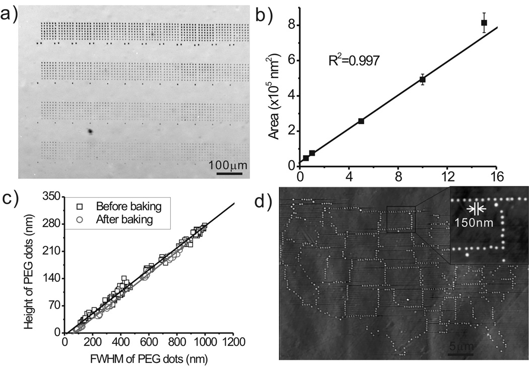
To determine the possibility of using DPN to control the stamp feature size and composition in the context of a flat stamp, we prepared 6×7 arrays of PEG features on PDMS (Figure 1a). Feature size was decreased by decreasing tip-substrate contact time. For example, 15 s resulted in 1.1 μm diameter features (Figure 1a, top row) while 0.1 s gave 140 nm diameter structures (Not shown but confirmed by AFM). As with conventional DPN, [34, 35] the feature size is linearly related to the square root of tip-substrate contact time (Figure 1b), and the diffusion rate under the conditions studied is approximately 4.7×10⁴ nm2/sec. The height of each PEG dot also increases linearly with increasing feature size (Figure 1c). We attribute this behaviour to the hydrophobicity of the PDMS, [36] which keeps the PEG from fully wetting the surface, thereby resulting in a structure with spherical-cap like morphology. This phenomenon ensures that the deposited PEG layer is thick enough to behave as an etch resist even with sub-100 nm features. For instance, we have fabricated PEG stamp features as small as 85±5 nm [full width half maximum (FWHM) of the feature line scan taken by tapping mode AFM], which are 11±1 nm thick (Figure S1, Supporting Information). The 11 nm thick PEG behaves as an excellent resist for the 30 sec oxygen plasma used to prepare the flat stamp. High registration and the ability to tightly control where different micro and nanometer scale features are on a flat stamp are other advantages of depositing PEG by DPN. In this regard, we have shown that one can generate a miniaturized structure consisting of ~2,000 PEG dots in the form of the United States over a 60×40 μm2 area of PDMS. Each dot is approximately 150 nm in diameter, and the distance between neighbouring dots varies from 200 nm to more than 10 μm. The PEG patterned PDMS is typically exposed to an O2 plasma for 30 s followed by rinsing and ultrasonication (to remove the PEG), in order to prepare the areas not blocked with the PEG features for further chemical functionalization. For these experiments, either a perfluorinated silane was used to render those areas ambiphobic[32] or a PEG silane was used to make them resist the adsorption of biomolecules.[31]
Figure 1.
(a) An optical microscope image of PEG patterns generated by DPN with different contact time. Each row was generated by 12 individual pens simultaneously. (b) A plot of the PEG diffusion rate. (c) The height of PEG dots as a function of their FWHM. (d) An AFM topography image of a United States mainland map consisting of ~2,000 PEG nanodots. The inset is a zoom-in image showing that the size of each PEG nanodot is about 150 nm.
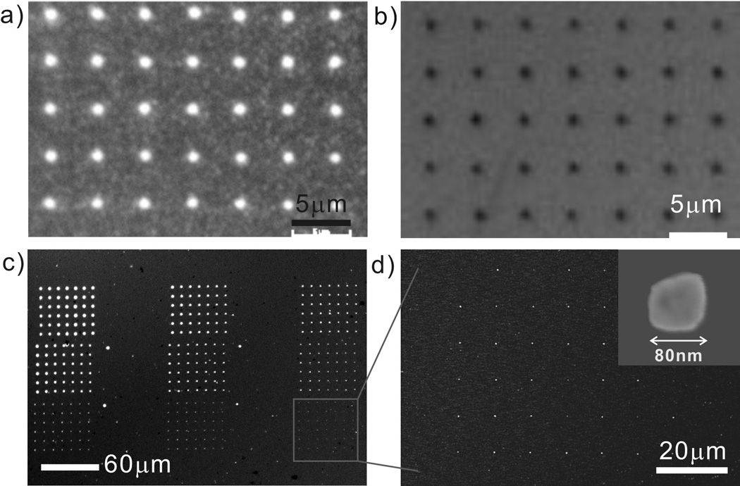
As an initial proof-of-concept, we prepared a flat stamp with a pattern consisting of 7×5 arrays of 1μm dots defined initially by the DPN-generated PEG features with the surrounding areas passivated with 1H,1H,2H,2H-perfluorooctadecyltrichlorosilane (PFODTS). This stamp was immersed in a 2 mM ethanolic solution of octadecanethiol (ODT), rinsed with ethanol, and then blown dry with N2. The ODT goes exclusively to the regions of the stamp not passivated with the PFODTS. When brought in contact with a gold surface, an ODT pattern is generated within 1 min. Removal of the stamp and subsequent etching of the patterned substrate with a gold etching solution yields raised 1 μm gold dot features that can be observed by optical microscopy (Figure 2a). There is less than a 5% variation in feature diameter, as determined by optical microscopy, and the stamp can be used 10 times without a measurable change (by optical microscopy) in feature size or quality. Higher concentration (10 mM) ink gives similar results. However, when PFODTS is replaced by octadecyltrichlorosilane (OTS), ODT spreading is observed on the OTS areas.
Figure 2.
(a) An optical microscope image of a 7×5 gold array fabricated by μCP of ODT with a chemically patterned flat stamp and wet etching. The PEG mask used for making the flat stamp is shown in (b). (c) A SEM image of 7×6 gold arrays with various sizes from 3.5 μm to sub-100 nm. (d) A zoom-in image of a sub-100 nm-sized gold array in (c). The inset details the size of a gold island.
With the flat stamps made by DPN, one can fabricate gold structures that span the sub-100 nm to many micrometer length scales with controllable feature spacing (Figure 2c, d and Figure S2). For example, we have prepared stamps capable of producing 4 μm diameter features and ~80 nm features with 10 μm periodicity in the same pattern. Note that because of the polycrystalline nature of the gold, the sub-100 nm features often are not perfectly circular. No pinholes are observed (by SEM) in these structures, including the sub-100 nm ones, indicating that the printed ODT forms a closely packed resist layer. The filling factor is less than 0.01 in the sub-100 feature area. To the best of our knowledge, this is the lowest filling factor reported for sub-100 nm gold patterns fabricated by μCP.
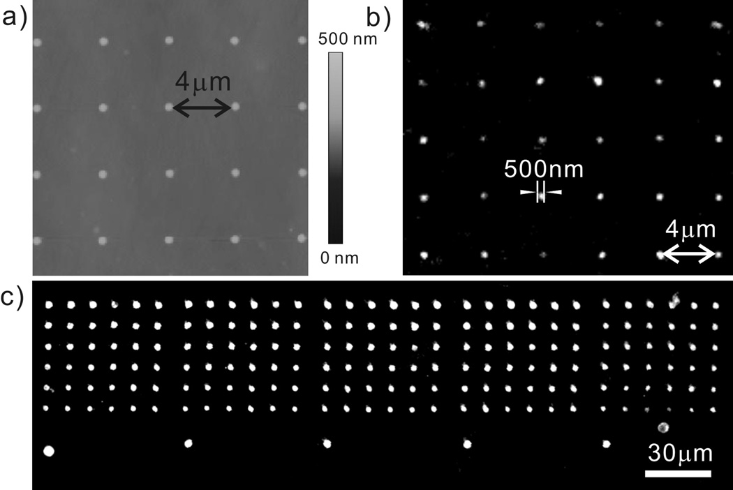
To further probe the versatility of this approach, we fabricated a PDMS flat stamp with 500 nm dot features (defined initially by DPN generated PEG layers, Figure 3a), in which the surrounding areas are passivated with PEG silane, and evaluated its utility for making protein arrays by μCP (Scheme 2, Route B). Proteins often exhibit strong interactions with hydrophobic surfaces such as PDMS, but modification with PEG silane can significantly inhibit protein adsorption.[31] In a typical experiment, we immersed our PEG-silane-passivated flat stamp into a 1 mg/ml tetramethylrhodamine 5-(and-6)-isothiocyanate (TRITC) conjugated anti-mouse IgG solution for 10 min. The stamp was subsequently rinsed with PBS buffer and Mili-Q water to remove protein residue on the PEG passivated areas of the stamp. Finally, the stamp was used to print 500 nm diameter IgG protein features on an ethanol-cleaned glass slide by holding it in contact with the glass substrate for 10 min, Figure 3b. The pattern was characterized by fluorescence microscopy and shows relatively uniform protein feature transfer with the intended 4 μm spacing.
Figure 3.
(a) An AFM topography of the PEG pattern used for fabricating a flat stamp for μCP of proteins. (b) A fluorescent image of the printed TRITC conjugated anti-mouse IgG. (c) A fluorescent image of the printed TRITC pattern on glass.
The intrinsic drawbacks in conventional microcontact printing, i.e. roof collapse and lateral ink diffusion, were addressed by using topographically flat, chemically patterned PDMS stamps made by Dip-Pen Nanolithography (DPN). The chemically patterned flat stamps were used for contact printing of various inks including thiols, proteins and hydrophilic dyes. The as-made features can reach sub-100 nm resolution and very low filling factor (<1/100).##DPN benefits μCP
dip-pen nanolithography
microcontact printing
silanes
nanofabrication
surface chemistry
In conclusion, we have presented a versatile method for fabricating topographically flat, chemically patterned PDMS stamps by DPN. These flat stamps are mechanically stable and the chemical patterns on their surfaces (generated by DPN) allow one to deliberately control where ink transport takes place, on the sub-100 nm to many μm length scale. This novel capability increases the resolution of conventional μCP, allows one to prepare structures with exceedingly low filling factors, and bypasses some of the deformation problems typically associated with conventional relief structure stamps. Importantly, the technique still allows for a wide range of inks, even polar inks (Figure 3c, and see Supporting Information for details), which may prove useful for many researchers, including those in the life sciences.
Experimental Section
Chemicals
Polyethylene glycol (PEG, MW 2,000), octadecanethiol (ODT), 3-aminopropryltriethoxylsilane (APTES), thiourea, iron nitrate, tetramethylrhodamine 5-(and-6)-isothiocyanate (TRITC), TRITC conjugated anti-mouse IgG, and octanol were purchased from Sigma Aldrich (MN, USA). 1H,1H,2H,2H-perfluorooctadecyltrichlorosilane (PFODTS) was purchased from Gelest (PA, USA). PEG-silane (MW 2,000) was purchased from Ropp Polymere (Germany). Sylgard 184 kit was purchased from Dow Corning (MI, USA). All of the chemicals were used without further purification. Au films were etched by aqueous etching solution containing 20 mM thiourea, 30 mM iron nitrate, 20 mM hydrochloric acid, and 2 mM octanol.
PDMS fabrication
Prepolymer Sylgard 184 and its curing agent were mixed in a ratio of 10:1, debubbled, and then cast on a flat plastic petridish. After being cured at 70 °C over night, the PDMS was peeled from the petridish for further modification to prepare the flat stamps.
Silanization
Flat PDMS or PEG patterned PDMS stamps were first exposed to oxygen plasma for 30 sec (200 mTorr). PEG patterned PDMS required additional sonication in a water/ethanol (1:1 v/v) bath for 3 min to remove the physisorbed PEG mask. The stamp was then exposed to a silane vapor or solution for silanization. For reaction with APTES, the stamp was immersed in 1% v/v APTES in ethanol for 1 hr, cured at 90 °C for 30 min, and ultrasonicated in ethanol for 3 min. For reaction with PEG silane, the stamp was immersed in 1 mM PEG silane in aqueous acidic solution (pH=2, adjust with concentrated HCl) for 2 hr, and then rinsed with pure water. For reaction with PFODTS, the stamp was exposed to its vapour in a sealed desiccator under reduced pressure for 30 min, and rinsed with fresh ethanol.
Supplementary Material
Footnotes
C.A.M. acknowledges the AFOSR, DARPA, and NSF for support of this research. C.A.M is also grateful for the NIH Director’s Pioneer Award and a NSSEF Fellowship from the DoD.
References
- 1.Salaita K, Wang Y, Mirkin CA. Nat. Nanotech. 2007;2:145. doi: 10.1038/nnano.2007.39. [DOI] [PubMed] [Google Scholar]
- 2.Mirkin CA. ACS Nano. 2007;1:79. doi: 10.1021/nn700228m. [DOI] [PubMed] [Google Scholar]
- 3.Ginger DS, Zhang H, Mirkin CA. Angew. Chem. Int. Ed. 2004;43:30. doi: 10.1002/anie.200300608. [DOI] [PubMed] [Google Scholar]; Angew. Chem. 2004;116:30. [Google Scholar]
- 4.Gates BD, Xu QB, Stewart M, Ryan D, Willson CG, Whitesides GM. Chem. Rev. 2005;105:1171. doi: 10.1021/cr030076o. [DOI] [PubMed] [Google Scholar]
- 5.Geissler M, Xia Y. Adv. Mater. 2004;16:1249. [Google Scholar]
- 6.Piner RD, Zhu J, Xu F, Hong S, Mirkin CA. Science. 1999;283:661. doi: 10.1126/science.283.5402.661. [DOI] [PubMed] [Google Scholar]
- 7.Lee K-B, Park S-J, Mirkin CA, Smith JC, Mrksich M. Science. 2002;295:1702. doi: 10.1126/science.1067172. [DOI] [PubMed] [Google Scholar]
- 8.Demers LM, Ginger DS, Park SJ, Li Z, Chung SW, Mirkin CA. Science. 2002;296:1836. doi: 10.1126/science.1071480. [DOI] [PubMed] [Google Scholar]
- 9.Zhang H, Elghanian R, Amro NA, Disawal S, Eby R. Nano Lett. 2004;4:1649. [Google Scholar]
- 10.Nyamjav D, Ivanisevic A. Adv. Mater. 2003;15:1805. [Google Scholar]
- 11.Ivanisevic A, Mirkin CA. J. Am. Chem. Soc. 2001;123:7887. doi: 10.1021/ja010671c. [DOI] [PubMed] [Google Scholar]
- 12.Coffey DC, Ginger DS. J. Am. Chem. Soc. 2005;127:4564. doi: 10.1021/ja0428917. [DOI] [PubMed] [Google Scholar]
- 13.Xu S, Miller S, Laibinis PE, Liu Gy. Langmuir. 1999;15:7244. [Google Scholar]
- 14.Amro NA, Xu S, Liu Gy. Langmuir. 2000;16:3006. [Google Scholar]
- 15.Salaita K, Wang Y, Fragala J, Vega RA, Liu C, Mirkin CA. Angew. Chem. Int. Ed. 2006;45:7220. doi: 10.1002/anie.200603142. [DOI] [PubMed] [Google Scholar]; Angew. Chem. 2006;118:7378. [Google Scholar]
- 16.Hong S, Mirkin CA. Science. 2000;288:1808. doi: 10.1126/science.288.5472.1808. [DOI] [PubMed] [Google Scholar]
- 17.Lenhert S, Sun P, Wang Y, Fuchs H, Mirkin CA. Small. 2007;3:71. doi: 10.1002/smll.200600431. [DOI] [PubMed] [Google Scholar]
- 18.Xia Y, Whitesides GM. Angew. Chem. Int. Ed. 1998;37:551. doi: 10.1002/(SICI)1521-3773(19980316)37:5<550::AID-ANIE550>3.0.CO;2-G. [DOI] [PubMed] [Google Scholar]; Angew. Chem. 1998;110:568. [Google Scholar]
- 19.Yousaf MN, Houseman BT, Mrksich M. Proc. Natl. Acad. Sci. 2001;98:5992. doi: 10.1073/pnas.101112898. [DOI] [PMC free article] [PubMed] [Google Scholar]
- 20.Zhou F, Zheng Z, Yu B, Liu W, Huck WTS. J. Am. Chem. Soc. 2006;128:16253. doi: 10.1021/ja0654377. [DOI] [PubMed] [Google Scholar]
- 21.Kumar A, Whitesides GM. Appl. Phys. Lett. 1993;63:2002. [Google Scholar]
- 22.Alexander B, Bruno M. J. Appl. Phys. 2000;88:4310. [Google Scholar]
- 23.Sharp KG, Blackman GS, Glassmaker NJ, Jagota A, Hui CY. Langmuir. 2004;20:6430. doi: 10.1021/la036332+. [DOI] [PubMed] [Google Scholar]
- 24.Libioulle L, Bietsch A, Schmid H, Michel B, Delamarche E. Langmuir. 1999;15:300. [Google Scholar]
- 25.Schmid H, Michel B. Macromolecules. 2000;33:3042. [Google Scholar]
- 26.Odom TW, Love JC, Wolfe DB, Paul KE, Whitesides GM. Langmuir. 2002;18:5314. [Google Scholar]
- 27.Helmuth JA, Schmid H, Stutz R, Stemmer A, Wolf H. J. Am. Chem. Soc. 2006;128:9296. doi: 10.1021/ja062461b. [DOI] [PubMed] [Google Scholar]
- 28.Geissler M, Wolf H, Stutz R, Delamarche E, Grummt UW, Michel B, Bietsch A. Langmuir. 2003;19:6301. [Google Scholar]
- 29.Geissler M, Bernard A, Bietsch A, Schmid H, Michel B, Delamarche E. J. Am. Chem. Soc. 2000;122:6303. [Google Scholar]
- 30.Coyer SR, García AJ, Delamarche E. Angew. Chem. Int. Ed. 2007;46:6837. doi: 10.1002/anie.200700989. [DOI] [PubMed] [Google Scholar]; Angew. Chem. 2007;119:6961. [Google Scholar]
- 31.Delamarche E, Donzel C, Kamounah FS, Wolf H, Geissler M, Stutz R, Schmidt-Winkel P, Michel B, Mathieu HJ, Schaumburg K. Langmuir. 2003;19:8749. [Google Scholar]
- 32.Sharpe RBA, Burdinski D, Huskens J, Zandvliet HJW, Reinhoudt DN, Poelsema B. J. Am. Chem. Soc. 2005;127:10344. doi: 10.1021/ja052139l. [DOI] [PubMed] [Google Scholar]
- 33.van Poll ML, Zhou F, Ramstedt M, Hu L, Huck WTS. Angew. Chem. Int. Ed. 2007;46:6634. doi: 10.1002/anie.200702286. [DOI] [PubMed] [Google Scholar]; Angew. Chem. 2007;119:6754. [Google Scholar]
- 34.Weinberger DA, Hong S, Mirkin CA, Wessels BW, Higgins TB. Adv. Mater. 2002;14:231. [Google Scholar]
- 35.Weeks BL, Noy A, Miller AE, De Yoreo JJ. Phys. Rev. Lett. 2002;88:255505. doi: 10.1103/PhysRevLett.88.255505. [DOI] [PubMed] [Google Scholar]
- 36.Zheng Z, Azzaroni O, Zhou F, Huck WTS. J. Am. Chem. Soc. 2006;128:7730. doi: 10.1021/ja061636e. [DOI] [PubMed] [Google Scholar]
- 37.Duan X, Sadhu VB, Perl A, Péter M, Reinhoudt DN, Huskens J. Langmuir. 2008;24:3621. doi: 10.1021/la702975q. [DOI] [PubMed] [Google Scholar]
Associated Data
This section collects any data citations, data availability statements, or supplementary materials included in this article.


