Abstract
A simple, versatile approach to the directed self-assembly of block copolymers into a macroscopic array of unidirectionally aligned cylindrical microdomains on reconstructed faceted single crystal surfaces or on flexible, inexpensive polymeric replicas was discovered. High fidelity transfer of the line pattern generated from the microdomains to a master mold is also shown. A single-grained line patterns over arbitrarily large surface areas without the use of top-down techniques is demonstrated, which has an order parameter typically in excess of 0.97 and a slope error of 1.1 deg. This degree of perfection, produced in a short time period, has yet to be achieved by any other methods. The exceptional alignment arises from entropic penalties of chain packing in the facets coupled with the bending modulus of the cylindrical microdomains. This is shown, theoretically, to be the lowest energy state. The atomic crystalline ordering of the substrate is transferred, over multiple length scales, to the block copolymer microdomains, opening avenues to large-scale roll-to-roll type and nanoimprint processing of perfectly patterned surfaces and as templates and scaffolds for magnetic storage media, polarizing devices, and nanowire arrays.
Keywords: block copolymer, directed self-assembly, long-range order, pattern transfer
With the ever-diminishing size scale of device elements, the directed self-assembly (DSA) of block copolymers (BCPs), a highly parallel process, offers a simple, robust route for generating nanostructured materials that overcomes the technological and economic limitations associated with large-scale “top-down” lithographic approaches (1, 2). The use of DSA in nanotechnology requires strategies to achieve control over large areas in an efficient, cost-effective manner that is compatible with high precision industrial processes.
The grand challenge of generating addressable, macroscopic arrays of nanoscopic elements where the spatial position of each element is precisely known by the DSA of BCPs remains. Chemical and topographic patterning have been used for the DSA of BCPs, but this has been restricted to areas < 1 mm2 due to the significant time and cost to achieve this over macroscopic areas and with long-range translational order (3, 4–13). Producing unidirectionally aligned nanoscopic line patterns, though the simplest of patterns and a key element for semiconductor, magnetic, and optical devices (3, 14), has still yet to be achieved by the DSA of BCPs. Interferometric lithography has been investigated to produce sub-50 nm pitch line patterns, but this also encounters similar impediments (15). Zone annealing and shearing can be used to affect nanoscopic line patterns over areas > 1 mm2, but shearing is limited by the thickness of the films required and both processes generate patterns containing numerous defects (16, 17).
Here, we show that unidirectionally aligned, nanoscopic line patterns can be produced over arbitrarily macroscopic areas using the surface topography of reconstructed sapphire or replicas on flexible polymer substrates by the DSA of BCPs in a thermodynamically robust manner. Even though these surfaces contain numerous defects, like dislocations and a distribution of the pitch between the ridges, unidirectional alignment can be achieved where the short and long wavelength waviness, inherent to the BCP microdomains, are suppressed and unidirectionally aligned line patterns, with an order parameter in excess of 0.97, can be produced over the entire surface. The alignment of the cylindrical microdomains is driven by the entropy of chain packing and, as such, represents the free energy minimum of the system.
Results and Discussion
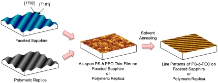
Fig. 1 shows the route to produce line patterns in thin films of polystyrene-block-poly(ethylene oxide) copolymer (PS-b-PEO) on a faceted sapphire surface and an imprinted polymeric replica. A thin film of cylinder-forming PS-b-PEO (Mn = 26.5 kg/mol) that, in the bulk, orders into hexagonal arrays of cylindrical microdomains with a center-to-center distance of L2 = L1 × (2/√3) = 32.5 nm in bulk (the domain spacing of hexagonally packed cylindrical microdomains is L1 = 2π/q∗ = 28.2 nm) was spin coated onto a faceted sapphire surface or an imprinted polymer replica and then exposed to tetrahydrofuran (THF), a good solvent for both blocks, and water, a good solvent for only the PEO block, to produce a well-developed nanostructure.
Fig. 1.
Schematic illustrations of preparation of highly ordered and oriented line pattern of block copolymer thin films on a faceted sapphire and on an imprinted polymeric replica. PS-b-PEO (Mn = 26.5 kg/mol) thin films are prepared onto these faceted substrates and solvent annealed with THF and water.
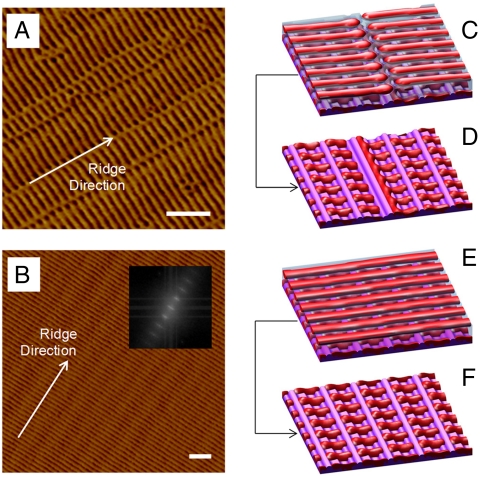
Figs. 2A and 2B show scanning force microscopy (SFM) images of solvent-annealed PS-b-PEO thin films under different annealing conditions. When a PS-b-PEO thin film with a thickness of 38.0 nm (as measured on a flat substrate) is solvent-annealed for 0.5 h, hexagonally packed PEO microdomains, oriented normal to the film surface result with long-range lateral order (see Fig. S1B). With increased annealing time the PEO microdomains fuse to form cylindrical microdomains oriented parallel to the film surface but orthogonal to the facet ridges (see Fig. S1 A and C). The cylindrical microdomains are truncated at the crests of the facets (Fig. 2A and see Fig. S2), since the amplitudes of the facets are comparable to the initial film thickness. These truncated cylindrical microdomains are seen regardless of the distance between the crests of the facets and, as will be discussed, are essential in achieving a high order parameter. By increasing the thickness of the film to 47.5 nm (as measured on a flat substrate), the microdomains span across the facets (see Figs. S1D and S3) forming unidirectionally aligned PEO cylindrical microdomains oriented parallel to the surface and orthogonal to the facets (Fig. 2B). Since the thickness of this film is less than 2 L1, a monolayer of cylindrical microdomains was produced. The Fourier transform (shown in Inset) shows multiple higher-order interferences, characteristic of the long-range lateral ordering of the cylindrical microdomains. Micrographs identical to that in Fig. 2B were obtained over the entire surface showing that the ordering was preserved. Identical results were obtained for other BCPs like polystyrene-block-poly(2-vinylpyridine) copolymer (PS-b-P2VP) (see Fig. S4A), underscoring the generality of our strategy.
Fig. 2.
SFM phase images of PS-b-PEO (Mn = 26.5 kg/mol) thin films on the faceted sapphire substrate, where the film thicknesses are 38.0 nm for (A) and 47.6 nm for (B) and the solvent annealing times are 2 h. The Inset in Fig. 2B is the Fourier transform of SFM image of Fig. 2B. The scale bars are 200 nm. Cahn-Hilliard-Cook and Landau-Ginzburg simulated morphologies of cylinder-forming AB diblock copolymer films with a thickness of (C), Δ = 1.0 L1 and (E), Δ = 1.1 L1 on the faceted pattern having a pitch size of λ = 1.7 L1, where L1 is a domain spacing of cylindrical microdomains, 2π/q∗. Regions of high density of A and B block are colored opaque maroon and translucent blue, respectively, and the saw-toothed substrate is represented by purple color. The morphologies in (D) and (F) are the lower half of the films of (C) and (E), respectively.
Insight into the DSA of BCPs on the faceted surfaces was obtained from density functional theory simulations for cylinder-forming BCPs on neutral faceted surfaces. Results of the simulations for different films thicknesses are shown in Fig. 2 C–F (details provided in SI Text). As can be seen, the similarities between the calculations and the experiments are striking. An important aspect of the assembly of the cylindrical microdomains is that, immediately adjacent to the substrate, truncated cylindrical microdomains form between the apices of the facets (highlighted in Figs. 2D and 2F) that guide the first complete layer of cylindrical microdomains spanning the ridges (Figs. 2C and 2E). These highly oriented microdomains are observed regardless of the separation distance between adjacent apices guiding the next layer of cylindrical microdomains and, coupled with the bending modulus of the cylindrical microdomains, produce exceptionally straight cylindrical microdomains. The short and long wavelength waviness was characterized by determining the local tangents of the microdomains and their deviation away from the overall axes of the microdomains. This we term the slope error (see Figs. S5 and S6). For the cylindrical microdomains oriented normal to the facet ridges, a slope error of 1.1° was found. Analysis of previously published results on well-aligned cylindrical microdomains confined within a trench over very limited areas yields, at best, a slope-error value of 1.5°, with more typical values of 3° being found (18–21): it is noted that we analyzed these data based on the reported figures in the published papers. Consequently, for the cylindrical microdomains self-assembling on faceted surfaces, the entropic penalties associated with chain packing and the incommensurability between the pitch of the facets and period of the BCP, result in an orientation of the microdomains normal to the facets.
The free energies of cylindrical microdomains oriented normal (F+) and parallel to the facets (F||), in the strong segregation limit (22), are the sum of three terms: F = Fst + FAB + FS, where Fst is the stretching energy of AB block copolymer, FAB the A/B interfacial energy, and FS is the surface/polymer interfacial energy. Fst is given by
 |
where Fb is the bulk free energy of the cylindrical microdomain morphology, f is the volume fraction of the minority block (A block), V is the volume of the film, ∫Vαdr indicates an integral over the volume of the α-domain (α = A or B), and z is the shortest distance from the A/B interface. FAB and FS are given by:
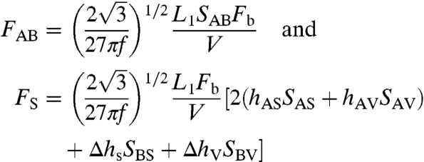 |
where Sαβ is the α/β interfacial area (the subscripts S and V denote the substrate and vapor, respectively), hαβ = γαβ/γAB and Δhα = (γBα - γAα)/γAB with α/β interfacial tension γαβ. Here, we consider the case ΔhS > 0 and ΔhV = 0, i.e., the substrate preferentially interacts with the minority A block (ΔhS = 0.1) whereas the solvent vapor at the film surface is energetically neutral for both blocks.
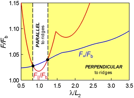
For a BCP film on a faceted surface with two facet angles (θ1 = 17.6°, θ2 = 32.4°), the free energy per chain (in units of bulk free energy) was calculated (Fig. 3) as a function of λ (in units of L2) when the substrate is selective for the A block and Δ = 1.1L1. When λ/L2 < 1.5, orienting the cylindrical microdomain parallel to the ridges is favored. F|| is a minimum, as would be expected, when λ/L2 = 1.0. When λ/L2 > 1.5, F|| shows another minimum at λ/L2 ≅ 1.7. The noninteger value arises from the elastic penalty due to the diagonal confinement of the microdomain lattice by the faceted surface. F+ is less dependent on λ/L2, since the cylindrical microdomains can relieve the packing frustration by orienting the cylinders across the valley of the facet, where the film thickness is maximum. If F+ < F||, orientation of the cylindrical microdomains normal to the ridges is thermodynamically favored. When λ/L2 is small (λ/L2 < 0.84), incommensurability between λ with L2 forces the microdomains to orient normal to the ridges and when λ/L2 > 1.2, (applicable to our study) perturbations to the lattice by large corrugations (in amplitude and pitch) cause the orthogonal orientation to be more favored irrespective of pitch. Since there is a distribution of pitches on the faceted surface and λ/L2 > 1.23 for all the pitches, the orientation of the cylindrical microdomains is insensitive to the pitch of the facets (see Fig. 2B), identical to the experimental results in Figs. 2A and 2B. If a solvent is used that is selective for the major component, orientation of the microdomains normal to the surface, as seen in our previous studies (23), is favored.
Fig. 3.
The free energies per chain of cylinders parallel to the facets (red line: F||) and orthogonal to the facets (blue line: F+) as a function of pitch for the BCP films with {f = 0.25, Δ/L1 = 1.1, θ1 = 17.6°, θ2 = 32.4°, hAS = 0.0, ΔhS = 0.1, hAV = 0.0, ΔhV = 0.0.}. The free energy and the pitch are normalized by bulk free energy and L2 at bulk, respectively. The black filled circles represent the transition point between two different cylinder orientations.
Pickett et al. considered the orientation of lamellar microdomains on a sinusoidally rippled substrate (24), while Kim et al. (3) investigated substrates lithographically patterned with trenches where the interfacial interactions were balanced. In both cases, the lamellar microdomains oriented normal to the pattern. Frustration effects near the boundary of the trenches, which are regions of high stress for chains oriented parallel to the trench walls, were argued to be responsible for the BCP orientation. The orientation of BCP cylindrical microdomains was also controlled by graphoepitaxy, where the lithographically patterned trenches guided the self-assembly of the BCPs parallel to the confining walls (25). In our studies on cylinder-forming BCPs on faceted substrates, where the minor component interacts preferentially with the substrate, the origin of the orientation of the microdomains is fundamentally different. The triangular grooves, characteristic of the faceted substrate, impose severe packing constraints on the BCP chains which lead to the orientation of the microdomains normal to the facets.
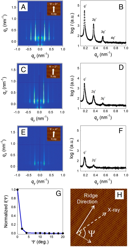
Experimentally, the orientation and grain size of the BCP microdomains can be characterized using Voronoi diagrams and Moiré patterns derived from SFM images (26, 27), but only the local ordering over areas < 20 × 20 μm2. Grazing incidence small angle X-ray scattering (GI-SAXS) was used to assess the lateral ordering and orientation of the microdomains from the nanoscopic to macroscopic length scales (23, 28). Fig. 4 shows the GI-SAXS patterns of a PS-b-PEO thin film corresponding to the sample in Fig. 2B. The incident angle was fixed at 0.18°, which is above the critical angle of the BCP, so that the X-ray beam penetrates the polymer film and the projection of the X-ray beam onto the surface is > 0.100 × 1.00 cm2. By orienting the incident X-ray beam, Bragg rods are observed at scattering vectors with magnitudes of n(L2/2π), where n is an integer, as shown in Figs. 4A and 4B. No scattering from the facets was observed, so that the ridge and cylindrical microdomains direction are not the same and, as discussed later, are orthogonal, in agreement with theory and simulations. The beam stop occluded the specularly reflected beam (see Fig. S7 for the GI-SAXS pattern when the ridges of the facets are parallel to the direction of the X-ray beam). From these data, L2 = 34.9 nm, the same as seen in the bulk. When the sample is rotated by only 2° (Fig. 4C), the (1 0) reflections broaden and weaken by an order of magnitude. With another 2° rotation, the intensity decreases by more than two orders of magnitude (Fig. 4E). Fig. 4B shows the 1D profile of Fig. 4A along qy (in the plane of the film) where multiple orders of scattering are seen from this monolayer of highly aligned cylindrical microdomains. The dependence of the scattering on the rotation angle of the sample with respect to the plane of incidence of the X-ray beam (Fig. 3G and 3F) yields an orientation parameter, f, (see SI Text for calculating f in the case of 2D objects in a thin film) where, for perfect orientation of the microdomains, f = 1.0 and, for random orientation, f = 0. Here, f is found to be 0.99, characteristic of single grain of unidirectionally aligned cylindrical microdomains. It is noted that only the size of the single crystalline substrate limits the area over which this line pattern can be achieved.
Fig. 4.
GI-SAXS patterns of PS-b-PEO thin films on the faceted sapphire substrate. (A) The X-ray beam follows the (1 0) lattice line. From this point, the sample stage is rotated to 2° (C) and 4° (E). The line profiles of scattering as a function of the scattering vector in (B), (D), and (F) are corresponding to (A), (C), and (E), respectively. qy is the in-plane scattering vector. (G) Plot of the integrated intensities of the first-order reflection as a function of rotation angle. These data were used to calculate the orientation parameter with respect to the normal of the ridge direction. (H) Schematic representation for defining rotation angle, Ψ.Ψ is defined as the angle between the direction of the X-ray beam and the direction of cylindrical BCP microdomains.
Developing a simple way to generate such highly aligned cylindrical microdomains on substrates that are flexible, inexpensive, and easy to prepare is highly desirable for applications ranging from flexible displays to roll-to-roll processes. Poly(butylene terephthalate) (PBT) was used to replicate the faceted sapphire surface with high fidelity (29). A solution of PS-b-PEO (Mn = 26.5 kg/mol) in benzene was spin-coated onto the PBT replica and solvent annealed with THF and water. The X-ray beam can pass through the PBT, so transmission SAXS was used to characterize the ordering (see Figs. S8 and S9).
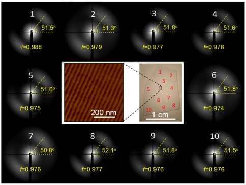
The diffuse scattering arises from the PBT substrate (see Fig. S8) and for a solvent-annealed 47.6 nm thick PS-b-PEO film, reflections are observed (indicated by the arrow in the Fig. S8C,  ) at scattering vectors with magnitudes of n(2L/2π), where n is an integer. First and second order reflections (n = 1 and 2) are evident and, by measuring the scattering for extended times, up to the fifth order reflection (n = 5) can be observed, reflecting the high degree of lateral ordering. The narrow azimuthal angular spread of the reflections are characteristic of a single grain of unidirectionally aligned cylindrical microdomains over the area illuminated by the X-ray beam (1.0 × 0.7 mm2). From the azimuthal-angle dependence of the scattering in Fig. 5 (1–10) (see also Fig. S9), an orientation function of 0.98 ± 0.005 was obtained. By enlarging the area near the beamstop, streaks arising from the facets are observed (indicated by the arrow in the Fig. S8D,
  ) where the direction of the streaks is orthogonal to BCP patterns. This unequivocally shows that the cylindrical microdomains orient normal to the ridges. By translating the sample in the beam, multiple exposures were taken with identical results where, to within the accuracy of the translation, the orientation was preserved, as shown in Fig. 5. These results indicate that the PS-b-PEO film consists of a single grain of unidirectionally aligned cylindrical microdomains oriented parallel to the surface that covers the entire surface.
Fig. 5.
2D Transmission SAXS results of PS-b-PEO thin film on the faceted PBT replica. Ten different areas are randomly selected from the annealed BCP thin film on the replica, which size is over cm2. The director angles where the intensities corresponding to q∗ are maximum and the calculated orientation parameters corresponding to 1 to 10 are indicated.
For large-scale roll-to-roll-type and nanoimprint processing, the unidirectional line pattern must be transferable. Using a line pattern from PS-b-P2VP on the faceted sapphire substrate, the films were exposed to ethanol, a preferential solvent for P2VP that swelled the P2VP microdomains. Removal of the ethanol resulted in reduction of the density of the cylindrical microdomains. Reactive ion etching produced a block copolymer film with trenches having a center-to-center distance of L2. This trench pattern served as a master. A thick film of siloxane precursor was coated onto the master where, by thermal annealing, capillary force drew the siloxane precursor into the trenches. Subsequently, the siloxane precursor was crosslinked, forming a flexible, crosslinked siloxane master. After peeling the crosslinked siloxane mold from the template, a unidirectionally aligned line pattern was transferred with high fidelity (see Fig. S4B). This master mold can then be used as a secondary master for subsequent pattern transfer to the surface of virtually any polymer.
In summary, we have demonstrated a simple route to produce unidirectionally aligned line patterns from the DSA of BCPs on both hard and soft faceted substrates over arbitrarily large areas. The short and long wavelength waviness, inherent to cylindrical BCP microdomains in the bulk, were suppressed in a thermodynamically robust manner. A high fidelity pattern transfer to an imprint mold, i.e., a secondary master, was demonstrated. These films are ideal platforms for the fabrication of magnetic storage media, polarizing devices, and arrays of nanowires.
Materials and Methods
Polystyrene-block-poly(ethylene oxide) copolymer (PS-b-PEO) (20 Kg∕mol for PS and 6.5 kg∕mol for PEO) and polystyrene-block-poly(2-vinylpyridine) copolymer (PS-b-P2VP) (40 Kg∕mol for PS and 18 kg∕mol for P2VP) were purchased from Polymer Source Inc. and used as received. The facets are produced by thermally annealing a single crystal surface of sapphire, cut along the M-plane (a crystallographic plane that is unstable at elevated temperatures), at 1500 °C for 24 h in air (30, 31). The surface reconstructs to form stable crystal facets, resulting in a saw-toothed topography over the entire surface, where the orientation of the facets is in register with the underlying single crystal. Thin films of block copolymers (BCPs) were prepared by spin-coating solutions of PS-b-PEO and benzene onto the substrates where the film thickness was controlled by adjusting the concentration of solution and the speed of spin coating. Solvent annealing was performed in THF and water vapor environment. A preswelling of the BCP film in water vapor was performed to prevent dewetting during the solvent annealing. This was followed by a solvent annealing in THF and water vapor to generate well-developed nanostructures. The poly(dimethylsiloxane) elastomer used in this work was prepared from Sylgard 184 (Dow Corning Corp.). A liquid prepolymer and curing agent were mixed together and the mixture was allowed to cure onto BCP template. Grazing incidence small angle X-ray scattering (GI-SAXS) measurements were performed on the beamline 7.3.3 at the Advanced Light Source in the Lawrence Berkeley National Laboratory. The X-ray beam was delivered onto the sample at an angle above the critical angle of the polymer film (αc = 0.16) but below the critical angle of the planar sapphire substrate (αc = 0.28) (see Supporting Information for the effect of roughness of the faceted substrate on GI-SAXS measurements). 2D transmission X-ray scattering measurements were also performed on the beamline 7.3.3 at the Advanced Light Source at the Lawrence Berkeley National Laboratory. The wavelength of X-rays used was 1.23984 Å, and the scattered intensity was detected by using 2D charge-coupled device (CCD) camera having 2304 × 2304 pixels.
Supplementary Material
ACKNOWLEDGMENTS.
The authors gratefully acknowledge C. Wang at the Advanced Light Source, Berkeley National Laboratory for his assistance with the slope-error analysis. This work was supported by the U.S. Department of Energy (DOE), Office of Basic Energy Sciences (T.P.R., S.W.H., X.G.), the NSF supported Materials Research Science and Engineering Center (D.H.L.) and the NSF-supported Center for Hierarchical Manufacturing (D.H.L.) at the University of Massachusetts Amherst and the Office of Naval Research Young Investigator Program (T.X.). This work was also supported by the Korea Science and Engineering Foundation (KOSEF, No. 2009-0083869) grant funded by the Korean government (MEST) (J.H.). This work was also supported by the Korea Science and Engineering Foundation (KOSEF), the World Class University (WCU) program, and the Korea Research Foundation (KRF) grant funded by the Korean government (MEST) (W.H.J., S.P.). This work was also supported by a LBNL laboratory Directed Research and Development “Long-range Ordering of Block Copolymers on Faceted Silicon” (D.H.L.). Authors acknowledge the use of the Advanced Light Source, Berkeley National Laboratory, which is supported by the DOE, Office of Science, and Office of Basic Energy Sciences and the assistance of A. Hexemer with the X-rays scattering measurements.
Footnotes
The authors declare no conflict of interest.
*This Direct Submission article had a prearranged editor.
This article contains supporting information online at www.pnas.org/lookup/suppl/doi:10.1073/pnas.1115803109/-/DCSupplemental.
References
- 1.Semiconductor industry association. International Technology Roadmap for Semiconductor. 2005 edition. San Jose, CA: Semiconductor Industry Association; 2005. [Google Scholar]
- 2.Bang J, Jeong U, Rue DY, Russell TP, Hawker CJ. Block copolymer nanolithography: translation of molecular level control to nanoscale patterns. Adv Mater. 2009;21:4769–4792. doi: 10.1002/adma.200803302. [DOI] [PubMed] [Google Scholar]
- 3.Kim H-C, Rettner CT, Sundström L. Fabrication of 20 nm half-pitch gratings by corrugation-directed self-assembly. Nanotechnology. 2008;19:235301–235305. doi: 10.1088/0957-4484/19/23/235301. [DOI] [PubMed] [Google Scholar]
- 4.Segalman RA, Yokoyama H, Kramer EJ. Graphoepitaxy of spherical domain block copolymer films. Adv Mater. 2001;13:1152–1155. [Google Scholar]
- 5.Ruiz R, et al. Density multiplication and improved lithography by directed block copolymer assembly. Science. 2008;321:936–939. doi: 10.1126/science.1157626. [DOI] [PubMed] [Google Scholar]
- 6.Villar MA, Rueda DR, Ania F, Thomas EL. Study of oriented block copolymers films obtained by roll-casting. Polymer. 2002;43:5139–5145. [Google Scholar]
- 7.Bita I, et al. Graphoepitaxy of self-assembled block copolymers on two-dimensional periodic patterned templates. Science. 2008;321:939–943. doi: 10.1126/science.1159352. [DOI] [PubMed] [Google Scholar]
- 8.Cheng JY, Mayes AM, Ross CA. Nanostructure engineering by templated self-assembly of block copolymers. Nat Mater. 2004;3:823–828. doi: 10.1038/nmat1211. [DOI] [PubMed] [Google Scholar]
- 9.Rockford L, et al. Polymers on nanoperiodic, heterogeneous surfaces. Phys Rev Lett. 1999;82:2602–2605. [Google Scholar]
- 10.Rockford L, Mochrie SGJ, Russell TP. Propagation of nanopatterned substrate templated ordering of block copolymers in thick films. Macromolecules. 2001;34:1487–1492. [Google Scholar]
- 11.Kim SO, et al. Epitaxial self-assembly of block copolymers on lithographically defined nanopatterned substrates. Nature. 2003;424:411–414. doi: 10.1038/nature01775. [DOI] [PubMed] [Google Scholar]
- 12.Xiao S, Yang X, Edwards EW, La Y-H, Nealey PF. Graphoepitaxy of cylinder-forming block copolymers for use as templates to pattern magnetic metal dot arrays. Nanotechnology. 2005;16:S324–S329. doi: 10.1088/0957-4484/16/7/003. [DOI] [PubMed] [Google Scholar]
- 13.Jung YS, Ross CA. Orientation-controlled self-assembled nanolithography using a polystyrene-polydimethylsiloxane block copolymer. Nano Lett. 2007;7:2046–2050. doi: 10.1021/nl070924l. [DOI] [PubMed] [Google Scholar]
- 14.Pelletier V, et al. Aluminum nanowire polarizing grids: Fabrication and analysis. Appl Phys Lett. 2006;88:211114–211116. [Google Scholar]
- 15.Solak HH, et al. Sub-50 nm period patterns with EUV interference lithography. Microelectronic Eng. 2003;67-68:56–62. [Google Scholar]
- 16.Berry BC, Bosse AW, Douglas JF, Jones RL, Karim A. Orientational order in block copolymer films zone annealed below the order-disorder transition temperature. Nano Lett. 2007;7:2789–2794. doi: 10.1021/nl071354s. [DOI] [PubMed] [Google Scholar]
- 17.Angelescu DE, et al. Macroscopic orientation of block copolymer cylinders in single-layer films by shearing. Adv Mater. 2004;16:1736–1740. [Google Scholar]
- 18.Sundrani D, Darling SB, Sibener SJ. Guiding polymers to perfection: macroscopic alignment of nanoscale domains. Nano Lett. 2004;4:273–276. [Google Scholar]
- 19.Ruiz R, Ruiz N, Zhang Y, Sandstrom RL, Black CT. Local defectivity control of 2D self-assembled block copolymer patterns. Adv Mater. 2007;19:2157–2162. [Google Scholar]
- 20.Chai J, Wang D, Fan X, Buriak JM. Assembly of aligned linear metallic patterns on silicon. Nat Nanotech. 2007;2:500–506. doi: 10.1038/nnano.2007.227. [DOI] [PubMed] [Google Scholar]
- 21.Jung YS, Ross CA. Orientation-controlled self-assembled nanolithography using a polystyrene-polydimethylsiloxane block copolymer. Nano Lett. 2007;7:2046–2050. doi: 10.1021/nl070924l. [DOI] [PubMed] [Google Scholar]
- 22.Grason GM. The packing of soft materials: Molecular asymmetry, geometric frustration and optimal lattices in block copolymer melts. Phys Rep. 2006;433:1–64. [Google Scholar]
- 23.Park S, et al. Macroscopic addressable arrays of block copolymers with areal densities of 10 terabit/inch2 and beyond. Science. 2009;323:1030–1033. doi: 10.1126/science.1168108. [DOI] [PubMed] [Google Scholar]
- 24.Pickett GT, Witten TA, Nagel SR. Equilibrium surface orientation of lamellae. Macromolecules. 1993;26:3194–3199. [Google Scholar]
- 25.Chai J, Buriak JM. Using cylindrical domains of block copolymers to self-assemble and align metallic nanowires. ACS Nano. 2008;2:489–501. doi: 10.1021/nn700341s. [DOI] [PubMed] [Google Scholar]
- 26.Hexemer A, Stein GE, Kramer EJ, Magonov S. Block copolymer monolayer structure measured with scanning force microscopy Moiré patterns. Macromolecules. 2005;38:7083–7089. [Google Scholar]
- 27.Angelescu DA. Princeton, NJ: Princeton University; 2003. Physics and applications of diblock copolymer thin films. Ph.D. thesis. [Google Scholar]
- 28.Stein GE, Kramer EJ, Li X, Wang J. Single-crystal diffraction from two-dimensional block copolymer arrays. Phys Rev Lett. 2007;98:086101-1-4. doi: 10.1103/PhysRevLett.98.086101. [DOI] [PubMed] [Google Scholar]
- 29.Park S, Lee DH, Russell TP. Self-assembly of block copolymers on flexible substrates. Adv Mater. 2010;22:1882–1884. doi: 10.1002/adma.200902722. [DOI] [PubMed] [Google Scholar]
- 30.Huth M, Ritley KA, Oster J, Dosch H, Adrian H. Highly ordered Fe and Nbstripe arrays on facetted α-Al2O3 (1010) Adv Funct Mater. 2002;12:333–338. [Google Scholar]
- 31.Gabai R, Ismach A, Joselevich E. Nanofacet lithography: a new bottom-up approach to nanopatterning and nanofabrication by soft replication of spontaneously faceted crystal surfaces. Adv Mater. 2007;19:1325–1330. [Google Scholar]
Associated Data
This section collects any data citations, data availability statements, or supplementary materials included in this article.


