Abstract
Application of nanocomposites in MEMS, flexible electronics, and biomedical devices is likely to demonstrate new performance standards and resolve a number of difficult technical problems enabled by the unique combinations of electrical, optical, and mechanical properties. This study explores the possibility of making microscale nanocomposite patterns using the fusion of two highly versatile techniques: direct-write maskless UV patterning and layer-by-layer assembly (LBL). Together they can be applied to production of a wide variety of nanostructured coatings with complex patterns. Single-walled carbon nanotube (SWNT) and gold nanoparticle LBL nanocomposites assembled with chitosan (CH) were made into prototypical patterns such as concentric helices and bus-line-and-stimulation pads (BLASP) used in flexible antennas and neuroprosthetic devices. The spatial resolution of the technique was established with the standard line grids to be at least 1μm. Gold nanoparticle films revealed better accuracy and higher resolution in direct-write patterning than SWNT composites possibly due to the granular rather than fibrous nature of the composites. The conductivity of the patterned composites was 6.45×10⁻⁵ Ω·m and 3.80×10⁻⁶ Ω·m at 20°C for nanotube and nanoparticle composites, respectively; in both cases it exceeds electrical parameters of similar composites. Fundamental and technological prospects of nanocomposite MEMS devices in different areas including implantable biomedical, sensing, and optical devices are discussed.
Keywords: Layer-by-layer assembly, lithography, nanocomposites, micropattern, chitosan, direct-write patterning
INTRODUCTION
Lithography is used in many areas of modern science and technology,1 including the production of integrated circuits, microelectromechanical systems (MEMS), flexible displays, information storage devices, printed transistor circuits, miniaturized chemical sensors, microfluidic devices, biochips, photonic bandgap structures, and diffractive optical elements.2–8 With a few exceptions,9,10 lithographic patterns are made from traditional materials: metals, plastics,and semiconductors. While integration of nanoscale materials, such as carbon nanotubes, graphene, and others11 with lithographic patterning has been successful,12,13 the same cannot be stated for nanocomposites. Despite unique performance characteristics the classical methods of nanocomposite synthesis are not easily integrated in the established lithographic processes. At the same time, their ability to combine different and often difficult or impossible to achieve in using in traditional materials can resolve a number of problems of MEMS and other microscale devices. For instance, for microelectronic devices the usefulness of combining exceptional mechanical and electrical properties becomes obvious when considering stretchable and flexible electronics.14,15 MEMS applications will benefit from substantial expansion of palette of magnetic, optical properties, with mechanical toughness necessary for microactuators.16,17 Biomedical implants also provide an excellent example of the need to combine all the mentioned functional properties with biocompatibility.18
These problems represent one of the most fundamental challenges in materials science, and finding new materials with hard-to-combine properties for micropatterns is expected to have significant implications from both fundamental and practical perspectives. Layer-by-layer assembly (LBL) is one of the most suitable techniques to impart different properties to thin films and membranes.19,20 Many different optical, electrical, magnetic, and biological nanoscale components can be incorporated into the LBL multilayers.21–23 This technique demonstrated the possibility to produce coatings and free-standing films on two-dimensional (2D) and three-dimensional (3D) surfaces and topologies at nano-, micro, meso-, and macroscale. The LBL composites have also shown unusually high loadings of SWNTs or metal nanoparticles, enable engineering of polymer-based interface,24 and excellent homogeneity of the resulting material.25,26
The current methods of fabrication of different patterns from LBL films include microcontact printing, photoreactive multilayers, selective deposition, and microfluidics. Sukhishvili and Granick,27 Bruening and co-workers,28 Rubner and co-workers29 demonstrated patterning of multilayers utilizing UV and thermal cross-linking technologies. Hammond and Gleason30,31 developed a multilayer transfer printing pattern fabricated method, surface patterning with click-chemistry and bioactive functions. Lvov and co-workers32,33 realized 2D patterning of self-assembled multilayers by silicon-based lithography and generated patterns composed of two types of nanoparticles (NPs). A direct patterning approach using photoinduced reactions on the surface of NPs to produce multicolor patterns from NP films with luminescent but not the topographical features was also demonstrate by Liz-Marzan and Kotov.34 Hammond and co-workers presented multilayers LBL/virus assemblies pattern on surfaces using a solvent-assisted capillary molding process.35 Andres and Kotov also showed the possibility of direct LBL patterning with additive topographical features and nanoscale resolution in direction orthogonal to the substrate taking advantage of simple ink-jet printer.36
Despite the variety of the patterning methods, the challenges with their universality, ability to create complex geometries (bridges, helices, channels…), and practicality of such patterns in demanding real-life conditions still remain.37 As such, none of the described methods demonstrated patterning of composite materials with high performance mechanical materials combined with equally unique electrical properties. As we pointed out above, such materials are of primary interests for MEMS, sensor, actuators, and microfluidics devices. Herein, a versatile lithographic process applicable to high-performance flexible LBL composite films from single-walled carbon nanotubes or gold nanoparticles (AuNPs) is demonstrated. Well-defined high-resolution microscale patterns were fabricated through state-of-the-art direct-write lithography. Besides other advantages, this type of lithography is one of the simplest methods to make complex microscale patterns, which was successfully realized for the LBL films. These patterns can be used for flexible transistors, sensing elements, integrated circuits, antennas, biomedical implants, and other devices.
EXPERIMENTAL
Materials and Reagents
Sodium dodecyl sulfate (SDS, 99+%), gold (I) chloride (99.9%), sodium citrate (99.0%), chitosan (CH), hydrogen peroxide, and concentrated sulfuric acid were purchased from Sigma-Aldrich and used without further purification. Single-walled carbon nanotubes (SWNTs) were purchased from Carbon Solutions Inc. 25 mm x 75 mm microscope glass slides used for the polymer-based composites preparation was obtained from Fisher Scientific.
A solution of CH (Sigma Aldrich) with typical molecular mass: of 1.5×10⁵ g·mol−1 (deacetylated, ~85 %) in 2 % (v/v) acetic acid in E-pure water (18.2 MΩ·cm) was made with a concentration of 0.5%. This solution displayed pH of 3.6.
Preparation of single-walled carbon nanotubes (SWNTs) dispersion
Sodium dodecyl sulfate (SDS)-coated SWNTs were prepared by mixing 0.2 wt% aqueous solution of SDS and an appropriate amount of SWNTs in deionized water to obtain 0.5 mg/ml dispersion. The mixture was then sonicated for ~24 hours. The dispersion was left standing overnight and then decanted to remove all precipitates, which were discarded. The supernatant was used for all experiments.
Preparation of Au nanoparticles dispersions
Sodium citrate-stabilized Au nanoparticles (AuNPs) were prepared according to the previous report.56 In brief, 20 mL of aqueous solution containing 1wt% HAuCl4 were put into 450 mL deionized water and heated. Then, 30 mL of 38.8 mmol sodium citrate solution was quickly injected into the boiling HAuCl4 solution under vigorous stirring. The mixture was kept boiling until the color turned from transparent to pink. After cooling the reaction mixture to room temperature the citrate-stabilized Au NPs had an average diameter of 22 nm.
(CH/SWNT/)n and (CH/AuNP)n LBL assembly
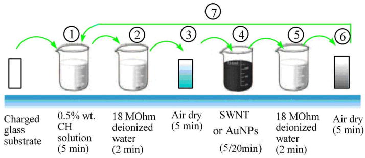
Glass slides and silicon wafers used as substrates were cleaned by immersion into “piranha” solution, 3:1 H2SO4:H2O2 (Potentially explosive when in contact with organic matter!) for one hour, followed by thorough rinsing with DI water. The deposition of (CH/SWNTs)n, where n is the number of LBL deposition cycles, was carried out by dipping the glass slides alternately into the CH solution and SWNT dispersion for five minutes using a robotic dipper Strato Sequence IV from Nanostrata Inc. Each adsorption step was separated from the next one by a two minute rinse with E-pure water. The films were blown dry with an air flow after every LBL deposition cycle, i.e. after adsorption of one CH and one SWNT layer (Figure 1). The preparation of (CH/AuNP)n films followed an identical protocol with AuNPs dispersions. The thickness the deposited composite film was characterized by Base 160 spectroscopic ellipsometer from J.A. Woollam Co, Inc.
Figure 1.
Schematics of the LBL composite synthesis from chitosan (CH) and single walled carbon nanotubes (SWNT). Assembly of gold nanoparticle (AuNP) multilayers followed the same procedure.
Patterning of (CH/SWNT)n and (CH/AuNPs)n films
LBL films on glass slides were dried at 110 °C for 10 minutes on a hot plate. Next, each slide was coated with a ~12 μm layer of AZ 9260 using a spin coater. Each slide was subjected to soft bake on a hot plate at 110 °C for three minutes. After that, the photoresist was allowed to rehydrate at room conditions for a minimum of 35 minutes. Light exposure was performed on an HTG manual aligner with an exposure time of 16 seconds. Prior to LBL sequence, an exposure series was performed on an AZ 9260 sample of the same thickness to determine optimal exposure time. After a post-exposure delay of five minutes, each sample was developed in a 1:4 AZ 400K:H2O solution for three minutes. Samples were rinsed with DI water and dried with air blow. Before etching, the film thickness was measured using a stylus profiler which was used to confirm the lithography results and to provide a baseline for tracking removal of the resist mask during etching. The films were etched with oxygen plasma in a reactive ion etcher under a chamber pressure of ~ 30 mTorr and a forward power of 100 Watts.
RESULTS AND DISCISSION
LBL assembly is one of the most effective routes for the fabrication of ultrathin nanocomposites that (a) are difficult to make by most other methods of nanocomposite synthesis; (b) suit remarkably well for the microtechnologies; and (c) can be made from a wide variety of nanoscale dispersions. Two types of nanomaterials would probably be most fundamental for electronic devices, and therefore, for patterned LBL composites: carbon nanotubes and semiconductor/metal nanoparticles (NPs). Taking, for instance carbon nanotubes,43 a wide variety of applications including high-strength structural composites,38 nanoelectronics,39 and various types of sensors40,41 are likely benefit from their outstanding electrical and mechanical properties.42 Metal and semiconductor (NPs) have attracted a great deal of attention owing to their strong dependence of optical and electronic properties on particle size.44 Gold is particularly useful in bioscience because its chemical allow for various types of custom functionalization,45 display interesting electronic effects, and have high inherent biocompatibility.46
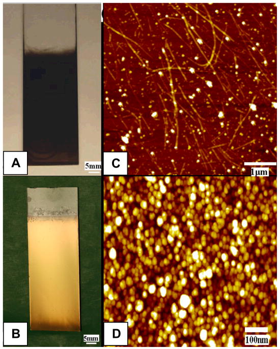
Chitosan (CH) was selected here to make nanocomposites in this work for its mechanical properties that can complement those of nanotubes and enhance those of nanoparticles. This polymer is also biocompatible, which expands the scope of potential applications even further. CH is positively charged and can be easily deposited on the negatively charged glass slides by dipping. Successive positive/negative dipping cycles alternating CH and SDS-stabilized CNTs or citrate-stabilized AuNPs yield gradually high quality LBL films following a typical linear growth model (see Supplementary information). Spectroscopic ellipsometery and scanning electron microscope (SEM) images revealed that each deposition cycle (bilayer) adds about 2 to 3 nm. The resulting film exhibits excellent homogeneity and phase integration. The representation of internal structures of LBL films can be assessed from AFM images in Figure 2 (also see Figure S2 and Figure S4 in SI). AuNPs are homogeneously distributed on the CH surface with high density. SWNT fibers display predominantly planar orientation and interconnectivity.
Figure 2.
Photographs of (A) (CH/SWNT)300 and (B) (CH/AuNP)50 composite film on a glass substrates. AFM images (C) (CH/SWNT)3 and (D) (CH/AuNP)3 deposited on silicon wafers.
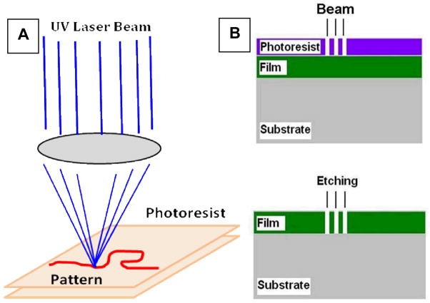
Mask-less lithography employed here utilizes tightly focused and collimated UV-laser beam to directly “write” the pattern into the photoresist. This technique is remarkable in its versatility and speed especially for the preparation of any free-hand patterns. It also has relatively high throughput and best-in-class accuracy with standard photoresists.47 It eliminates long turnaround time required for manufacturing and alignment of a mask. Additional advantage is the contact-free exposure and the possibility of a size reduction. Direct-write lithography is typically used for microoptics and microfluidics,48 and here we extend it for the preparation of composite patterns for potential utility in flexible electronics and biomedical implants. The principle difference needs to be noted between the direct patterning techniques when the materials is directly deposited/removed59 or photomodified34,58 and the methods associated with direct-write lithography. The latter term is commonly reserved for maskless methods involving photoresists and is the technique used here. Both of them have substantial advantages and (potential) areas of use. One of the most attractive points of maskless direct-write lithography is its universality which matches well with the universality of LBL assembly.
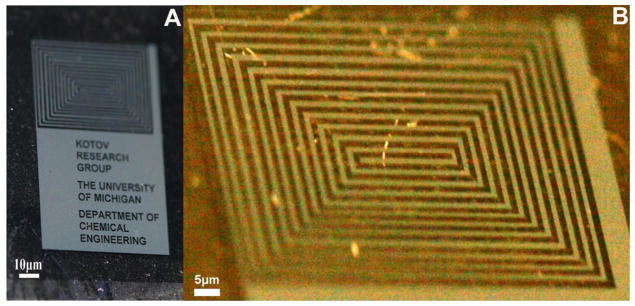
Using direct-write maskless lithography (Experimental and Supplementary Information, SI) we fabricated a prototypical concentric spiral pattern from (CH/SWNT)300 composite typically found, for instance, in RFID antennas (Figure 4A). Similar patterns could also be used in negative refractive index optics.49 The width of the line was 1 μm, while the thickness of the composite films was ca. 520 nm. Removal of the photoresists by etching does not disturb the pattern (Figure 4B). The surface of the (CH/SWNT)n film is very uniform in macroscale which is attributed to the nano- and microscopically homogeneous distribution of the SWNTs on the CH surface seen in Figure 2 and Figure S2. The resistivity of the (CH/SWNT)300 film was 6.45×10⁻⁵ Ω·m, which is approaching to the resistivity of graphite (1.3×10⁻⁵ Ω·m) indicating efficient charge transfer in the material and high interconnectivity of the nanotubes. This value of resistivity of pristine non-doped (CH/SWNT)300 films is more than two orders of magnitude lower than that of the polyaniline/SWNT composites with resistivity of 5*10−3 Ω·m50 or all-nanotube LBL thin films with a resistivity of 1*10−3 Ω·m.51 Charge transport in SWNT films can also be improved further by a variety of approaches including recently developed doping with via conjugation with π-bonds of aromatic polymers.57
Figure 4.
Photographs of prototypical spiral pattern from (CH/SWNT)300 films: (A) As-fabricated pattern before etching. (B) Pattern feature after oxygen plasma etching.
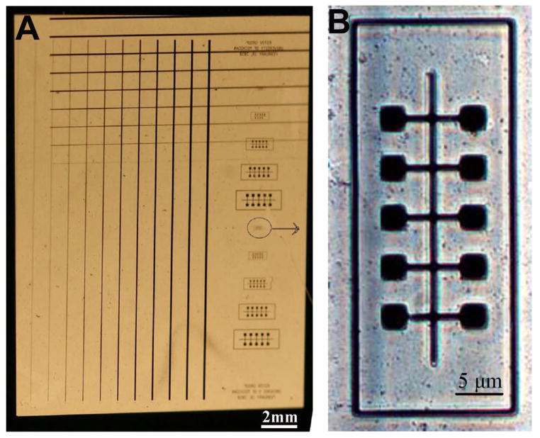
In order to accommodate the requirement of more complex devices, it is also useful to test the reasonable limits of this patterning method for nanocomposites with sequentially smaller features. (CH/SWNT)500 composite films was patterned with orthogonal arrays of lines (Figure 5A) and bus-line-and-stimulation-pads (BLASP) patterns (Figure 5B) typical for implantable neurostimulation devices.52–55 The widths of lines in the graded linear arrays were 100 μm, 90 μm, 80 μm, 70 μm, …, 10 μm, 9 μm, 8 μm, 7 μm, ···, 1 μm. In Figure 5(A), one could see the lines clearly with a width of about 6 μm. Microphotography shows that the smallest line width in the graded arrays and the smallest size of squares in the BLASP patterns were obtained to be 1 μm and 2.5 μm, respectively (Figure 5A, B). This is probably not yet the absolute limit of resolution for the material. There are no “meniscus corners” in the crossing parts; this fact indicates that the (CH/SWNT)n films exhibit excellent mechanical adhesion to the substrate. On the other hand, the round corners of the square contact pads in BLASP patterns indicate that we are approaching the limit the for direct-write patterning method. Although the BLASP pattern in Figure 5B appears to be clearly defined we need to point out the remnants of the SWNT composite in the etched areas. This observation indicates the need to further optimize the etching step for (CH/SWNT)500 films. Its strong adhesion to the substrate necessitates probably more energetic and/or longer treatment with oxygen plasma, which can certainly be accomplished.
Figure 5.
(A) Photograph of (CH/SWNT)500 films on a glass substrate patterned with orthogonal linear array. (B) Microscale photography image of the encircled part (A) with bus-line-and-stimulation-pads (BLASP) pattern.
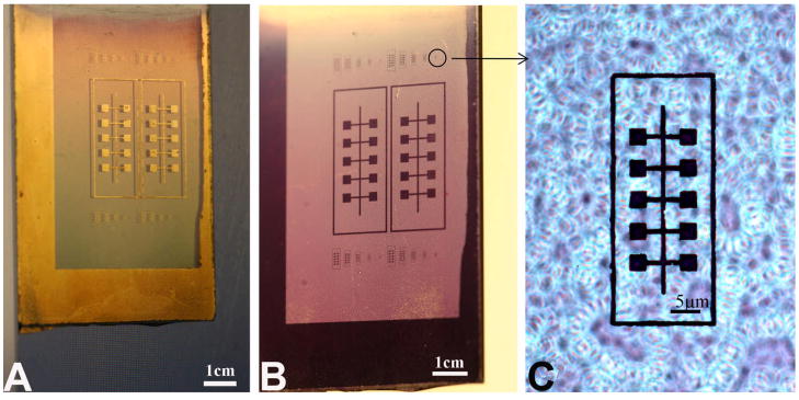
Let us look now at the patterns made for (CH/AuNP)n composite films. They also revealed equally high or even better quality patterns (Figure 6) as those made by direct-write lithography from (CH/SWNT)n composites. The surface of the (CH/AuNP)n film is highly reflective which was attributed to the homogeneously distributed Au NPs (Figures 2, S4, S5) and high mobility of electrons. Indeed, the resistivity of the (CH/AuNP)50 film was 3.80×10⁻⁶ Ω·m at 20 °C. This is more than one order of magnitude lower than resistivity obtained for SWNT films and two orders of magnitude higher than the resistivity of bulk gold, i.e. 2.05×10⁻⁸ Ω·m. Resistivity of (CH/AuNP)50 film composite is comparable to that of resistive alloys, such as nichrome, 1.10×10⁻⁶ Ω·m. In respect to potential applications such electrical properties combined with mechanical properties of composites and low temperature processing compatible with many plastics could be exceptionally promising for flexible MEMS and actuators.
Figure 6.
(A, B) Photographs of BLASP patterns with sequentially smaller features made on (CH/AuNP)50 films at different illumination angles. (C) Microscale photography images of the circled part in (B)
The smallest width of interconnecting lines for patterns on (CH/AuNP)n composites was again 1 μm and was limited only by the resolution of the direct-write patterning instrument (see Experimental). Also note that the smallest 2.5 μm squares in the BLASP pattern have nearly ideal shape without any noticeable rounding or “meniscus corners”. High-magnification optical micrographs do not show any remnants of the composite film on the glass substrate (Figure 6C) and therefore, indicative efficient and accurate etching process.
CONCLUSIONS and PERSPECTIVES
(CH/SWNT)n and (CH/AuNP)n were successfully patterned using direct-write lithography. This approach based on the LBL films is applicable to a wide range of functional materials and their contents in polymer matrix. The integrated nanocomposite+lithography technology may provide multifunctional molecular assemblies of tailored architectures and material properties for various devices for which the combination of mechanical and electrical properties is of particular importance. The universality of the method allowing one to “construct” a material and the pattern according to the specifications is of importance. The next steps of the research in this fundamental direction should be integration the following: (a) demonstration of integrated micromanufactured devices using described composites utilizing their electrical properties; (b) preparation of the bridge and other basic structures typical for MEMS devices; (c) realization of multipass lithography and incorporation of multiple composite materials into a microscale architecture; and (d) utilization of electrically-driven optical effects in visible (nanoparticles) or infra-red (nanowires and nanotubes) associated with adsorption, emission, reflection, or scattering of nanocomposites or their (sub)micron scale elements. In respect to practical side of nanocomposite+lithography technology, biomedical application and, in particularly, implantable devices, requiring both tissue compliance and electrical functionalities present strong motivation for their further development. Neuroprosthetic devices18 need innovations in respect to materials and manufacturing techniques in (sub)micron scale particularly badly. The direct-write capabilities of the described lithography and its versatility are likely to be particularly advantageous for personalization of such devices. Applications in sensing will face strong competition with already developed micro- and nanoscale technologies involving nanomaterials. Nanocomposite microscale circuits will have to demonstrate unusual advantages potentially in the realm of flexible circuits. We also see large potential for the discovery of novel optical phenomena taking advantage of the electrically responsive energy states of nanoparticles, nanotube, etc. Variable scattering properties and mechanics of microscale structures can offer a new toolbox for thin optical devices.
Supplementary Material
Figure 3.
Schematics of direct write (maskless) lithography and patterning scheme used in this study.
Acknowledgments
The authors are indebted to Dr. Brian N. Johnson and Prof. Mark A. Burns for the helping with direct-write patterning instruments. We greatly acknowledge financial assistance by China Scholarship Council and the Fundamental Research Funds for the Central Universities (LZUjbky-2010-78) for this work. The work was also supported by AFOSR grants FA9550-08-1-0382, GRT00008581/RF60012388, MURI 444286-P061716. We also acknowledge the support from NSF under grant ECS-0601345; EFRI-BSBA 0938019; CBET 0933384; and CBET 0932823 and from National Institutes of Health under NIH 1R21CA121841-01A2. Any opinions, findings, and conclusions or recommendations expressed in this material are those of the authors and do not necessarily reflect the views of the National Science Foundation or National Institutes of Health. This material is based upon work partially supported by the Center for Solar and Thermal Energy Conversion, an Energy Frontier Research Center funded by the U.S. Department of Energy, Office of Science, Office of Basic Energy Sciences under Award Number #DE-SC0000957. The authors thank the University of Michigan’s EMAL for its assistance with electron microscopy, and for the NSF grant #DMR-9871177 for funding for the JEOL 2010F analytical electron microscope used in this work.
References
- 1.Huo FW, Zheng ZJ, Zheng GF, Giam LR, Zhang H, Mirkin CA. Science. 2008;321:1658. doi: 10.1126/science.1162193. [DOI] [PMC free article] [PubMed] [Google Scholar]
- 2.Ginger DS, Zhang H, Mirkin CA. Angew Chem Int Ed. 2004;43:30. doi: 10.1002/anie.200300608. [DOI] [PubMed] [Google Scholar]
- 3.Li Y, Wu Y, Ong BS. J Am Chem Soc. 2005;127:3266. doi: 10.1021/ja043425k. [DOI] [PubMed] [Google Scholar]
- 4.Li Y, Wu Y, Ong BS. J Am Chem Soc. 2007;129:1862. doi: 10.1021/ja067596w. [DOI] [PubMed] [Google Scholar]
- 5.Mirkin CA. ACS Nano. 2007;79:1. doi: 10.1021/nn700228m. [DOI] [PubMed] [Google Scholar]
- 6.Salaita K, Wang YH, Mirkin CA. Nat Nanotechnol. 2007;145:2. doi: 10.1038/nnano.2007.39. [DOI] [PubMed] [Google Scholar]
- 7.Tranquada JM, Woo H, Perring TG, Goka H, Gu GD, Xu G, Fujita M, Yamada K. Nature. 2004;429:538. doi: 10.1038/nature02574. [DOI] [PubMed] [Google Scholar]
- 8.Xia Y, Whitesides GM. Annu Rev Mater Science. 1998;153:28. [Google Scholar]
- 9.Martinez ED, Bellino MG, Soler-Illia GJAA. ACS Appl Mater Inter. 2009;1:746. doi: 10.1021/am900018j. [DOI] [PubMed] [Google Scholar]
- 10.Chang TL, Cheng KY, Chou TH, Su CC, Yang HP, Luo SW. Microelectronic Eng. 2009;86:874. [Google Scholar]
- 11.Wu P, Du N, Zhang H, Jin L, Yang D. Mater Chem Phys. 2010;124:908. [Google Scholar]
- 12.Wang PT, Guo JB, Wang HH, Zhang Y, Wei J. J Phys Chem C. 2009;113:8118. [Google Scholar]
- 13.Meyer JC, Girit CO, Crommie MF, Zettl A. Appl Phys Lett. 2008;92:123110. [Google Scholar]
- 14.Lin KL, Jain K. Ieee Electr Device L. 2009;30:14. [Google Scholar]
- 15.Cao Q, Kim H, Pimparkar N, Kulkarni JP, Wang CJ, Shim M, Roy K, Alam MA, Rogers JA. Nature. 2008;454:495. doi: 10.1038/nature07110. [DOI] [PubMed] [Google Scholar]
- 16.Jonnalagadda K, Cho SW, Chasiotis I, Friedmann T, Sullivan J. J Mech Phys Solids. 2008;2:388. [Google Scholar]
- 17.Bush B, Xu GH, Carraro C, Maboudian R. Sensor Actuata A-Phys. 2006;126:194. [Google Scholar]
- 18.Kotov NA, Winter JO, Clements IP, Jan E, Timko BP, Campidelli S, Pathak S, Mazzatenta A, Lieber CM, Prato M, Bellamkonda RV, Silva GA, Kam NWS, Patolsky F, Ballerini L. Adv Mater. 2009;21:3970. [Google Scholar]
- 19.Srivastava S, Kotov NA. Acc Chem Res. 2008;41:1831. doi: 10.1021/ar8001377. [DOI] [PubMed] [Google Scholar]
- 20.Kozlovskaya V, Kharlampieva E, Jones K, Lin ZQ, Tsukruk VV. Langmuir. 2010;26:7138. doi: 10.1021/la9042099. [DOI] [PubMed] [Google Scholar]
- 21.Aldea G, Gutierrez H, Nunzi JM, Chitanu GC, Sylla M, Simionescu BC. Opt Mater. 2009;29:1640. [Google Scholar]
- 22.Shim JS, Yun YH, Cho W, Shanov V, Schulz MJ, Ahn CH. Langmuir. 2010;26:11642. doi: 10.1021/la101079b. [DOI] [PubMed] [Google Scholar]
- 23.Seo J, Schattling P, Lang T, Jochum F, Nilles K, Theato P, Char K. Langmuir. 2010;26:1830. doi: 10.1021/la902574z. [DOI] [PubMed] [Google Scholar]
- 24.Shim BS, Zhu J, Jan E, Critchley K, Ho S, Podsiadlo P, Sun K, Kotov NA. ACS Nano. 2009;3:1711. doi: 10.1021/nn9002743. [DOI] [PubMed] [Google Scholar]
- 25.Shim BS, Kotov NA. Langmuir. 2005;21:9381. doi: 10.1021/la050992s. [DOI] [PubMed] [Google Scholar]
- 26.Shim BS, Podsiadlo P, Lilly DG, Agarwal A, Lee J, Tang Z, Ho S, Ingle P, Paterson D, Lu W, Kotov NA. Nano Lett. 2007;7:3266. doi: 10.1021/nl071245d. [DOI] [PubMed] [Google Scholar]
- 27.Park J, Hammond PT. Adv Mater. 2006;16:520. [Google Scholar]
- 28.Harris JJ, DeRose PM, Bruening ML. J Am Chem Soc. 1999;121:1978. [Google Scholar]
- 29.Yang SY, Rubner MF. J Am Chem Soc. 2002;124:2100. doi: 10.1021/ja017681y. [DOI] [PubMed] [Google Scholar]
- 30.Im S, Kim BS, Lee LH, Tenhaeff WE, Hammond PT, Gleason KK. Macromol Rapid Commun. 2008;29:1648. [Google Scholar]
- 31.Im SG, Bong KW, Kim BS, Baxamusa SH, Hammond PT, Doyle PS, Gleason KK. J Am Chem Soc. 2008;130:14424. doi: 10.1021/ja806030z. [DOI] [PubMed] [Google Scholar]
- 32.Cui TH, Hua F, Lvov Y. Sensor Actuat A-phys. 2004;114:501. [Google Scholar]
- 33.Hua F, Shi J, Lvov Y, Cui T. Nano Lett. 2002;2:1219. [Google Scholar]
- 34.Wang Y, Tang ZY, Correa-Duarte MA, Liz-Marzán LM, Kotov NA. J Am Chem Soc. 2003;125:2830. doi: 10.1021/ja029231r. [DOI] [PubMed] [Google Scholar]
- 35.Yoo PJ, Nam KT, Belcher AM, Hammond PT. Nano Lett. 2008;8:1081. doi: 10.1021/nl073079f. [DOI] [PubMed] [Google Scholar]
- 36.Andres CM, Kotov NA. J Am Chem Soc. 2010;132:14496. doi: 10.1021/ja104735a. [DOI] [PMC free article] [PubMed] [Google Scholar]
- 37.Granick S, Sukhishvili SA. J Am Chem Soc. 2000;122:9550. [Google Scholar]
- 38.Andrews R, Jacques D, Rao AM, Rantell T, Derbyshire F, Chen Y, Chen J, Haddon RC. Appl Phys Lett. 1999;75:1329. [Google Scholar]
- 39.Tsukagoshi K, Yoneya N, Uryu S, Aoyagi Y, Kanda A, Ootuka Y, Alphenaar BW. Physica B. 2002;323:107. [Google Scholar]
- 40.Wood JR, Zhao Q, Frogley MD, Meurs ER, Prins AD, Peijs T, Dunstan DJ, Wagner HD. Phys Rev B. 2001;62:7571. [Google Scholar]
- 41.Kong J, Franklin NR, Zhou C, Chapline MG, Peng S, Cho K, Dai H. Science. 2000;287:622. doi: 10.1126/science.287.5453.622. [DOI] [PubMed] [Google Scholar]
- 42.Baughman RH, Zakhidov AA, De Heer WA. Science. 2002;297:787. doi: 10.1126/science.1060928. [DOI] [PubMed] [Google Scholar]
- 43.Iijima S. Nature. 1991;354:56. [Google Scholar]
- 44.Eustis S, El-Sayed M. Chem Soc Rev. 2006;35:209. doi: 10.1039/b514191e. [DOI] [PubMed] [Google Scholar]
- 45.Wang K, Schonbrun E, Crozier KB. Nano Lett. 2009;9:2623. doi: 10.1021/nl900944y. [DOI] [PubMed] [Google Scholar]
- 46.Ofir Y, Samanta B, Rotello VM. Chem Soc Rev. 2008;37:1814. doi: 10.1039/b712689c. [DOI] [PubMed] [Google Scholar]
- 47.Pieter K. 6919952 United States Patent.
- 48.Piqué A, Chrisey DB. Direct-write technologies for rapid prototyping applications: sensors, electronics, and integrated power sources. Academic Press; 2002. [Google Scholar]
- 49.Smith D, Pendry JB, Wiltshire MCK. Science. 2004;305(5685):788–792. doi: 10.1126/science.1096796. [DOI] [PubMed] [Google Scholar]
- 50.Blanchet GB, Fincher CR, Gao F. Appl Phys Lett. 2003;82:1290. [Google Scholar]
- 51.Lee SW, Kim BS, Chen S, Shao-Horn Y, Hammond PT. J Am Chem Soc. 2009;131:671. doi: 10.1021/ja807059k. [DOI] [PubMed] [Google Scholar]
- 52.Coffey RJ. Artificial Organs. 2009;33:208. doi: 10.1111/j.1525-1594.2008.00620.x. [DOI] [PubMed] [Google Scholar]
- 53.Shellock FG. J Magn Reson Imaging. 2002;16:465. doi: 10.1002/jmri.10207. [DOI] [PubMed] [Google Scholar]
- 54.Mazzatenta A, Giugliano M, Campidelli S, Gambazzi L, Businaro L, Markram H, Prato M, Ballerini L. J Neurosci. 2007;27:6931. doi: 10.1523/JNEUROSCI.1051-07.2007. [DOI] [PMC free article] [PubMed] [Google Scholar]
- 55.Malarkey EB, Reyes RC, Zhao B, Haddon RC, Parpura V. Nano Lett. 2008;8:3538. doi: 10.1021/nl8017912. [DOI] [PMC free article] [PubMed] [Google Scholar]
- 56.Storhoff JJ, Elghanian R, Mucic CA, Letsinger RL. J Am Chem Soc. 1998;120:1959. [Google Scholar]
- 57.Zhu J, Shim BS, Prima MD, Kotov NA. J Am Chem Soc. 2011;133(19):7450–7460. doi: 10.1021/ja111687t. [DOI] [PMC free article] [PubMed] [Google Scholar]
- 58.Radha B, Kiruthika S, Kulkarni GU. J Am Chem Soc. 2011;133:12706. doi: 10.1021/ja2039612. [DOI] [PubMed] [Google Scholar]
- 59.Ki-Bum Lee K-B, Lim J-H, Chad A, Mirkin CA. J Am Chem Soc. 2003;125:5588–5589. doi: 10.1021/ja034236p. [DOI] [PubMed] [Google Scholar]
Associated Data
This section collects any data citations, data availability statements, or supplementary materials included in this article.


