Abstract
An in situ platform for characterizing plasma-materials interactions at the nanoscale in the transmission electron microscope (TEM) has been demonstrated. Integrating a DC microplasma device, having plane-parallel electrodes with a 25 nm thick Au film on both the cathode and anode and operating in 760 Torr of Ar, within a TEM provides real-time observation of Au sputtering and island formation with a spatial resolution of < 100 nm. Analyses of TEM and atomic force microscopy images show the growth of Au islands to proceed by a Stranski-Krastanov process at a rate that varies linearly with the discharge power and is approximately a factor of 3 larger than the predictions of a DC plasma sputtering model. The experiments reported here extend in situ TEM diagnostics to plasma-solid and plasma-liquid interactions.
Plasma-materials interactions are fundamental to the synthesis and performance of numerous materials and fabrication processes, respectively. Realizing nanoscale versions of tubes, wires, cones and belts, for example, often relies on plasma processing1,2,3,4, and the contributions of nonequilibrium plasmas to lighting5, semiconductor device fabrication6, and the disinfection of biological tissue7 are difficult to overstate. Owing to the localized and nonlinear nature of plasma-materials interactions, however, the current understanding of the associated physical mechanisms is limited. Compounding the problem is the availability of few tools capable of directly observing such processes, particularly when probing the growth of nanomaterials of increasing technological interest. Consequently, gaining a deeper understanding of plasma-materials interactions at the nanoscale requires new approaches to surface characterization at the relevant spatial scale and in the presence of a challenging environment.
This Communication describes the implementation of an in situ platform for probing plasma-materials interactions with sub-100 nm spatial resolution by integrating a microplasma device8 with a transmission electron microscope (TEM). Argon plasma, generated between two Au films separated by 75 μm, in an enclosed environmental cell provides a versatile tool with which the sputtering and deposition of metal (for example) can be observed in real-time with unprecedented resolution. Data presented here demonstrate that the rate for Au deposition on the microplasma device anode varies linearly with the power deposited into the plasma and the experimental measurements correlate well with a theoretical model for sputtering in a DC plasma. In situ TEM was first demonstrated in 1942 (Ref. 9) but, in recent years, several environmental cell TEM techniques have been developed for examining fundamental physical and chemical processes in the gas and liquid phases10,11,12. The sputtering/deposition microcell adopted here extends in situ TEM techniques to the investigation of plasma-solid and plasma-liquid interactions by incorporating Au-coated windows having an overall thickness of ~300 nm and separated by 75 μm. Such a cell allows for direct observations of both metal sputtering and deposition in the prototypical Ar-Au system to be made in situ to the microscope and in real time.
Results
Dynamics of gold film sputtering and island formation
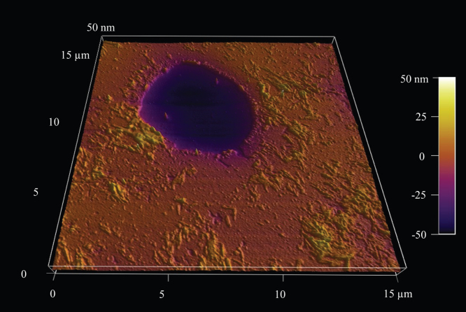
Sputtering of a gold film by Ar ions arriving at the cathode surface is evident in the timelapse (the in-situ TEM video of the plasma-sputtering of a gold cathode film is shown in S1), bright field images of Fig. 1 (and S2). Results are presented as false-color maps acquired at t = 0 (panel (a)) as well as 13 min, 26 min, and 42 min after the initiation of processing. In recording these data, the voltage imposed across the two electrodes of Fig. 6 was fixed at 400 VDC. It should be noted that the dark circles are contaminant particles having diameters ≤150 nm. From the normalized image pixel profile of Fig. 1 and the sample thickness, the sputtering rate for the Au film is calculated to be 1.2 × 10⁻² nm–s−1 when the power deposited in the plasma is ~28 mW. It is clear from Fig. 1 that strong preferential etching of the Au film is observed in the immediate vicinity of the contaminant particles. This conclusion is borne out specifically by panel (b) of Fig. 1 in which the onset of etching is visible around each of the larger particles, which presumably are dielectric. Charging of such nanoparticles by the plasma alters dramatically the local electric field strength which is responsible for inducing localized gas and solid phase reactions. Once initiated at the particles, etching quickly emanates outward (indicated by the white arrows) and eventually envelops much of the exposed surface of the cathode. The data of Fig. 1 provide a vivid example of the benefits of in situ TEM for visualizing and analyzing local processes at the <200 nm scale. Ex situ AFM scans of the Au film surface at the cathode are consistent with the TEM images of Fig. 1. As shown by the AFM topographic map of Fig. 2, the surface is rough and depressions that often penetrate the entire film are observed.
Figure 1. Time-lapse, false-color TEM images of the sputtering of a gold cathode film.
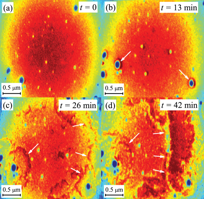
Results are given for t = 0 (panel (a)), 13 min, 26 min, and 42 min following the onset of processing. Note that the dark circles are contaminant particles having diameters ≤150 nm, and the white arrows indicate regions of preferential etching.
Figure 6. Diagram in cross-section of the in situ plasma microcell.
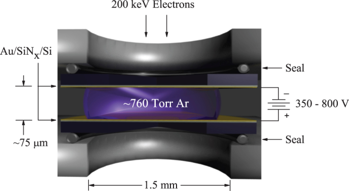
Si-supported SiNx membranes, coated on their interior faces with 25–50 nm of Au, serve both as TEM windows and electrodes. These windows/electrodes are separated by 75 μm and the region between them contains ~760 Torr of Ar.
Figure 2. False color topographic map, recorded by ex situ AFM, of a 15 × 15 μm2 sputtered region at the cathode.
False-color TEM images, similar to those of Fig. 1 but captured for a region of the SiNx anode surface that was partially masked by two adjacent polystyrene spheres, are shown in Fig. 3 (S3, S4 and S5). Presented as snapshots representative of the deposition process, the four images of Fig. 3 were recorded at t = 0 (initiation of the plasma), 5 s, 38 s, and 2.5 min. For these experiments, the discharge voltage and power delivered to the plasma (700 VDC and ~80 mW, respectively) were maintained at levels higher than those of Fig. 1 for the purpose of accelerating the growth process. Gold deposits initially in the uncoated (masked) circular regions of the anode as broad, thin films situated primarily near the center. This initial growth phase is attributable primarily to neutral Au atoms liberated by Ar+ bombardment of the cathode. Within seconds of the start of the deposition process, signs of island formation are observed. De-wetting of the broad thin films and the appearance of small islands (sub-20 nm) as early as t = 5 s is presumably the result of Au surface diffusion driven by interfacial energy considerations. Such kinetics closely resemble the Stranski-Krastanov growth mode in which the growth process is characterized by a transition from layer deposition to adatom clusters and islands when the layer thickness reaches a critical value. In the present experiments, formation of the critical precursor film is, indeed, observed immediately after ignition of the microplasma, and the island growth mode follows shortly thereafter.
Figure 3. False-color TEM images similar to those of Fig. 1 but recorded for a region of the anode surface (shown in red) that had been partially masked by polystyrene spheres.
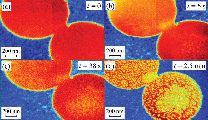
Data are presented for: (a) t = 0; (b) t = 5 s; (c) t = 38 s, and (d) t = 2.5 minutes following the start of the growth process. Island formation is evident at the later stages of the growth process.
Ex situ AFM scans of uncoated regions of the anode surface, similar to that of Fig. 2 for the cathode, corroborate the phenomena described above. Fig. 4 is a tomographic map, displayed in false color, of the morphology of a film deposited onto another circular, initially-uncoated region produced on the anode surface by a polystyrene sphere. Preferential nucleation of Au at the periphery of the 1 μm diameter circle is evident but film growth is also occurring at the center of the uncoated substrate region, as documented previously in Fig. 3. Based on feature height measurements from the AFM data, the Au island morphology appears to be that of truncated spheres. For the experimental conditions of Fig. 3 (700 VDC discharge bias, ~80 mW deposited power), an area-normalized growth rate of 3 × 10⁻² nm-s−1 was extracted from both the TEM and AFM images. When the discharge voltage and power are increased to 800 VDC and ~100 mW, respectively, the normalized growth rate rises to ~3.7 × 10⁻² nm-s−1.
Figure 4. AFM tomographic map, shown in false color and analogous to that of Fig. 2 except that the data were obtained in the vicinity of a circular, uncoated region on the anode.
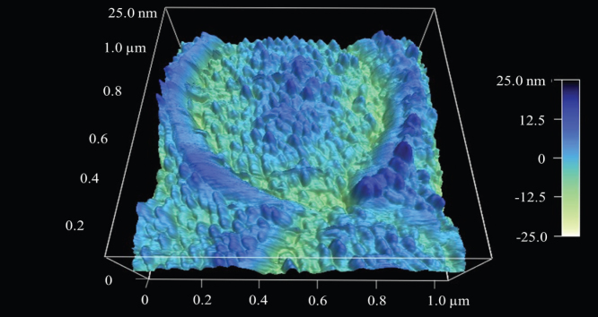
The calibration scale at right spans a range of 50 nm.
Discussion
To interpret the measured island growth rates, we adopt the expression proposed by Stutzin et al.13 for the rate of film growth due to sputtering in a parallel plate, DC discharge:
where Pd is the discharge power density, <xth> is the mean thermalization distance for an atom, G is the anode-cathode gap between the two parallel electrodes of Fig. 6, ρ is the atomic number density for the deposited film, γ is the secondary electron emission coefficient, Es is the average sputtering energy for the material under study, and q is the magnitude of the charge on an electron. This expression, based upon a diode model, predicts the primary experimental trends observed in these and other experiments-namely, the linear variation of the film deposition rate with power deposited into the plasma, and the inverse dependence of R on the anode gap G. Although explicit measurements of several of the variables in equation (1) are not available in the literature, all are readily estimated and, in accord with Ref. 13, we take γ, Es, and <xth> to be 0.2, ~1 keV, and 60 mTorr-cm/P (for Ar, where P is the gas pressure expressed in Torr), respectively.
Fig. 5 summarizes both theory and experimental measurements of the dependence of the Au island growth rate on the power dissipated by the microplasma. The solid line represents the prediction of equation (1) [Ref. 13], assuming the values for γ, Es, and <xth> to be those presented earlier. Experimental data are indicated by the open circles ( ) and the error bars associated with each point reflect the estimated uncertainty for that measurement. The broken line is included in Fig. 5 to indicate that theory and experiment differ by a factor of ~3. However, considering: 1) the cumulative uncertainty introduced by several parameters in equation (1), and 2) the value for <xth> cited in Ref. 13 has been measured at Ar pressures considerably lower than those of interest here, one concludes that the factor of 3 discrepancy between theory and experiment in Fig. 5 can be viewed as reasonable agreement.
Figure 5. Dependence of Au island growth rate on the power delivered to the microdischarge.
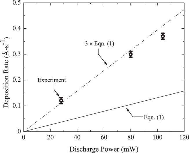
The solid line represents the predictions of equation (1), assuming the values for several parameters to be those cited in the text. Experimental results are indicated by open circles and error bars reflect the estimated uncertainty in each measurement. The broken line demonstrates that theory and experiment differ by a factor of ~3.
In summary, experiments have been described in which a microplasma has been generated in situ with to a TEM. The growth rate for Au islands was measured and found to correlate well with a diode model for DC sputtering and deposition in parallel plate geometry. Integration of a low temperature plasma with a TEM presents new opportunities in the science of plasma-materials interactions. Extending the present experiments to RF excitation of the plasma, and alternative window materials, will permit oxidizing environments to be investigated and, specifically, offers the ability to explore reaction pathways in specific materials systems. Furthermore, lattice images have already been obtained in the absence of the electric field imposed on the microplasma device. Continued effort to screen the microscope from spurious field effects will undoubtedly yield high-resolution lattice images in real-time and provide a window onto the reaction kinetics.
Methods
Design of plasma cell
A cross-sectional diagram of the design for the plasma microcell developed for the present experiments is illustrated in Fig. 6. Commercially-available, Si-supported SiNx membranes having Si grid and SiNx thicknesses of 200 nm and 50 nm, respectively, served as the windows for the cell. Gold films, 25–50 nm in thickness, were deposited onto the interior faces of both windows by electron beam evaporation. Prior to the Au film growth process, ~1 μm diameter polystyrene spheres were placed onto several of the windows to act as deposition masks. After the Au films were deposited, the spheres were removed with acetone and a deionized water rinse, thereby exposing regions in which the window was uncoated. These circular openings in the gold film proved to be ideal for observing the temporal history of the plasma-induced deposition process. Gold contact pads were patterned onto the outside (rear) face of both windows and Au wires were subsequently bonded onto the pads. The Au-coated Si/SiNx windows were separated by 75 μm with spacers and the planar region between the windows was filled with 1 atm (~760 Torr) of Ar in a glovebox prior to sealing the structure. Before finalizing the assembly, the windows were placed in the Ar-filled glovebox for 24 hours. Tests showed that this procedure yields microcells containing either a gas or a liquid that are stable in the vacuum environment of the TEM. For all of the experiments described here, the windows/electrodes were driven by a power supply delivering 350–800 VDC through a 1 MΩ resistor in series with the anode. Current supplied to the plasma was determined from the voltage developed across a 1 kΩ resistor. When the microcell was powered, the violet glow characteristic of Ar was readily visible through the 1.5 mm apertures at the top and bottom of the cell structure (S6).
Completed microcell assemblies were installed in a JEOL-2010 LaB6 microscope having a video capture system. Morphology of the anode and cathode gold films was examined at several stages of the sputtering and deposition process by ex situ atomic force microscopy (AFM).
Monte Carlo simulations (Electron Flight Simulator) predict that ~3% of the 200 keV electrons incident on the microcell scatter inelastically. Based upon the electron fluxes utilized in these experiments (beam current density of ~1.5 mA-cm−2), the fraction of the gas atoms in the cell ionized by the particle beam is ~10−8 which is negligible compared to that generated by the plasma itself (~10−6 for an estimated electron density of ~1013 cm−3).
Author Contributions
K.T. and S.J.D. conceptualized, planned, and coordinated the study. K.T. and T.J.H. designed the cell and analyzed the data. K.T. conducted the experiments. J.G.E. analyzed the TEM images and wrote the manuscript.
Supplementary Material
Supporting materials_Figures
Supporting materials_Video_1
Supporting materials_Video_2
Acknowledgments
K.T. and S.J.D. gratefully acknowledge funding provided by the U.S. Department of Energy, Basic Energy Sciences (Contract No. DE-SC0006509). T.J.H. and J.G.E. gratefully acknowledge the support of the U.S. Air Force Office of Scientific Research and the National Science Foundation under grant nos. FA9550-10-1-0048 and CBET 08-53739, respectively.
References
- Sunkara M. K., Sharma S., Miranda R., Lian G. & Dickey E. C. Bulk synthesis of silicon nanowires using a low-temperature vapor-liquid-solid method. Appl. Phys. Lett. 79, 1546 (2001). [Google Scholar]
- Hofmann S., Ducati C., Robertson J. & Kleinsorge B. Low-temperature growth of carbon nanotubes by plasma-enhanced chemical vapor deposition. Appl. Phys. Lett. 83, 135 (2003). [Google Scholar]
- Ostrikov K. Colloquium: reactive plasmas as a versatile nanofabrication tool. Rev. Mod. Phys. 77, 489 (2005). [Google Scholar]
- Chiang W.-H. & Sankaran R. M. Linking catalyst composition to chirality distributions of as-grown single-walled carbon nanotubes by tuning NixFe1−x nanoparticles. Nature Mat. 8, 882 (2009). [DOI] [PubMed] [Google Scholar]
- Eden J. G., Park S.-J., Herring C. M. & Bulson J. M. Microplasma light tiles: thin sheet lamps for general illumination. J. Phys. D 44, 224011 (2011). [Google Scholar]
- Lieberman M. A. & Lichtenberg A. J. Principles of Plasma Discharges and Materials Processing, 2nd ed. (Wiley – Interscience, 2005). [Google Scholar]
- Yu H., Perni S., Shi J. J.,Wang D. Z., Kong M. G. & Shama G. Effects of cell surface loading and phase of growth in cold atmospheric gas plasma inactivation of Escherichia coli K12. J. Appl. Microbiol. 101, 1323 (2006). [DOI] [PubMed] [Google Scholar]
- Becker K. H., Schoenbach K. H. & Eden J. G. Microplasmas and applications. J.Phys. D 39, R55–R70 (2006). [Google Scholar]
- Ruska E. Beitrag zur übermikroskopischen Abbildung bei höheren Drucken. Kolloid Z. 100, 212 (1942). [Google Scholar]
- Sun L., Noh K. W., Wen J.-G. & Dillon S. J. In-situ transmission electron microscopy observation of silver oxidation in ionized/atomic gas. Langmuir 27, 14201 (2011). [DOI] [PubMed] [Google Scholar]
- Noh K. W., Liu Y., Sun L. & Dillon S. J. Challenges associated with in-situ TEM in environmental systems: the case of silver in aqueous solutions. Ultramicroscopy 116, 34 (2012). [Google Scholar]
- deJonge N. & Ross F. M. Electron microscopy of specimens in liquid. Nature Nanotech. 6, 695 (2011). [DOI] [PubMed] [Google Scholar]
- Stutzin G. C., Rózsa K. & Gallagher A. Deposition rates in direct current diode sputtering. J. Vac. Sci. Technol. A 11, 647 (1993). [Google Scholar]
Associated Data
This section collects any data citations, data availability statements, or supplementary materials included in this article.
Supplementary Materials
Supporting materials_Figures
Supporting materials_Video_1
Supporting materials_Video_2


