Abstract
This work describes a simple, versatile, and inexpensive procedure to prepare optically transparent carbon electrodes, using proteins as precursors. Upon adsorption, the protein-coated substrates were pyrolyzed under reductive conditions (5% H2) to form ultra-thin, conductive electrodes. Because proteins spontaneously adsorb to interfaces forming uniform layers, the proposed method does not require a precise control of the preparation conditions, specialized instrumentation, or expensive precursors. The resulting electrodes were characterized by a combination of electrochemical, optical, and spectroscopic means. As a proof-of-concept, the optically-transparent electrodes were also used as substrate for the development of an electrochemical glucose biosensor. The proposed films represent a convenient alternative to more sophisticated, and less available, carbon-based nanomaterials. Furthermore, these films could be formed on a variety of substrates, without classical limitations of size or shape.
1. Introduction
Carbon-based nanomaterials have proven essential to the development of a wide range of technological applications in physics, chemistry, biology, and engineering.1 Besides their high mechanical strength, low weight, exposed area, roughness, and electron distribution,2 their ability to promote interactions with biological entities3-5 have allowed the application of carbon-based nanomaterials into a variety of analytical processes.6 Although many carbon allotropes have been used, carbon nanotubes (CNT) are amongst the most widely reported.7 Due to their wide potential window, low background current, and relatively low cost, CNT have been of particular interest to the development of electrochemical biosensors.8-9 In most cases, the basic structure resembles that of graphite and is composed of layers of sp2-bonded carbon atoms yielding to the formation of a weakly delocalized π-electron cloud. This configuration is responsible for the good electrical conductivity, the capacity to form charge-transfer complexes when in contact with electron donor groups,7 and the plasmon resonance observed in some of these structures.10 A variety of processes including vacuum filtration, spin coating, dip coating, Langmuir–Blodgett deposition, spray-coating, and press-transfer have been used to fabricate transparent films of CNT.11-15 Although great progress has been recently made in the fabrication of CNT,16 one common limitation for their use is the difficulty to obtain multiple batches with uniform chemical and physical properties. This problem has been pointed as one of the major challenges limiting commercialization of CNT-based devices17 and, not surprisingly, also affects other popular forms of carbon-based nanomaterials such as graphene.18 To overcome such deficiencies, alternative materials should be developed. Among them, optically transparent carbon electrodes (OTCE) are particularly attractive because they offer properties that are similar to those of carbon nanotubes including good electrical conductivity, high stability in acidic and basic solutions, wide potential window, and adequate robustness.19-22 Although OTCE can be systematically fabricated by reduction at high temperature of photoresists;20, 23-24 a precise control of the preparation conditions, specialized instrumentation, or expensive precursors25-26 are typically required to strike an adequate balance between optical transparency and electrical resistivity of the films.27-29
In addition, these films must often be deposited on conductive (or semiconductive) substrates such as gold, platinum, or indium-tin oxide19 further complicating its analysis by spectroscopic means. The immediate consequence of these drawbacks is the reduced availability and limited applicability of OTCE. In order to bolster the development of new applications, alternative methods for the fabrication of ultra-thin OTCE are currently required. Such methods should be versatile, reliable, and amenable to standard laboratory set-ups. Considering such critical need, this manuscript describes the fabrication of nanostructured, uniform, transparent, and conductive OTCE obtained by pyrolysis of biological precursors. These precursors (e.g. proteins) were selected based on their characteristics (elemental composition, size, solubility, and cost) and deposited on solid substrates by simple adsorption from an aqueous solution. The resulting electrodes were characterized in terms of topographical, optical, and electrochemical properties and used for the development of an electrochemical biosensor for glucose.
2. Experimental Section
Reagents and Solutions
All chemicals were analytical reagent grade and used as received. All aqueous solutions were prepared using 18 MΩ·cm water (NANOpure Diamond, Barnstead; Dubuque, IA). Hydrogen peroxide, sodium hydroxide, and α-D-glucose were purchased from Fisher Scientific (Fair Lawn, NJ). K3Fe(CN)6 and Ru(NH3)6Cl3 were purchased from Sigma-Aldrich (Saint Louis, MO). Bovine serum albumin (BSA, 66.5 KDa, Fraction V) was purchased from Fisher Scientific, and used to prepare solutions at a concentration of a 0.1 mg·ml−1 in DI water. Glucose oxidase from Aspergillus niger (EC 232.601.0; 21200 units·g−1) was purchased from Sigma-Aldrich. When required, the pH of the solutions was adjusted using either 1 M NaOH or 1 M HCl and measured using a glass electrode and a digital pH meter (Orion 420A+, Thermo; Waltham, MA). Unless otherwise stated, all experiments were conducted at room temperature (22 ± 2 °C).
Fabrication of the OTCE
The procedure for the fabrication of the presented OTCE consists of three basic steps and is a much simpler version of the common procedure used to prepare these electrodes by chemical vapor deposition30 or spin coating.20 In the first step, standard <111> silicon wafers (Si/SiO2, Sumco; Phoenix, AZ) were scored using a computer-controlled engraver (Gravograph IS400, Gravotech; Duluth, GA). The process defined substrates of approximately 1 cm in width and 4 cm in length that can be manually cut. Substrates were then cleaned in piranha solution (30% H2O2 and 70% sulfuric acid) at 90 °C for 30 min, thoroughly rinsed it with DI water, and dried in a convective oven. In the second step, substrates were immersed in a solution of BSA (0.1 mg·ml−1 in DI water) during 60 min under gentle stirring (50 rpm; Innova 2000; New Brunswick Sci.), rinsed with DI water and dried at 60 °C. These conditions, selected based on previous reports,31-32 allowed saturating the surface with the selected protein. In the third step, the samples were pyrolyzed during 1hour at 1000 °C in a tube furnace (Type F21100, Barnstead-Thermolyne; Dubuque, IO) and under reducing conditions (95% Ar – 5% H2).33-34 In order to avoid oxidation reactions that could remove carbon from the substrate (as CO2), the quartz tube containing the substrates was rinsed with Ar during the heating and cooling steps (~1 hr each).35 For the case of electrodes composed by multilayers (2 to 12 layers of protein) the second and third steps were sequentially repeated. Electrical contact to the OTCE was achieved by sputtering a gold contact (60 sec at 0.2 mA, Cressington 108 Auto; Watford, England) and fixing a standard copper wire and a drop of silver paint (SPI Supplies; West Chester, PA). For all experiments, electrodes of 1 cm × 1 cm were defined by either wrapping the electrode with Teflon tape or applying an insulating spray (422, MG Chemicals).
Characterization of the OTCE
The contact angle between water and the OTCE was obtained at ambient temperature using a VCA-Optima surface analysis system (Ast Products, Inc.; Billerica, MA) and analyzed using the software provided by the manufacturer, 30 second after dispensing 2 μL of deionized water. Measurements were made at 3 different locations on the surface, and the values reported correspond to the average value ± one standard deviation.
In order to determine which electrodes could be used for electrochemical measurements, the electrical resistance of the OTCE was measured using a digital multimeter (Radioshack; Fort Worth, TX) using a 1 cm separation between the tips of the probes. Conductive electrodes (those fabricated with > 4 layers of protein, vide infra) were selected for further electrochemical characterization. In such cases, the charge-transfer properties of the selected OTCE were investigated by cyclic voltammetry (CV), using a 1.0 mM solution of either K3Fe(CN)6 or Ru(NH3)6Cl3, dissolved in 0.1 M NaH2PO4/Na2HPO4 buffer (+ 0.1 M KCl, pH = 7.4). These couples were selected because while electrochemical reactions involving the former may depend on the state of the carbon surface, the latter represents the simplest case of an outer-sphere electron transfer reactions with no known chemical interactions with the surface.36 CV experiments were performed using a CHI604 electrochemical analyzer (CH Instruments, Austin, TX) and a three-electrode cell, where the selected OTCE were used as the working electrodes, an Ag/AgCl/KClSAT electrode was used as the reference, and a coiled platinum wire was used as the counter electrode. These experiments were performed without iR compensation. Electrochemical impedance spectroscopy (EIS) was used to investigate the evolution of the electrochemical properties of the OTCE. Impedance measurements were also performed using 1.0 mM K3Fe(CN)6, dissolved in 0.1 M NaH2PO4/Na2HPO4 buffer (+ 0.1 M KCl, pH = 7.4), at −0.4 V and between 10−2 and 105 Hz. The applied potential was selected to maximize the faradaic current (under the selected experimental conditions). To determine the contribution of each electrical element, a Randles-type equivalent circuit (vide infra) was used and fit with the simulation software Zview-Impedance®, version 2.4a.
In order to evaluate the transparency of the OTCE, equivalent films were deposited on quartz substrates (Technical Glass Inc., Painesville, OH) and measured in transmittance mode (300-800 nm wavelength range) using a variable angle spectroscopic ellipsometer (WVASE, J.A. Woollam Co., Lincoln, NE). The ellipsometer was also used to measure the ellipsometric angles (Ψ and Δ) as a function of the incident wavelength, according to a procedure described elsewhere.3-4, 37-38 In order to calculate the refractive index (n) and extinction coefficient (k) of the film, the collected data were modeled using the WVASE software package (J. A. Woollam Co., Lincoln, NE) using an optical model composed of a layer of Si (bulk; d = 1 mm), a layer of SiO2 (d = 2.104 nm) and the OTCE. Differences between the experimental and model-generated data were assessed by the mean square error (MSE),39 a built-in function in WVASE. In agreement with previous reports,10, 40 MSE < 15 were considered acceptable.
In order to obtain structural information of the substrates, the OTCE were investigated using a confocal Raman automated imaging spectrometer (iHR320, Horiba Jobin Yvon) equipped with a Synapse CCD detector, with 488 nm wavelength of the excitation laser, exposure time 2 sec, accumulation factor of 3, at 100X (NA= 0.9) objective, and scanned in the frequency range of 1100-1850 cm−1.
The topography of the generated electrodes was investigated by atomic force microscopy (AFM), using a Veeco diMultiMode Nanoscope V scanning probe microscope operating in tapping and non-contact mode. In addition, AFM was utilized to measure the thickness of the OTCE, after removing a portion of the carbon film with a scalpel. The thickness of the film, calculated by performing a depth profile analysis of the step created, was also used to refine the model to calculate the optical constants by ellipsometry. Preliminary scanning electron microscopy (SEM) images as well as in-situ elemental analysis were obtained using a FEG Hitachi S-5500 SEM/STEM, operated at 10 kV (data not shown).
Safety considerations
The described procedure for the preparation of OTCE involves the use of heat (1000 °C) and a mixture of 5% H2 – 95% Ar and should be carefully handled. Piranha solution (30% H2O2 and 70% sulfuric acid) is a strongly oxidizing cleaning solution and should be carefully handled.
3. Results and Discussion
OTCE were fabricated by adsorption/pyrolysis of layers of BSA. Besides its low cost and wide availability, this protein was selected because it is a soft protein (Tm = 57 °C)41 prone to adsorption to a wide variety of surfaces with rather simple kinetics.31 The statistical analysis of the sequence of BSA (PDB ID: 3V03, Chain A) was performed using Protein Workbench (v 5.2, CLC Bio; Cambridge, MA) and used to calculate the elemental composition (H = 4617, C = 2935, N = 781, O = 898, S = 39), the number of residues with hydrophobic (234) and hydrophilic character (151), and the isoelectric point (4.8) of the starting material.
Contact Angle and Topography
One of the simplest methods to gain insight about the surface of electrodes is the measurement of the contact angle with water. These results revealed systematic increases in the contact angle of the electrodes as more layers of protein were adsorbed/pyrolyzed. The values increased from 29 ± 2°, to 45 ± 2°, 70 ± 2° and 90 ± 1° for the bare Si/SiO2 substrate, and OTCE prepared by adsorption of 1, 5, and 12 layers of protein adsorbed/pyrolyzed, respectively. Besides indicating that the surface of the OTCE produced with 12 layers of protein is hydrophobic, the gradual change suggests that the underlying substrate (Si/SiO2) was gradually covered, as successive layers of protein were deposited on the substrate. In order to confirm this hypothesis and to gain insight about the morphology of the OTCE produced by adsorption/pyrolysis of proteins, the surface of the electrodes was surveyed by atomic force microscopy (AFM). Representative images, obtained in tapping mode, for OTCE obtained with substrates coated with 1 and 12 layers of protein are shown in Figure 1.
Figure 1.
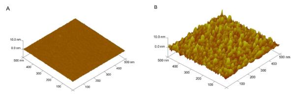
AFM topographical image (500 × 500 nm) of the OTCE fabricated with a single (A) or 12 layers (B) of protein adsorbed/pyrolyzed.
As it can be observed, the OTCE obtained with a single layer of protein adsorbed/pyrolyzed produced a thin and discontinued layer. On the contrary, the surface of the OTCE fabricated with 12 layers shows full coverage and abundant density of nanostructures. The surface roughness calculated by AFM was ± 0.7 nm. This value is in agreement with other thin electrodes fabricated with pyrolyzed photoresist (0.5 nm42, 0.8 nm20, 0.2 nm33), graphene (2 nm43), or indium-tin oxide (14 nm44).
Transmittance, Resistance, and Thickness
In order to take advantage of the proposed electrodes and rationally select the most suitable ones for a given application, the proper balance between transmittance and resistance should be achieved. This relationship is typically controlled by the thickness of the films. Therefore, the transparency of the films was evaluated in the 300 – 800 nm range and analyzed as a function of the number of layers of protein adsorbed/pyrolyzed. As it can be observed in Figure 2A, rather featureless spectra were obtained for all the substrates, showing only a slight decrease in transmittance as the wavelength decreases. Figure 2B shows a summary of the overall trend observed using 600 nm as the reference point. As it can be observed, and although the overall transmittance of the substrates was influenced by the number of layers of protein adsorbed/pyrolyzed, all electrodes were able to transmit at least 89% of the incident power, confirming the transparent nature of the films.
Figure 2.
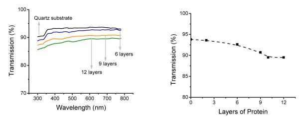
A: Representative transmission spectra of a series of OTCE on quartz.
B: Transparency of the proposed OTCE as a function of the number of layers of protein adsorbed/pyrolyzed.
In order to complement the transmission data, the resistance of the proposed OTCE was investigated as a function of the number of layers of protein adsorbed/pyrolyzed. Experiments were performed by measuring the resistance of the film between two gold contacts with a standard multi-meter (2-point probe). Based on the results presented in Figure 3A, electrodes were classified into three main groups. The first group, that included electrodes fabricated by adsorption/pyrolysis of 1-4 layers of protein, were not able to conduct electricity. These electrodes were not considered appropriate for the development of biosensors and therefore were not further investigated. The second group included electrodes fabricated with 5-9 layers of protein adsorbed/pyrolyzed and showed a proportional decrease in the film resistance. Similar trends have been reported for other OTCE as well as for metallic and semiconductor films.20 The third group of electrodes (fabricated by the adsorption/pyrolysis of ≥ 10 layers of protein) displayed a resistance lower than 1 kΩ·cm−1.
Figure 3.
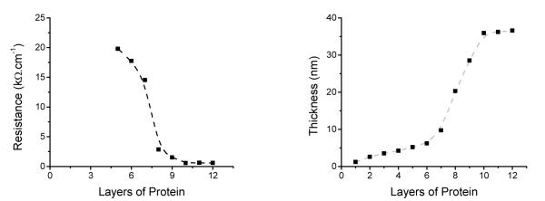
A. Resistance of OTCE as function of the number of layers of protein adsorbed/pyrolyzed. Each data point represents the average ± standard deviation obtained for three electrodes, independently prepared. Line included to guide the eye.
B. Thickness of OTCE as function of the number of layers of protein adsorbed/pyrolyzed as measured by AFM. Each data point represents the average ± standard deviation obtained for three electrodes, independently prepared. Line included to guide the eye.
As it determines the resistivity and the transparency of the OTCE,20 one of the most important parameters to control during the development of OTCE is the thickness of the deposited layer. For that reason, the evolution of the thickness as a function of the number of layers of protein adsorbed/pyrolyzed was determined by atomic force microscopy (AFM). As it can be observed in Figure 3B, significant increases in the thickness of the OTCE were observed as the number of layers of protein adsorbed/pyrolyzed increased from 1.2 ± 0.1 nm (1 layer) to 36.6 ± 0.3 nm (12 layers).
Electrochemical and Spectroscopic Characterization
In order to identify the most suitable electrodes for the potential development of biosensors, cyclic voltammetry experiments were performed. Initially, the limits of the OTCE under normal operational conditions were determined in supporting electrolyte using the electrode with the lowest resistance (fabricated with 12 layers of protein adsorbed/pyrolyzed). Under these conditions, no significant O2 or H2 evolution were observed within −0.5 V and 1.2 V. In agreement with result obtained with other OTCE,30 upon deoxygenation of the solution (bubbling N2 for at least 10 min) the onset for oxygen reduction was shifted to approximately −1.5 V (see Supporting Information). Next, the evolution of the electrochemical properties of the OTCE was investigated by CV, as a function of the number of layers of protein adsorbed/pyrolyzed and using 1.0 mM K3Fe(CN)6 (prepared in 0.1 M NaH2PO4/Na2HPO4 buffer + 0.1 M KCl, pH = 7.4) as the redox couple. Although electrodes fabricated with 1 – 4 layers of protein did not render oxidation/reduction peaks, one anodic current peak during the positive scan and the corresponding reduction peak in the negative sweep were observed for most of the other electrodes. As a summary of the results obtained, Figure 4 shows the dependence of the anodic and cathodic peak current (Ip, A) and peak potential (Ep, B) as a function of the number of layers of protein adsorbed/pyrolyzed used to fabricate the corresponding electrode.
Figure 4.
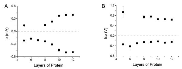
Summary of the peak current (A) and peak potential (B) as a function of the number of layers of protein adsorbed/pyrolyzed. Conditions: 1.0 mM K3Fe(CN)6 in 0.1 M NaH2PO4/Na2HPO4 buffer + 0.1 M KCl, pH = 7.4, scan rate: 100 mV·s−1. Each data point represents the average ± standard deviation obtained for three electrodes, independently prepared. Positive and negative values correspond to the anodic and cathodic process, respectively.
In agreement with the results described in Figure 3 (A and B), thicker electrodes (fabricated with more layers of protein adsorbed/pyrolyzed) yielded significantly larger oxidation/reduction peaks and smaller differences between the anodic and cathodic peak potentials (ΔEp). The ratio of the anodic and cathodic peak current was always lower than 0.94 and despite the gradual decreases, the difference between the anodic and cathodic peak potentials (ΔEp) was, in all cases, larger than 0.88 V (both values obtained for the electrode fabricated with 12 layers of protein adsorbed/pyrolyzed). These observations suggest that the resistance of the electrodes is responsible for the irreversible behavior observed. Similar results have been reported for similar systems.20, 45
The reproducibility of the proposed method was evaluated by evaluating the peak current (either anodic or cathodic wave) obtained for three electrodes, independently prepared. In all cases, the relative standard deviation of the peak current observed was lower than 5%. This finding was considered a mayor advantage of the proposed electrodes with respect to other carbon-based nanomaterials, which generally display poor batch-to-batch reproducibility.17-18
Based on these results and the fact that films with large internal resistances could induce variations in the applied potential distribution across the electrode surface and distort the electrochemical response, it was concluded that electrodes prepared with 12 layers of protein adsorbed/pyrolyzed were more suitable for the development of sensors and were further characterized. Although it could be possible to further improve the properties of the OTCE by adsorption/pyrolysis of more than 12 layers of BSA, such strategy would further expand the time required to prepare the electrodes and was not considered advantageous. Consequently, the influence of the scan rate was investigated in the 0.005 – 0.3 V/s range and using electrochemical couples of either negative (K3Fe(CN)6) or positive charge (Ru(NH3)6Cl3). Figure 5 shows representative voltammograms obtained for the selected couples at different sweep rates using OTCE fabricated with 12 layers of protein adsorbed/pyrolyzed.
Figure 5.
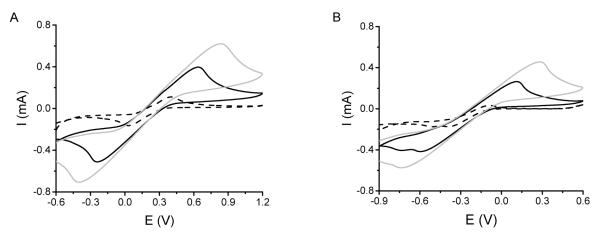
Potentiodynamic I/E profiles for 1.0 mM K3Fe(CN)6 (A) or 1.0 mM Ru(NH3)6Cl3 (B) obtained at 5 mV·s−1 (------), 100 mV·s−1 (——), and 300 mV·s−1 ( ). Conditions: 0.1 M NaH2PO4/Na2HPO4 buffer + 0.1 M KCl, pH = 7.4, OTCE fabricated with 12 layers of protein adsorbed/pyrolyzed.
At all scan rates, one anodic current peak during the positive scan and the corresponding reduction peak in the negative sweep were observed. The peak current showed a linear dependence with respect to the square root of the scan rate. In addition, significant shifts in the ΔEp were observed as the sweep rate increased (see Supporting Information). These observations suggest that although the reaction is a diffusion-controlled process and that no adsorption occurs at the interface, electrodes fabricated with 12 layers of proteins adsorbed/pyrolyzed exhibit some limitations, most likely due to the resistance of the film (IR drop). Complementary experiments conducted with both electrochemical couples but under different pH values (0.1 M NaH2PO4/Na2HPO4 buffer + 0.1 M KCl, pH = 6.4, 7.4, 8.4, or 11.4) did not yield to significant differences in either peak current or peak potential, indicating negligible electrostatic interactions between the electrochemical couples and the electrode surface.
In order to measure not only the internal resistance but also the charge-transfer resistance of the OTCE fabricated with 12 layers of protein adsorbed/pyrolyzed, electrochemical impedance spectra were collected. Figure 6 shows a representative example of a Nyquist plot obtained for these electrodes.
Figure 6.
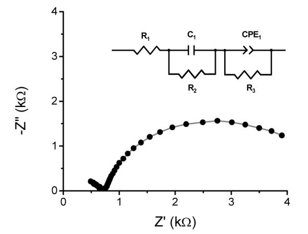
Nyquist plot obtained with an OTCE fabricated with 12 layers of protein adsorbed/pyrolyzed (•). Conditions: 1.0 mM K3Fe(CN)6 in 0.1 M NaH2PO4/Na2HPO4 buffer + 0.1 M KCl, pH = 7.4. Also included in the figure is the spectrum ( ) simulated with the proposed equivalent circuit (insert).
In order to obtain the assumed parameters on the proposed equivalent circuit, the spectrum was simulated using the equivalent circuit included in Figure 6 (see insert), where R1, kΩ = 0.35 ± 0.01, R2, kΩ = 0.36 ± 0.01, and R3, kΩ = 4.1 ± 0.1 and correspond to the resistance of the solution, the internal resistance of the film, and the charge-transfer resistance, respectively. Besides including an element to account for the capacitance of the film (C1, nF = 6.9 ± 0.6), the circuit also features a constant phase element (CPE1, μF = 6.7 ± 0.2) with an exponent constant (α = 0.83 ± 0.01) instead of the traditional Cdl (representing the capacitance of the double layer). In agreement with previous reports,46 this small change (pure capacitors display α = 1) yields better fittings of the model Nyquist plots to the experimental data by accounting for heterogeneities and roughness of the surface of the electrode (also evident in the AFM image). Similar circuits have been previously described in literature to represent CNT-modified electrodes.47-48 The quality of the fitting was evaluated using a built-in function in the software (chi-squared = 0.0081), which was considered adequate. The difference between these values and those obtained under DC conditions (2-point multimeter), suggests that the OTCE show the typical frequency dependence observed in other thin films.49-50
Raman spectroscopy was used to assess the structure of the electrodes fabricated with 12 layers of protein adsorbed/pyrolyzed. Figure 7 shows a representative Raman spectra corresponding to an OTCE and a silicon wafer, used as substrate. Although the underlying substrate does not have any remarkable signal, the OTCE displayed two intense features at 1360 cm−1 and 1605 cm−1. These peaks, also known as the D and E2g bands, are characteristic of carbon substrates and are associated with symmetry breakdown and sp2 lattices of graphitic structures, respectively.51 Although the position and intensity of these bands can be slightly affected by the temperature of the pyrolysis step52 or the presence of adsorbed oxygenated species,34 the ratio D/E2g can be typically used to obtain qualitative information related to the structural disorder of the carbon substrate.20, 34, 53 In order to obtain such information, the spectra shown in Figure 7 was deconvoluted into two Gaussian peaks (centered at the D and E2g bands) with areas of 55706 and 44320 counts·cm−1, respectively (R2 = 0.97). The D/E2g ratio of the areas of these bands was calculated to be 1.26. This value which is slightly higher than previously reported ratios for other OTCE fabricated from photoresists33 and traditional glassy carbon electrodes,36, 51 and could explain the resistive behavior observed by electrochemical impedance spectroscopy (see Figure 6), driving the irreversible electrochemical response (see Figure 4 and Figure 5). Although a-priori this may represent a disadvantage of the proposed OTCE with respect to traditional electrodes, the larger disorder and proportion of edges of the proposed OTCE could enable the fabrication of nanostructured electrodes with significantly higher electrochemical activity54 and density of functional groups on the surface.
Figure 7.
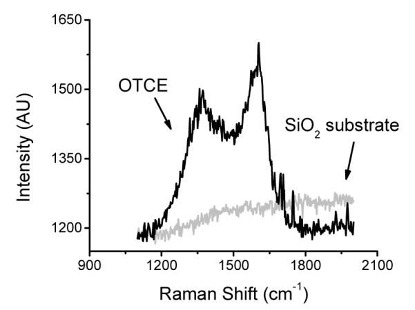
Raman spectra obtained with a plain wafer ( ) and an OTCE fabricated with 12 layers of protein adsorbed/pyrolyzed (—).
As previously stated, the optical constants of the OTCE were determined by ellipsometry by fitting a parameterized model to the measured data. In order to improve the accuracy of the calculation, the thickness of the substrate coated with 12 layers (obtained by AFM) and the optical properties of arc-evaporated carbon55 were used as the starting values for the fitting process. The results of the calculation, which display Kramers–Kronig consistency, are summarized in Figure 8. As it can be observed, an intense peak in k, attributed to the resonance of excitons in the carbon structure, was observed at 450 nm. Unlike structured carbon-based nanomaterials,37, 56 where strong and well-defined features are often observed (band gap at ~220 nm for crystalline diamond), the proposed OTCE displayed broader features, approaching those obtained with disordered carbon structures.36, 57
Figure 8.
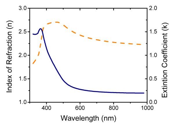
Dependence of the index of refraction (n, ——) and extinction coefficient (k, - - -) as a fucntion of the wavelength and as determined by ellipsometry for a OTCE fabricated with 12 layers of protein adsorbed/pyrolized.
OTCE-Based Biosensor
In order to demonstrate the potential applications of the described OTCE, the electrode fabricated with 12 layers of protein adsorbed/pyrolyzed was used to develop an amperometric sensor for glucose. The sensor was prepared following a previously described procedure4-5, 58-60 by immersing, for 1 hour under mild agitation, the OTCE in a solution containing 4 mg·mL−1 glucose oxidase (a model enzyme for bioanalytical applications) in 10 mM acetate buffer, matching the isoelectric point of the protein. The response of the sensor was evaluated by following the oxidation of H2O2 (produced by the oxidation of glucose) upon the sequential addition of glucose to a beaker containing 20 mL of 0.1 M NaH2PO4/Na2HPO4 buffer + 0.1 M KCl, pH = 7.4. The detection was performed in a three-electrode cell by applying at 0.8 V (vs Ag/AgCl/KClSAT). Figure 9 shows a typical calibration plot for glucose obtained with the GOx-modified OTCE, in the 1-100 mM range. At it can be observed, a linear least-squares fitting, calculated over the 1 – 10 mM concentration range, yielded a sensitivity and a limit of detection (3 times the noise value of the baseline) of 3.0 ± 0.1 nA·mM−1 and 10μM, respectively. The average response time was 14 ± 2 s.
Figure 9.
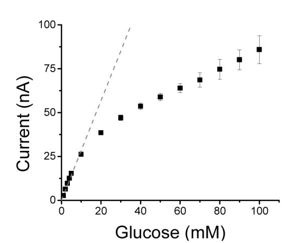
Calibration curve obtained with a OTCE fabricated with 12 layers of protein adsorbed/pyrolyzed and modified with GOx. Conditions: 0.1 M NaH2PO4/Na2HPO4 buffer + 0.1 M KCl, pH = 7.4, EDET = 0.8 V. Line represents the linear fitting obtained in the 1-10 mM range. Each data point corresponds to the average ± standard deviation obtained with 3 consecutive injections.
4. Conclusions
A series of optically-transparent carbon electrodes were developed by pyrolysis of adsorbed proteins. As most proteins interact with most surfaces, the process does not require specialized instrumentation and can be used to coat substrates of different composition, size, and shape. By sequential cycles of adsorption/pyrolysis, thicker layers of carbon can be produced. Although electrodes fabricated with 5-9 layers of protein showed moderate resistivity, films with < 1 kΩ·cm−1 can be systematically (RSD < 5%) produced by the deposition of 10 – 12 layers of protein. Substrates fabricated with 12 layers of protein adsorbed/pyrolyzed were able to facilitate electron-transfer reactions with irreversible behavior, likely associated with the internal resistance of the film. According to the presented results, the substrates display the characteristic Raman features of graphitic samples, with a large ratio of edges/basal (sp2) planes, therefore suggesting the presence of a significant number of sites that can be manipulated through standard chemical derivatization. In addition, the substrates display a high contact angle and a large density of nanostructures on the surface. The described substrates were used to develop a glucose biosensor with a performance that is comparable to other sensors recently published. All things considered, the presented methodology display advantages with respect to other procedures to fabricate transparent electrodes as it allows the fabrication of a novel carbon-based nanomaterial, with high uniformity, in almost any laboratory setting, and at a very low cost.
Supplementary Material
5. Acknowledgements
Financial support for this project has been provided in part by the University of Texas at San Antonio and the National Institutes of Health through the National Institute of General Medical Sciences (1SC3GM081085, 2SC3GM081085) and the Research Centers at Minority Institutions (G12MD007591). S. Alharthi thanks the scholarship provided by the Ministry of Higher Education of Saudi Arabia. Authors also thank Dr. P. Calvo for his help acquiring the Raman spectra and Dr. K. Chumbimuni-Torres for initial discussions related to the project.
Footnotes
6. Conflict of Interest Disclosure Authors declare no competing financial interest.
7. References
- 1.Murray RW. Nanoparticles: An Emerged and Lasting Frontier. Anal. Chem. 2009;81(5):1723–1723. doi: 10.1021/ac900238p. [DOI] [PubMed] [Google Scholar]
- 2.Liu H, Webster TJ. Nanomedicine for implants: A review of studies and necessary experimental tools. Biomaterials. 2007;28(2):354–369. doi: 10.1016/j.biomaterials.2006.08.049. [DOI] [PubMed] [Google Scholar]
- 3.Mora MF, Giacomelli CE, Garcia CD. Interaction of D-Amino Acid Oxidase to Carbon Nanotubes: Implications in the Design of Biosensors. Anal. Chem. 2009;81:1016–1022. doi: 10.1021/ac802068n. [DOI] [PMC free article] [PubMed] [Google Scholar]
- 4.Felhofer JL, Caranto J, Garcia CD. Adsorption Kinetics of Catalase to Thin Films of Carbon Nanotubes. Langmuir. 2010;26:17178–17183. doi: 10.1021/la103035n. [DOI] [PMC free article] [PubMed] [Google Scholar]
- 5.Khan R, Gorski W, Garcia CD. Nanomolar Detection of L-Glutamate Using Screen-Printed Electrodes Containing Multi-Wall Carbon Nanotubes. Electroanalysis. 2011;23:2357–2363. doi: 10.1002/elan.201100348. [DOI] [PMC free article] [PubMed] [Google Scholar]
- 6.Scida K, Stege PW, Haby G, Messina GA, Garcia CD. Recent Applications of Carbon-Based Nanomaterials to Analytical Chemistry: A Critical Review. Anal. Chim. Acta. 2011;691:6–17. doi: 10.1016/j.aca.2011.02.025. [DOI] [PMC free article] [PubMed] [Google Scholar]
- 7.Valcarcel M, Cardenas S, Simonet BM, Moliner-Martinez Y, Lucena R. Carbon nanostructures as sorbent materials in analytical processes. TrAC, Trends Anal. Chem. 2008;27(1):34–43. [Google Scholar]
- 8.Rivas GA, Rubianes MD, Rodríguez MC, Ferreyra NF, Luque GL, Pedano ML, Miscoria SA, Parrado C. Carbon nanotubes for electrochemical biosensing. Talanta. 2007;74(3):291–307. doi: 10.1016/j.talanta.2007.10.013. [DOI] [PubMed] [Google Scholar]
- 9.Jacobs CB, Peairs MJ, Venton BJ. Review: Carbon nanotube based electrochemical sensors for biomolecules. Anal. Chim. Acta. 2010;662(2):105–127. doi: 10.1016/j.aca.2010.01.009. [DOI] [PubMed] [Google Scholar]
- 10.Barnes TM, van de Lagemaat J, Levi D, Rumbles G, Coutts TJ, Weeks CL, Britz DA, Levitsky I, Peltola J, Glatkowski P. Optical characterization of highly conductive single-wall carbon-nanotube transparent electrodes. Phys. Rev. B. 2007;75(23):23541001–2354110. [Google Scholar]
- 11.Schrage C, Kaskel S. Flexible and Transparent SWCNT Electrodes for Alternating Current Electroluminescence Devices. ACS Applied Materials & Interfaces. 2009;1(8):1640–1644. doi: 10.1021/am9002588. [DOI] [PubMed] [Google Scholar]
- 12.Wang R, Sun J, Gao L, Zhang J. Base and Acid Treatment of SWCNT-RNA Transparent Conductive Films. ACS Nano. 2010;4(8):4890–4896. doi: 10.1021/nn101208m. [DOI] [PubMed] [Google Scholar]
- 13.Shim D, Jung S-H, Han SY, Shin K, Lee K-H, Han JH. Improvement of SWCNT transparent conductive films via transition metal doping. Chem. Comm. 2011;47(18):5202–5204. doi: 10.1039/c1cc10190k. [DOI] [PubMed] [Google Scholar]
- 14.Garoz-Ruiz J, Palmero S, Ibañez D, Heras A, Colina A. Press-transfer optically transparent electrodes fabricated from commercial single-walled carbon nanotubes. Electrochem. Comm. 2012;25:1–4. (0) [Google Scholar]
- 15.Han JT, Kim JS, Jo SB, Kim SH, Kim JS, Kang B, Jeong HJ, Jeong SY, Lee G-W, Cho K. Graphene oxide as a multi-functional p-dopant of transparent singlewalled carbon nanotube films for optoelectronic devices. Nanoscale. 2012;4(24):7735–7742. doi: 10.1039/c2nr31923c. [DOI] [PubMed] [Google Scholar]
- 16.Edgeworth JP, Wilson NR, Macpherson JV. Controlled Growth and Characterization of Two-Dimensional Single-Walled Carbon-Nanotube Networks for Electrical Applications. Small. 2007;3(5):860–870. doi: 10.1002/smll.200700029. [DOI] [PubMed] [Google Scholar]
- 17.Fam DWH, Palaniappan A, Tok AIY, Liedberg B, Moochhala SM. A review on technological aspects influencing commercialization of carbon nanotube sensors. Sens. Actuators, B. 2011;157(1):1–7. [Google Scholar]
- 18.Batzill M. The surface science of graphene: Metal interfaces, CVD synthesis, nanoribbons, chemical modifications, and defects. Surf. Sci. Rep. 2012;67(3–4):83–115. [Google Scholar]
- 19.Dai Y, Swain GM, Porter MD, Zak, Jerzy New Horizons in Spectroelectrochemical Measurements: Optically Transparent Carbon Electrodes. Anal. Chem. 2008;80(1):14–22. doi: 10.1021/ac085996r. [DOI] [PubMed] [Google Scholar]
- 20.Donner S, Li H-W, Yeung ES, Porter MD. Fabrication of Optically Transparent Carbon Electrodes by the Pyrolysis of Photoresist Films: Approach to Single-Molecule Spectroelectrochemistry. Anal. Chem. 2006;78(8):2816–2822. doi: 10.1021/ac052244d. [DOI] [PubMed] [Google Scholar]
- 21.Kummer M, Kirchhoff JR. Electron-transfer properties of pyrolytic graphite optically transparent electrodes. Electroanalysis. 1996;8(6):524–528. [Google Scholar]
- 22.Mattson JS, Smith CA. Optically transparent carbon film electrodes for infrared spectroelectrochemistry. Anal. Chem. 1975;47(7):1122–1125. [Google Scholar]
- 23.Matsuo Y, Iwasa K, Sugie Y, Mineshige A, Usami H. Preparation of carbon-based transparent and conductive thin films by pyrolysis of silylated graphite oxides. Carbon. 2010;48(14):4009–4014. [Google Scholar]
- 24.Walker EK, Vanden Bout DA, Stevenson KJ. Carbon Optically Transparent Electrodes for Electrogenerated Chemiluminescence. Langmuir. 2011;28(2):1604–1610. doi: 10.1021/la2042394. [DOI] [PubMed] [Google Scholar]
- 25.Singh A, Jayaram J, Madou M, Akbar S. Pyrolysis of Negative Photoresists to Fabricate Carbon Structures for Microelectromechanical Systems and Electrochemical Applications. J. Electrochem. Soc. 2002;149(3):E78–E83. [Google Scholar]
- 26.Anjo DM, Brown S, Wang L. Performance evaluation of an easily prepared optically transparent carbon film electrode. Anal. Chem. 1993;65(3):317–319. doi: 10.1021/ac00051a022. [DOI] [PubMed] [Google Scholar]
- 27.Rodriguez AT, Li X, Wang J, Steen WA, Fan H. Facile Synthesis of Nanostructured Carbon through Self-Assembly between Block Copolymers and Carbohydrates. Adv. Funct. Mat. 2007;17(15):2710–2716. [Google Scholar]
- 28.Burckel DB, Washburn CM, Raub AK, Brueck SRJ, Wheeler DR, Brozik SM, Polsky R. Lithographically Defined Porous Carbon Electrodes. Small. 2009;5(24):2792–2796. doi: 10.1002/smll.200901084. [DOI] [PubMed] [Google Scholar]
- 29.Siegal MP, Overmyer DL, Provencio PP, Tallant DR. Linear Behavior of Carbon Nanotube Diameters with Growth Temperature. J. Phys. Chem. C. 2010;114(35):14864–14867. [Google Scholar]
- 30.DeAngelis TP, Hurst RW, Yacynych AM, Mark HB, Heineman WR, Mattson JS. Carbon and mercury-carbon optically transparent electrodes. Anal. Chem. 1977;49(9):1395–1398. [Google Scholar]
- 31.Valenti LE, Fiorito PA, Garcia CD, Giacomelli CE. The adsorption-desorption process of bovine serum albumin on carbon nanotubes. J. Colloid Interface Sci. 2007;307(2):349–356. doi: 10.1016/j.jcis.2006.11.046. [DOI] [PubMed] [Google Scholar]
- 32.Chumbimuni-Torres KY, Coronado RE, Mfuh AM, Castro-Guerrero C, Silva MF, Negrete GR, Bizios R, Garcia CD. Adsorption of Proteins to Thin-Films of PDMS and Its Effect on the Adhesion of Human Endothelial Cells. RSC Advances. 2011;(4):706–714. doi: 10.1039/C1RA00198A. [DOI] [PMC free article] [PubMed] [Google Scholar]
- 33.Lee H, Rajagopalan R, Robinson J, Pantano CG. Processing and Characterization of Ultrathin Carbon Coatings on Glass. ACS Appl. Mater. Interfaces. 2009;1(4):927–933. doi: 10.1021/am900032p. [DOI] [PubMed] [Google Scholar]
- 34.Kostecki R, Schnyder B, Alliata D, Song X, Kinoshita K, Kötz R. Surface studies of carbon films from pyrolyzed photoresist. Thin Solid Films. 2001;396(1-2):36–43. [Google Scholar]
- 35.Crooks RD, Ioana, Yancey, David Dual-Elctrode Microfluidic Cell for Characterizing Electrocatalysts. Lab Chip. 2011:47. doi: 10.1039/c2lc21181e. [DOI] [PubMed] [Google Scholar]
- 36.McCreery RL. Advanced Carbon Electrode Materials for Molecular Electrochemistry. Chem. Rev. 2008;108(7):2646–2687. doi: 10.1021/cr068076m. [DOI] [PubMed] [Google Scholar]
- 37.Soetedjo H, Mora MF, Garcia CD. Optical properties of single-wall carbon nanotube films deposited on Si/SiO2 wafers. Thin Solid Films. 2010;518(14):3954–3959. doi: 10.1016/j.tsf.2010.02.037. [DOI] [PMC free article] [PubMed] [Google Scholar]
- 38.Wehmeyer J, Bizios R, Garcia CD. Adsorption of Bovine Serum Albumin to Nanostructured Thin-Films of TiO2. Mat. Sci. Eng. C. 2010;30(2):277–282. doi: 10.1016/j.msec.2009.11.002. [DOI] [PMC free article] [PubMed] [Google Scholar]
- 39.Alterovitz SA, Johs B. Multiple minima in the ellipsometric error function. Thin Solid Films. 1998;313-314:124–127. [Google Scholar]
- 40.Shrestha RP, Yang D, Irene EA. Ellipsometry study of poly(o-methoxyaniline) thin films. Thin Solid Films. 2006;500(1-2):252–258. [Google Scholar]
- 41.Larsericsdotter H, Oscarsson S, Buijs J. Structure, stability, and orientation of BSA adsorbed to silica. J. Colloid Interface Sci. 2005;289(1):26–35. doi: 10.1016/j.jcis.2005.03.064. [DOI] [PubMed] [Google Scholar]
- 42.Ranganathan S, McCreery RL. Electroanalytical Performance of Carbon Films with Near-Atomic Flatness. Anal. Chem. 2001;73(5):893–900. doi: 10.1021/ac0007534. [DOI] [PubMed] [Google Scholar]
- 43.Weber CM, Eisele DM, Rabe JP, Liang Y, Feng X, Zhi L, Müllen K, Lyon JL, Williams R, Bout DAV, Stevenson KJ. Graphene-Based Optically Transparent Electrodes for Spectroelectrochemistry in the UV–Vis Region. Small. 2010;6(2):184–189. doi: 10.1002/smll.200901448. [DOI] [PubMed] [Google Scholar]
- 44.Purica M, Iacomi F, Baban C, Prepelita P, Apetroaei N, Mardare D, Luca D. Investigation of structural properties of ITO thin films deposited on different substrates. Thin Solid Films. 2007;515(24):8674–8678. [Google Scholar]
- 45.Niwa D, Takano N, Yamada T, Osaka T. Nickel electroless deposition process on chemically pretreated Si(100) wafers in aqueous alkaline solution. Electrochim. Acta. 2003;48(9):1295–1300. [Google Scholar]
- 46.Szroeder P. Electron transfer kinetics at single-walled carbon nanotube paper: The role of band structure. Physica E Low Dimens Syst Nanostruct. 2011;44(2):470–475. [Google Scholar]
- 47.Diakowski PM, Xiao Y, Petryk MWP, Kraatz H-B. Impedance Based Detection of Chemical Warfare Agent Mimics Using Ferrocene-Lysine Modified Carbon Nanotubes. Anal. Chem. 2010;82(8):3191–3197. doi: 10.1021/ac902694d. [DOI] [PubMed] [Google Scholar]
- 48.Basuray S, Senapati S, Aijian A, Mahon AR, Chang H-C. Shear and AC Field Enhanced Carbon Nanotube Impedance Assay for Rapid, Sensitive, and Mismatch-Discriminating DNA Hybridization. ACS Nano. 2009;3(7):1823–1830. doi: 10.1021/nn9004632. [DOI] [PubMed] [Google Scholar]
- 49.McIntyre JF, Leidheiser H. Resistance measurements on thin-film substrates as a technique for studying the deterioration of coated metals. Ind. Eng. Chem. Prod. R. D. 1985;24(3):348–353. [Google Scholar]
- 50.Barrau S, Demont P, Peigney A, Laurent C, Lacabanne C. DC and AC Conductivity of Carbon Nanotubes–Polyepoxy Composites. Macromolecules. 2003;36(14):5187–5194. [Google Scholar]
- 51.Wang Y, Alsmeyer DC, McCreery RL. Raman spectroscopy of carbon materials: structural basis of observed spectra. Chem. Mater. 1990;2(5):557–563. [Google Scholar]
- 52.Everall NJ, Lumsdon J, Christopher DJ. The effect of laser-induced heating upon the vibrational raman spectra of graphites and carbon fibres. Carbon. 1991;29(2):133–137. [Google Scholar]
- 53.Koenig F. T. a. J. L. Raman Spectrum of Graphite. J. Chem. Phys. 1970;53:1126. [Google Scholar]
- 54.Banks CE, Davies TJ, Wildgoose GG, Compton RG. Electrocatalysis at graphite and carbon nanotube modified electrodes: edge-plane sites and tube ends are the reactive sites. Chem. Commun. 2005;7:829–841. doi: 10.1039/b413177k. [DOI] [PubMed] [Google Scholar]
- 55.Palik ED. Handbook of Optical Constants of Solids. Academic Press; New York, NY: 1997. [Google Scholar]
- 56.Weber JW, Calado VE, van de Sanden MCM. Optical constants of graphene measured by spectroscopic ellipsometry. Appl Phys Lett. 2010;97(9):091904. [Google Scholar]
- 57.Lee J, Collins RW, Veerasamy VS, Robertson J. Analysis of the ellipsometric spectra of amorphous carbon thin films for evaluation of the sp3-bonded carbon content. Diamond Relat. Mater. 1998;7(7):999–1009. [Google Scholar]
- 58.Nejadnik MR, Francis L, Garcia CD. Nanoscale Scaffolds of Carbon Nanotubes for Immobilization of Glucose Oxidase. Electroanalysis. 2011;23(6):1462–1469. doi: 10.1002/elan.201000758. [DOI] [PMC free article] [PubMed] [Google Scholar]
- 59.Nejadnik MR, Garcia CD. Staining proteins: A simple method to increase the sensitivity of ellipsometric measurements in adsorption studies. Colloids Surf. B. 2011;82(1):253–257. doi: 10.1016/j.colsurfb.2010.08.021. [DOI] [PMC free article] [PubMed] [Google Scholar]
- 60.Cabral MF, Barrios JD, Kataoka EM, Machado SAS, Carrilho E, Garcia CD, Ayon AA. Computational, electrochemical, and spectroscopic, studies of acetycholinesterase covalently attached to carbon nanotubes. Colloids Surf. B. 2013;103(1):624–629. doi: 10.1016/j.colsurfb.2012.08.039. [DOI] [PubMed] [Google Scholar]
Associated Data
This section collects any data citations, data availability statements, or supplementary materials included in this article.


