

Abstract
High-bandwidth and low-noise nanopore sensor and detection electronics are crucial in achieving single-DNA base resolution. A potential way to accomplish this goal is to integrate solid-state nanopores within a CMOS platform, in close proximity to the biasing electrodes and custom-designed amplifier electronics. Here we report the integration of solid-state nanopore devices in a commercial complementary metal-oxide semiconductor (CMOS) potentiostat chip implemented in On-Semiconductor’s 0.5 μm technology. Nanopore membranes incorporating electrodes are fabricated by post-CMOS micromachining utilizing the N+ polysilicon/SiO2/N+ polysilicon capacitor structure available in the aforementioned process. Nanopores are created in the CMOS process by drilling in a transmission electron microscope and shrinking by atomic layer deposition. We also describe a batch fabrication method to process a large of number of electrode-embedded nanopores with sub-10 nm diameter across CMOS-compatible wafers by electron beam lithography and atomic layer deposition. The CMOS-compatibility of our fabrication process is verified by testing the electrical functionality of on-chip circuitry. We observe high current leakage with the CMOS nanopore devices due to the ionic diffusion through the SiO2 membrane. To prevent this leakage, we coat the membrane with Al2O3 which acts as an efficient diffusion barrier against alkali ions. The resulting nanopore devices also exhibit higher robustness and lower 1/f noise as compared to SiO2 and SiNx. Furthermore, we propose a theoretical model for our low-capacitance CMOS nanopore devices, showing good agreement with the experimental value. In addition, experiments and theoretical models of translocation studies are presented using 48.5 kbp λ-DNA in order to prove the functionality of on-chip pores coated with Al2O3.
1. Introduction
Genes, proteins and other biomolecules provide a wealth of information that is essential for the diagnosis and treatment of diseases. One of the key bottlenecks to the widespread use of personalized medicine is the lack of a low-cost, high-throughput, accurate and easy-to-use biomolecule detection platform. The realization of such a detection platform will also aid in the early detection of disease, which in cases such as cancer greatly enhance the survival rate. Fundamentally, sensing results in a binary response to the presence or absence of a particular target. Nature accomplishes this complex task, with exquisite precision, by utilizing channels or pores combined with molecular recognition. The mechanism often involves the gating of ion fluxes though nanometer sized molecular pores or channels. This change in ion flux then regulates other pathways either directly or via secondary pathways.
Recently, inspired by biology, nanopores have emerged as a possible single-molecule electronic detection platform [1–3]. A nanopore is an extremely tiny hole, few nanometers in diameter, in an insulating membrane that separates two ionic reservoirs. An applied voltage across the nanopore results in an ionic current that flows through the nanopore. The principle of single-molecule detection using the nanopore is based on detecting the blockage of this ionic current by the target. The first application of nanopores to biosensing was performed using a biological pore, α-Hemolysin, for the possible sequencing of DNA. Initially, it was hoped that molecular size and nature of functional groups of each nucleobase will result in an appreciable change in ionic current as the DNA threads through the nanopore [4]. Unfortunately, though some ionic current changes were observed, they were not due to the single nucleobase differences but rather due to folding and stacking effects [5]. Since then there has been intense activity, in both academia and industry, towards realizing a single-molecule detector based on the nanopore and many excellent reviews are available [1–3]. Recent advances include solid-state nanopores [1], biological pores modified with molecular adapters [6] and single base detectors that couple exonuclease activity and the nanopore [7].
One of the primary reasons for such a vigorous effort in the field of nanopore sensors is their promise of realizing fast, cheap, reliable and label-free sensors, especially for DNA sequencing. Compared to existing methods of DNA sequencing that require several thousands of dollars and many weeks to complete a sequence [8], nanopores have the potential to reduce the time to a few days at a significantly lower cost, though many challenges are to be overcome. One of the primary challenges that have been identified is the integration of the nanopore platform and potentiostat electronics [1]. A potentiostat enables the application of a fixed potential across the membrane and measures the current going through the nanopore. An efficient integrated platform will reduce the parasitic capacitance; enable a wider bandwidth and a lower noise operation, which can greatly enhance the sensitivity of the nanopore. Recently, it has been demonstated that by simply placing an integrated potentiostat chip close to a separate nanopore chip vastly larger bandwidths could be achieved [9]. We believe this can be further enhanced by coupling the circuit and the nanopore more intimately. Additionally by coupling the nanoscale sensor and the sensing electronics closed-loop feedback can be implemented that can increase the dynamic range of the sensor. Furthermore due to the batch-fabrication nature of IC processes, massively-parallel sensors with integrated electronics can be built. This is a crucial step if on-chip sequencing or massively parallel biosensing is to become a reality.
This paper reports on the fabrication and characterization of integrated solid state nanopore devices in a standard complementary metal-oxide-semiconductor (CMOS) potentiostat chip. Each step in the fabrication process was carefully optimized to ensure compatibility with the CMOS process. This is validated by the electrical characterization of the on-chip CMOS circuitry after every process step. In addition, the low complexity of the proposed process results in high device yield. The bulk properties of the membrane were studied by transmission electron microscopy (TEM), energy dispersive x-ray spectroscopy (EDX), and electron energy loss spectroscopy (EELS). We also present a method to batch process a large of number of identical nanopore devices across large CMOS-compatible wafers by electron beam lithography (EBL). The integrity of both CMOS and CMOS-compatible nanopore devices is demonstrated by measuring the conductance, capacitance and noise characteristics. The functionality of these nanopores in the CMOS chip was also demonstrated through the detection of 48.5 kbp double-stranded λ-DNA in 1M KCl under an applied electric field.
2. Fabrication and characterization
2.1 Fabrication of oxide membrane in CMOS
Our custom-designed CMOS potentiostat chip is 1.7 mm × 1.7 mm × 260 μm, implemented in On-Semiconductor’s C5N 0.5 μm technology (figure 1(a)). This technology is a low-cost, non-silicided CMOS process facilitating stacked contacts with three metal layers and two highly n-doped polysilicon layers. Figure 2(a) shows a schematic cross-section of the CMOS circuitry in On-Semiconductor’s 0.5 μm process. To make highly sensitive nanopore devices, we have utilized the polysilicon-insulator-polysilicon (PIP) structure available in this process [10]. Doped polysilicon layers, having thickness of 370 nm and 250 nm, in this capacitor are used as biasing electrodes across the nanopore. The insulator sandwiched between the polysilicon layers is a thin (35nm) silicon dioxide layer where the synthetic membrane containing pore is fabricated. PIP capacitor is chosen over other types of capacitors such as metal-insulator-metal (MIM) capacitor, because insulators in PIP capacitors are deposited by sophisticated chemical vapor deposition (CVD) techniques such as low pressure chemical vapor deposition (LPCVD), and they are of higher quality [11]. On the other hand, insulators in MIM capacitors are usually deposited by plasma enhanced chemical vapor deposition (PECVD). PECVD insulators are more prone to defects or pinholes. As a result, they are lower quality insulators. In addition, polysilicon layers in PIP are more mechanically robust and show better chemical resistance as compared to the metal layers of MIM [11]. Inset of figure 1(a) shows an expanded image of the PIP capacitor. The size of the bottom polysilicon (Poly 1) and top polysilicon (Poly 2) layers are 150 μm × 150 μm and 15 μm × 15 μm, respectively. An SEM cross-section of the PIP capacitor along AB direction (as indicated in inset of figure 1(a)) is given in figure 1(b). Inset of figure 1(b) clearly shows different layers of PIP capacitor with the underlying field oxide (FOX) and silicon substrate.
Figure 1.

(a) Optical micrograph of the CMOS potentiostat chip implemented in On-semiconductor’s 0.5 μm technology. Inset shows an expanded image of the PIP capacitor that is utilized to fabricate nanopore devices and electrodes. (b) SEM cross-section of the PIP capacitor along AB direction as indicated in inset of (a). Inset shows a magnified view of the capacitor, FOX and substrate.
Figure 2.

(a) Cross-sectional schematic of a CMOS integrated chip implemented in On-semiconductor’s 0.5 μm process. (b) Cross-sectional representation of the same technology after the fabrication of nanopore devices and electrodes utilizing PIP capacitor in close proximity to the CMOS amplifier circuitry. (c) Process flow to create oxide membranes and electrodes in PIP capacitor. (i) Passivate the backside of chip with PECVD Si3N4. (ii) Pattern a 5 μm × 5 μm window on the frontside and etch the oxynitride passivation. (iii) Open a 100 μm × 100 μm window on the backside. Etch nitride passivation by ICP and silicon substrate by DRIE. (iv) Remove FOX by ICP etch. (v) Deposit Al2O3 by ALD on the backside for the isolation of bulk substrate. (vi) Etch Al2O3 under the poly 1 layer by ICP. (vii) Create membranes and electrodes by removing polysilicon layers by XeF2 etch.
Nanopore devices with adjacent electrodes were fabricated in the CMOS chip by applying post-CMOS micromachining (figure 2(b)). First the custom-designed CMOS potentiostat chips were fabricated via the Metal-Oxide-Semiconductor Implementation Service (MOSIS). The process flow to fabricate oxide membranes in CMOS chips is given in figure 2(c). For simplicity, only the PIP capacitor portion of the chip is included in this flow. The process starts with the deposition of a 500 nm thick Si3N4 passivation by PECVD on the backside of CMOS chip (figure 2(c).i). A 5 μm square window was then lithographically patterned on the frontside of chip. The pattern was transferred to the oxynitride passivation (thickness, ~5 μm) by inductively coupled plasma etch (ICP) (CHF3 flow rate 20 sccm, ICP power 900 W, RF power 200 W, chamber pressure 0.5 Pa) (figure 2(c).ii). The chip was then flipped and a 100 μm square window was patterned on the backside. Nitride passivation at the bottom was removed by ICP etch using the aforementioned process conditions. This was followed by the anisotropic etching of silicon substrate by deep reactive ion etch (DRIE) using FOX as etch-stop (figure 2(c).iii). After that, the FOX layer was etched in ICP (figure 2(c).iv). A 100 nm Al2O3 film was then deposited by atomic layer deposition (ALD) on the backside of the chip to isolate the bulk silicon substrate from the ionic solution and prevent a short electrical path during the subsequent electrochemical characterization of nanopore devices (figure 2(c).v). A short ICP etch anisotropically removed Al2O3 that was deposited underneath the polysilicon 1 layer (figure 2(c).vi). In the final step, a free-standing oxide membrane was created by etching the polysilicon layers in XeF2 (figure 2(c).vii). Figures 3(a) and 3(b) show the SEM micrographs of top and cross-section of a fabricated SiO2 membrane in CMOS chip. The thickness of the membrane obtained from SEM was 35nm. This thickness was also confirmed by measuring electron energy loss spectrum (EELS) of the membrane by employing an FEI Titan FEG TEM with Gatan Enfina EELS spectrometer at an accelerating voltage of 300 kV (Figure 3c). The thickness of membrane is obtained from the log-ratio method [12] using the following expression.
Figure 3.

(a) SEM top-view of a free-standing SiO2 membrane fabricated in CMOS chip. (b) SEM cross-section of the same membrane with thickness, ~35 nm. (c) EELS results of membrane which were used to calculate the membrane thickness by applying the log-ratio method. The ZLP in the spectrum is scaled by a factor of 0.03, relative to the rest of the spectrum. (d) EDX spectrum of the membrane illustrating the presence of Si and O, and their composition.
| (1) |
Where λ is the mean-free path of inelastic electron scattering in oxide, I is the integrated intensity under the total EEL spectrum and I0 is the integrated intensity under the zero loss peak (ZLP). The thickness calculated from this method is 37.8 nm which is close to the value from SEM. In addition, Energy-dispersive X-ray spectroscopy (EDX) was performed to determine the elemental composition of the membrane. Figure 3(d) shows the EDX spectrum recorded from the oxide membrane in CMOS chip. Strong peaks were observed in the EDX spectrum at X-ray energies that are characteristic of silicon and oxygen. Compositional analysis revealed 31% Si and 69% O, which is in good agreement with the expected stoichiometric film ratio of 33.33% Si and 66.67% O.
2.2 Post-fabrication characterization of CMOS
The post-CMOS micromachining process of a CMOS chip needs to be carefully planned and implemented so that the process is non-destructive to on-chip circuitry. There are various factors that need to be considered in post-CMOS micromachining. 1) Process steps must be compatible with the existing materials in the chip. 2) Adhesion of any deposited material on the exposed surface of the chip needs to be carefully evaluated with due consideration to process compatibility. 3) Post-CMOS micromachining imposes a strict thermal budget (< 450°C), due to the degradation of on-chip metal layers above this temperature [13]. Additionally, high temperature can result in cracks due to the mismatch of thermal expansion coefficients of films. 4) Plasma processes used for the deposition and etching of materials can cause breakdown or degradation of gate dielectric in transistors due to the plasma induced charge accumulation in the dielectric [14]. 5) Owing to the small size, the chip needs to be handled carefully to prevent breakage and contamination. Due to the large number of constraints imposed, it is important to verify that the performance of CMOS circuitry is unchanged between each fabrication step.
To verify that our process is CMOS-compatible, electrical measurements were performed on a supply independent current source circuit already present on the CMOS potentiostat chip. The reason this circuit serves as an ideal process indicator is that the bias voltages are directly proportional to process parameters which is reflected in the unified parameter of threshold voltage [15]. Threshold variations can cause functional failures, slower operating speeds or reduced dynamic range. A schematic of the supply independent current source is given in figure 4.
Figure 4.
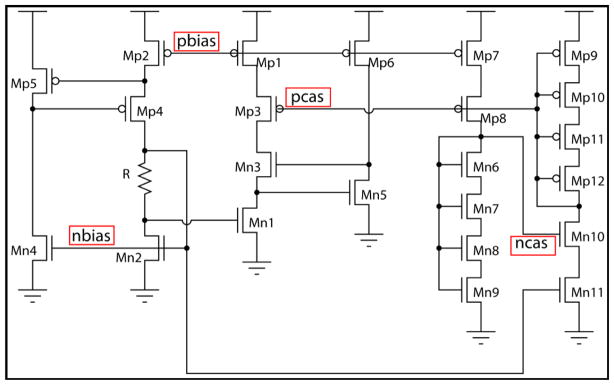
Supply independent current source circuit of the CMOS chip. The circuit was utilized to test the functionality of CMOS circuitry after every post-CMOS micromachining step.
Table 1 list the voltage values at critical nodes of the circuit labeled as pbias, pcas, ncas and nbias, measured on an unprocessed die and a processed die after every fabrication step. The measured voltages on the unprocessed and processed chips match very well. This proves that our fabrication process does not have any detrimental effect on the CMOS circuitry.
Table 1.
Test results of processed and unprocessed dies at Vdd = 5V.
| pbias (V) | pcas (V) | ncas (V) | nbias (V) | ||
|---|---|---|---|---|---|
| Unprocessed Chip | 3.655 | 3.200 | 1.847 | 1.396 | |
| Fabrication step | |||||
| Processed Chip | After frontside ICP etch of oxynitride | 3.637 | 3.186 | 1.852 | 1.406 |
| After backside Bosch etch of Si | 3.633 | 3.174 | 1.836 | 1.378 | |
| After backside ICP etch of FOX | 3.639 | 3.184 | 1.848 | 1.399 | |
| After XeF2 etch of poly-layers | 3.645 | 3.183 | 1.857 | 1.403 | |
2.3 Reliability of CMOS membrane
To investigate the reliability of fabricated membranes in CMOS chip, we measured ionic conductance through membranes containing no pores. Figure 5(a) shows the experimental setup used for this experiment (Methods). The CMOS chip was mounted between cis and trans reservoirs filled with solution, 1 M KCl 10 mM TRIS-HCl buffer 1mM EDTA at pH 8. Using Ag/AgCl electrodes and a potentiostat, a voltage was applied across the membrane and the resulting ionic current was measured.
Figure 5.
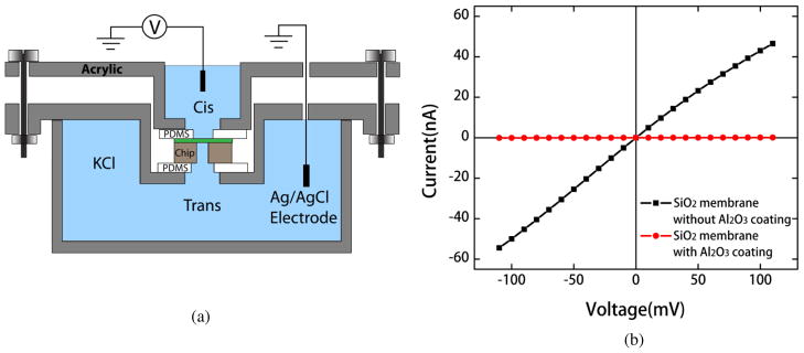
(a) Schematic cross-section of the experimental setup. The CMOS chip containing the membrane was mounted between cis and trans reservoirs filled with aqueous buffer solution. A patch-clamp current amplifier was used to apply bias across the membrane and measure ionic current. (b) Current-voltage characteristics of a CMOS SiO2 membrane at 1M KCl before (black line) and after (red line) the deposition of Al2O3 by ALD. Very large conductance was measured with the blank oxide membrane due to the drift of K+ ions through SiO2 under applied electric field. Ionic leakage was eliminated by coating the membrane with Al2O3.
The current-voltage (I-V) characteristics of the blank CMOS membrane were obtained by sweeping the applied potential from −100 mV to 100 mV (figure 5(b), black curve). The current measured with the blank membrane is exceedingly large at all voltages. This large current is a result of the ionic current leakage through the membrane. Since SiO2 is a relatively low-density (2.2 g/cm3) material, K+ ions in the buffer solution can drift through it easily under the influence of an electric field [16]. Similar drift phenomenon of alkali ions through gate oxide was previously reported to cause a shift in threshold voltage and introduce instabilities in the operation of Metal-Oxide-Semiconductor Field Effect Transistor [17]. To prevent ion diffusion through membrane, we chose to coat the membrane with a high-density insulator that acts a good diffusion barrier against K+ ions. ALD is the preferred method for the uniform coating of dielectrics because it can produce homogeneous films with precise thickness control due to self-limiting growth mechanisms [18]. It is also a low-temperature process (100°–300°C) which makes it compatible with CMOS process. Other deposition techniques such as LPCVD lack sub-nanometer precision over film thickness and the elevated deposition temperature (600–800°C) is not compatible with CMOS process [19]. Silicon nitride acts as an efficient barrier to mobile ions due to its high density (~3.1 g/cm3) [20]. But the deposition of SiNx by ALD is a challenge because of the preferential reaction of ALD precursors with the oxygen containing species [21]. Hence we opted for a different insulator such as Al2O3 that exhibits negligible ion diffusion, and can be deposited by ALD. Al2O3 was previously used to develop low-noise and high-throughput nanopore devices [22, 23].
A 30nm thick layer of Al2O3 was deposited by ALD (Methods) on the CMOS membrane and ionic conductance through the membrane was measured again. Figure 5(b) (red curve) shows the I-V characteristics of the Al2O3-coated membrane. Clearly, Al2O3 coating results in negligible current through the membrane, due to the blockage of mobile ions. Non-zero conductance was measured through the membrane due to the capacitive coupling between measuring electrodes. However, this background conductance is 2 or 3 orders of magnitude smaller than the expected conductance of a nanopore. We also explored the long-term reliability of the Al2O3-coated CMOS membrane by measuring the conductance through the membrane at regular intervals over an extended period. Conductance values were found to remain stable even after 12-hour period. This validates the chemical and mechanical stability of Al2O3 coated membrane in electrolyte solution.
2.4 Fabrication of CMOS nanopores
Nanopores with relatively large diameter were directly drilled in the SiO2 membranes of CMOS chip using a tightly focused electron beam in a FEI Titan field-emission-gun TEM at 300 kV. Al2O3 was then deposited by ALD on the membrane to reduce the size of pores to sub-10nm. The TEM drilling technique in combination with the ALD Al2O3 shrinkage allows for robust membranes containing finely tuned pores in CMOS chip. Figures 6(a) and 6(b) show the TEM images of a 60 nm SiO2 pore drilled by TEM, and the corresponding Fast Fourier Transform (FFT) which confirms the amorphous structure of the pore. The size of this pore was subsequently decreased to 5×7 nm by ALD Al2O3 (figure 6(c)). Bright diffraction spots were clearly visible in the corresponding FFT (figure 6(d)), indicating the crystalline nature of the Al2O3-coated pore.
Figure 6.
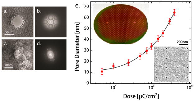
(a) TEM image of a 60 nm CMOS oxide pore that was directlyirectly drilled by TEM. (b) Corresponding FFT showing the amorphous structure of of SiO2 pore. (c) TEM image of the same pore (~5×7 nm) after the deposition of Al2O3 by ALD. (d) Corresponding FFT indicating the poly-crystalline nature of Al2O3 coated pore. (e) EBL fabricated pore diameter as a function of e-beam dose on a CMOS-compatible wafer. The top left corner shows a picture of a fully-processed 4-inch CMOS-compatible wafer containing 19 × 19 membrane chips. SEM image of an array of ~25 nm pores fabricated by EBL is given in the bottom right corner.
2.5 CMOS compatible wafer-scale nanopores
Wafer-scale processing is an important part of fabricating nanostructures in a cost-effective way. To enable wafer-scale processing, we investigated pore fabrication by electron beam lithography (EBL) as an alternative to TEM drilling. First, we determined process parameters such as etch times for different materials and nanofabrication of pores in separate CMOS-compatible wafers prepared using the same process conditions as CMOS chip (Methods). This enables the tuning of process parameters on relatively inexpensive wafers rather than on fully processed CMOS chips. Nanopores with diameters, ~10 – 70 nm were then fabricated in the CMOS-compatible membranes across 4-inch wafers by EBL with e-beam exposure doses ranging from 5×10³ to 4×10⁵ μC/cm2 followed by ICP etch (Methods). Figure 6(e) plots the resulting pore diameter as a function of applied e-beam dose (red symbol). The pore diameter shows a monotonic dependence on the e-beam dose. This trend can be described by the simple equation, dpore = α.Dβ with α ≈ 4.76 nm/(μC/cm2), β ≈ 0.43 and (figure 6(e), black line). The SEM image of an array of EBL-fabricated pores with diameter ~25 nm is also shown in figure 6(e). A close inspection of 25 nm pores across the wafer revealed variations of ±3 nm in pore diameter. This deviation could be a result of the slight variations in the membrane thickness across the wafer. Unlike TEM drilling technique which suffers from low process throughput, the EBL method allows for the production of a large number of identical pores within a single processing batch. However, it is difficult to fabricate sub-10 nm features by EBL process due to limiting factors such as e-beam scattering [24], resist chemistry [25], and critical dimension loss during pattern transfer [26]. We compensated for this limitation by applying ALD process and obtained sub-10 nm pores across the CMOS-compatible wafer. Furthermore, the EBL process used to fabricate these pores are CMOS-compatible and readily available in a commercial CMOS foundry enabling seamless transition to a standard CMOS process. In addition to the EBL approach, we also used these CMOS compatible wafers to process nanopores by the TEM method to enable measurement of conductance versus pore-diameter.
3 Experiments and modeling
3.1 Conductance, noise and capacitance
We measured the ionic conductance of pores in CMOS-compatible chips at high salt concentration. To find the theoretical conductance of pores, we used the geometrical models which assumed a double-conical shape [27, 28] and a hyperboloid [29] shape for nanopore, incorporating the access resistance outside the pore, as shown in inset of figure 7(a). These models are characterized by parameters such as total pore length, L, effective pore length, Leff, the narrowest diameter of pore, d, the widest diameter of pore, D, and electrolyte conductivity, σ. The access resistance (Ra = 1/2σd) is obtained by considering a planar disc at the pore entrance [30]. As demonstrated previously by Peng Chen et. al. [22], Al2O3-coating by ALD reduces the surface charge of nanopore to negligible values. This was further verified by the lack of anion selectivity of our pores as shown in figure 7(b) indicating minimal surface charge effects. Hence the effect of surface charges is neglected in these models and the pore conductance exhibits bulk behaviour.
Figure 7.

(a) Pore conductance of 10 non-CMOS pores and a CMOS pore (indicated by arrow) with diameters, 4 – 40 nm at 1M KCl. The hyperboloid model with D = d + 30 nm (black line) and the truncated double-cone model with Leff = 0 and α ≈14° (orange line) gave the best fit to the conductance of TEM-drilled pores. The EBL-fabricated pores were best described by the double-cone conductance model with Leff = 58 nm and α ≈ 71° (red line). (b) Current-voltage characteristics of a 5 × 7 nm CMOS pore measured in 0.01M, 0.1M and 1M KCl. (c) Power spectral densities of three different nanopores at 100 mV in 1M KCl. 1/f noise was significantly decreased with an Al2O3-coated CMOS pore as compared to a SiO2-coated CMOS pore and a commercially available nitride pore. (d) A lumped element circuit model of a simple nanopore device representing pore resistance, access resistance and membrane capacitance. A more accurate model for the CMOS nanopore chip is superimposed on the geometrical structure of the chip. The displacement current paths between the ionic reservoirs as indicated by 1 – 4 contribute to the total capacitance of the device.
Figure 7(a) shows the pore conductance vs. diameter characteristics at 1M KCl obtained from 10 different CMOS-compatible pores and a CMOS pore of varying diameters (4–40nm). Blue squares represent the TEM drilled pores whereas green circles indicate pores that are fabricated by EBL. To model the conductance of these pores, L and σ were considered to be 66 nm and 11.3 S/m (at 22°C). It was found that the conductance of TEM pores can best be described by the hyperboloid model (figure 7(a), black line). Applying a nonlinear regression fit to the experimental data, and assuming a linearly varying asymptotic angle α for the hyperbolic model (Supplementary data), an outer diameter of D ≈ d + 30 nm was extracted for the TEM drilled pores. This value is in line with the previous experimental studies reported on pore shape [27, 28, 31]. Alternatively, an equivalent fit (figure 7(a), orange line) could also be obtained using an end-to-end truncated double cone (i.e. Leff = 0) pore with an angle of α ≈14° (Supplementary data). Though this model is useful for simple geometrical calculations, the sharp edges do not represent the physical picture accurately compared to the hyperboloid model. On the other hand, the best fit to the conductance of EBL pores was obtained by applying the double-cone model (figure 7a, red line) with Leff ≈ 58 nm and α ≈71°. These extracted values suggest that while describing the EBL nanopores the double-cone model almost transforms to a model which assumes a cylindrical shape for the pore. This can be explained by the fact that EBL pores are most likely to possess a cylindrical structure since they are defined by the anistropic ICP etch. The small difference in L and Leff probably resulted from the slight horizontal etch at the pore entrance during ICP process. We also performed the conductance measurements of a CMOS nanopore with diameter, 5 × 7 nm at three different KCl concentrations. I-V characteristics of this pore are given in figure 7b. The slight non-linear I-V behavior could arise from the asymmetric pore geometry and inhomogeneous surface charge distribution [32, 33]. As expected, the conductance of pore scales with the increasing concentration of KCl.
In addition, the noise characteristics of on-chip nanopores were studied. In the low-frequency regime (<100 Hz), noise is dominated by flicker noise arising from fluctuations in the pore’s ionic conductance [34]. Figure 7c shows the power spectrum density of current noise at an applied voltage of 100 mV from two CMOS pores with diameter, ~5 nm. CMOS Pore 1 is coated with 30 nm ALD Al2O3 whereas CMOS pore 2 is covered with 25 nm ALD Al2O3 and 3 nm ALD SiO2. For comparison, we have also included the noise spectrum measured with a similar-size pore in a commercially available (Norcada, Inc.) 50 μm × 50 μm SiNx membrane with thickness, 30 nm. Pore 1 shows 2–3 orders of magnitude improvement in low-frequency 1/f noise as compared to other two pores. It has been noted previously that the mobility fluctuation model, via the Hooge parameter, best describes 1/f noise in nanopores [34]. This conclusion was based on experimental evidence that the noise is proportional to the density rather than the square of the density as predicted by the surface trap based number fluctuation model. An alternative view is that surface state scattering induced mobility fluctuation could also lead to the observed behavior [35]. An ALD coated Al2O3 pore shows significantly decreased 1/f noise compared to an ALD coated SiO2 pore and an uncoated SiNx pore indicating a substantial reduction in surface charged states. The low surface charge exhibited by these pores substantiated by the bulk conductance and non-rectifying behavior further validates the view that charged surface states are reduced by ALD coated Al2O3. Thus the sensitivity of a CMOS integrated nanopore can be significantly enhanced by coating it with Al2O3.
At high frequencies (>10 kHz), the dominant noise source is the interaction of amplifier’s voltage noise with any parasitic capacitance at the amplifier input including the capacitance from the nanopore device. Hence it is important to minimize the capacitance of the nanopore chip. The capacitance of the CMOS nanopore chip is measured by employing a virtual lock-in amplifier embedded in Patchmaster software (HEKA Instruments Inc). Most surface of our CMOS chip was covered with a thick PDMS gasket, leaving only a small circular area (~diameter, 1 mm) exposed to the electrolyte. As a result, the membrane capacitance was reduced to ~7.8 pF. We also modeled the capacitance of the CMOS nanopore chip. In its simplest form, a nanopore device is modeled as a pore resistance, Rp, in series with an access resistance, Ra, along with the membrane capacitance, Cm (figure 7(d)). A more accurate model can be developed for the CMOS chip by recognizing different displacement current paths (labeled as 1, 2, 3 and 4 shown in figure 7(d)) between the ionic reservoirs, and calculating the capacitance due to each path by applying the simple expression for capacitance to each layer of material on the chip. Then the total capacitance of the device is obtained by adding all parallel capacitances (CTotal = C1+C2+C3+C4) (Supplementary data). From this model, the total capacitance computed was ~6.68 pF. This modeled capacitance shows good agreement with the experimentally measured value. The small discrepancy between the theoretical prediction and the experimental result is probably due to the parasitic capacitance resulting from the capacitive coupling between the electrolyte solution and a small part of the CMOS circuitry exposed to it.
3.2 Translocation of DNA molecules
The functionality of on-chip nanopores is demonstrated by performing the translocation studies of λ-DNA. Unmethylated 48.5 kbp double-stranded λ-DNA (length, LDNA ~ 16 μm) was commercially purchased (New England BioLabs, Inc.). With a negative potential at the cis reservoir, a stable open pore conductance was established through I-V sweeps and control current measurements prior to the introduction of DNA molecules. No current blockades were observed in absence of DNA molecules. The molecules were then added to the cis reservoir at a concentration between 100 and 500 ng/μL. Considering a persistence length, lp of 50 nm, λ-DNA is expected to adopt a highly coiled conformation at high-salt concentration with a radius of gyration, . Once captured by the pore, DNA molecules stretch and traverse the pore. We detected events indicating the translocation of DNA utilizing the previously described CMOS pore. Figure 8(a) plots the ionic current versus time trace at −400 mV before and after the addition of 48.5 kbp λ-DNA. Both linear and folded events were observed in the trace, which is consistent with the translocation studies reported before [36, 37]. A few typical events are shown in the bottom panel of figure 8(a). Translocations events were defined as those that decreased the open pore current to more than three times the standard deviation of the open pore current. Current depressions with durations less than the electrical response of the system (~60 μs) were excluded from the analysis. The event parameters, peak conductance blockage ratio, and the dwell time, td were calculated by analyzing the recorded current trace. The baseline for the current trace was determined by using a moving average over a 50 ms period. Figure 8(b) shows a scatter plot of and td of a number of 3215 events, where each point represents a single translocating event. The histogram plots of these parameters are also included in figures 8(c) and 8(d). The histogram of can be fitted by the sum of three Gaussian curves as evidenced by three peaks labeled as I, II and III. The truncation of the Gaussian curve I results from the exclusion of events below a threshold value as defined above. We interpret that the Gaussian curves are caused either by the interaction of DNA with pore or by the presence of single or multiple double strands of the passing DNA inside the pore. Curve I corresponds to shallow blockades indicating interrogation of dsDNA with the pore, curve II represents linear translocation events, and curve III corresponds to deeper blockade events due to single or higher order folding of dsDNA. As seen from figure 8c, the predominant events are located at a value of ~7%.
Figure 8.

(a) Measured ionic current versus time at −400 mV using a CMOS nanopore with diameter, 5 × 7 nm. The blockades in the current are due to the translocation of 48.5 kbp λ-DNA molecules. The bottom panel shows three typical events at an increased time resolution. (b) Scatter plot of 3215 events recorded. For each event the dwell time and the peak blockage ratio were determined. Each point in the graph corresponds to a single event. (c) Histogram of observed peak blockage ratio for 48.5 kbp DNA molecules. (d) Histogram of observed dwell times for 48.5 kbp DNA.
To theoretically predict , we calculated the change in ionic conductance, ΔG through pore due to the presence of λ-DNA. The hyperboloid model of conductance was employed to determine ΔG since this model provided the best fit to the conductance of TEM nanopores as discussed before. In addition, the DNA molecule was assumed to have a hyperboloid shape. Based on these geometrical considerations, we can obtain ΔG from the following equations [29].
| (2) |
| (3) |
where dpore, deff and dDNA are the open pore diameter, the effective pore diameter (with DNA inside the pore), and the thinnest diameter of the hyperboloid dsDNA; ra and rb are the major and minor lengths of the elliptical cross-section of pore. Taking dDNA = 2.2 nm, ra = 7 nm and rb = 5 nm, ΔG calculated from this model was ~1.33 nS. This yields a blockage ratio of 7.65% (Supplementary data). We also obtained a similar result (~7.14%) for by applying the truncated double-cone conductance model with a linear cylindrically shaped DNA inserted coaxially as shown in top right inset of figure 8(c). Based on this model, the following expressions were used to calculate Br.
| (4) |
| (5) |
| (6) |
| (7) |
| (8) |
Where, da1 and da2 are the effective diameters at the entrance and the narrow part of cone, hpore is the length of a truncated cone, RTrCone is the effective resistance of a truncated cone and Geff is the total effective conductance of the double cone including access resistance, Ra. Both these models match remarkably well with the experimental value. This indicates that the majority of events are unfolded events. To understand the origin of peak III at ~10% in the histogram, we examined event traces that correspond to this peak blockage ratio. These traces exhibited two distinct levels of blockades indicating an unfolded strand followed by a folded strand. To model these events, we used the analytically tractable double-cone model with a partially-folded cylindrical DNA inside the cone (Supplementary data). This model revealed that a of ~10% is obtained when the length of the folded part of DNA inside the double cone, hfold = hpore × 98% i.e. approximately half of the pore is occupied by folded DNA. Intuitively this makes sense since it would be expected that the small pore diameters used would unravel the DNA at the mouth of the pore. Additionally, the model predicts that events with ~7% blockage ratio are unfolded events. Since the average conductance blockage ratio, obtained from the translocation experiment was also ~7% (Supplementary data), the majority of the events are most probably unfolded events which is atypical of such pores and might be due to the inert surface offered by Al2O3 in our pores. The distribution of td values is best approximated by a monotonically decreasing exponential function. The average dwell time, found from analysis was ~200 μs. Storm et. al. [38] have observed a mean dwell time of ~1 ms for DNA of the same length, under a proportionally smaller voltage bias (120 mV). It has also been shown that dwell times are directly proportional to bias voltage conditions. Applying the above scaling we should observe a of ~300 μs, which agrees reasonably well with our results.
4. Conclusions
This work presents the development of nanopore devices in close proximity with the electrodes and amplifier electronics in a foundry fabricated CMOS potentiostat chip implemented in On-Semiconductor’s 0.5 μm process. PIP capacitor in this process was utilized to fabricate oxide membranes containing pores, and polysilicon electrodes. On-chip CMOS circuitry was electrically measured after every fabrication step to confirm that the proposed fabrication process is compatible with CMOS. Nanopores were fabricated in the CMOS process by the combination of TEM drilling and ALD coating. Alternatively by using EBL and ALD process, we extended the process to batch fabrication of a large number of nanopore devices on a single CMOS-compatible wafer. However, the diffusion of K+ ions through the SiO2 membrane causes high leakage current. This leakage phenomenon was eliminated by coating the membrane with Al2O3 which blocks the diffusion of K+ ions. Al2O3 coating of pores also resulted in superior noise performance and increased life-time over other solid-state counterparts. A 2–3 orders of magnitude improvement in low-frequency noise was observed with Al2O3 coated CMOS nanopores as compared to SiO2 and SiNx nanopores. A theoretical model for the capacitance of CMOS nanopore device was also developed by considering different displacement current paths through the device between the ionic reservoirs. The modeled capacitance shows a good match with the low capacitance value experimentally measured with CMOS chips. In addition, the detection of 48.5 kbp λ-DNA using this new architecture was demonstrated with signal-to-noise ratio being on par with the state-of-the-art solid state nanopore technology. The CMOS integrated nanopore devices described here serves as a platform to implement next-generation nanopore detectors that will offer vastly wider bandwidth and lower noise. Such an integrated approach has the potential to discover new phenomena at the nanoscale governing biomolecule transport and yield a new class of massively parallel biosensors.
5.1 Methods
5.1 Wafer-scale CMOS-compatible pores by electron beam lithography
The fabrication process started with the depositon of field oxide, polysilicon 1, gate oxide and polysilicon 2 layers on a double-side polished 4-inch-diameter silicon (100) wafer using the process conditions of On-Semiconductor’s C5N 0.5 μm technology [10]. 500 nm thick Si3N4 passivation layers were deposited on both sides of wafer by PECVD. An array of 19 × 19 free-standing membranes spaced 4.6 mm apart, were created in this structure across the wafer following the same process flow as previously described with CMOS chip. The wafer containing membranes was then spin-coated with e-beam resist, ZEP-520A (thickness, ~80 nm) and baked on hotplate at 180°C for 5 min. EBL was used to pattern circular pores in a JEOL JBX-6300FS EBL system at 100 keV with doses ranging from 5×10³ to 4×10⁵ μC/cm2. Exposed ZEP was developed in 1:1 MIBK: IPA for 60 s and rinsed in 9:1 MIBK: IPA for 30 s at 22°C. Pattern of pores were then transferred to oxide membranes by ICP etch (CHF3/O2 flow rate 45/5 sccm, ICP power 500 W, RF power 100 W, chamber pressure 0.5 Pa, etch time 40s).
5.2 Atomic layer deposition
Atomic layer deposition of Al2O3 was performed in FlexAL system (Oxford Instruments). Before placement in the ALD system, all samples were exposed to UV/ozone for 10 min to generate reactive hydroxylated surfaces. Trimethylaluminum [Al(CH3)3] (Sigma-Aldrich Co.) and O2 plasma were used as precursor and oxygen source for the film deposition. One reaction cycle of ALD consists of the following steps. (1) Flow precursor for 1 s, (2) Purge Ar for 5 s, (3) O2 plasma (RF 150W) for 5 s, and (4) Purge Ar for 5s. The substrate temperature was 300°C. The deposition rate of Al2O3 obtained using this process was 1.15 Å/cycle.
5.3 Nanopore setup
The CMOS chip containing the membrane was horizontally clamped between two acrylic fluidic chambers (Figure 5a). Poly(dimethylsiloxane) (PDMS) gaskets were used to achieve watertight seal between chip and fluidic compartments. The chip separates two fluidic chambers where the top and bottom chambers contain 80 μL and 15 mL of electrolyte solution. Before placing the chip in the experimental setup, the chip was cleaned in Piranha at 80°C for 10 minutes followed by an exposure to O2 plasma for a minute. This process removes organic contaminants and renders a thin oxide layer on the surface, enhancing the wettability of pores [37]. Immediately after the O2 exposure, the reservoirs were filled with salt solution, 1 M KCl 10 mM TRIS-HCl buffer 1mM EDTA at pH 8. The salt solution was prepared using 18 M Ω Milli-Q filtered water (Millipore). Ag/AgCl electrodes were placed in reservoirs for electrical contact to solution. The entire set-up was placed in a Faraday cage to minimize electrical noise pick-up. A patch-clamp amplifier and head-stage, EPC10 (HEKA Instruments) was used to apply a transmembrane voltage and to detect and amplify the resulting ionic current. The amplified current signal was low-pass filtered at 17.2 kHz using a Bessel filter and digitized at 200 kHz. Data were analyzed using MATLAB (MathWorks) and Clampfit (Axon Instruments).
Supplementary Material
Acknowledgments
We would like to thank Derek Stein for advice on nanopore experiments, and MOSIS, especially Wes Hansford, for supporting chip fabrication. This research was supported in part by Intel Corporation under Grant SB090065, the National Institute of Health (NIH) through the NIH Director’s New Innovator Award Program 1-DP2-OD007472-01, and the National Science Foundation (NSF) CAREER Award, NSF-CAREER CBET-1056092.
References
- 1.Dekker C. Solid-state nanopores. Nat Nanotechnol. 2007;2:209–15. doi: 10.1038/nnano.2007.27. [DOI] [PubMed] [Google Scholar]
- 2.Branton D, et al. The potential and challenges of nanopore sequencing. Nat Biotechnol. 2008;26:1146–53. doi: 10.1038/nbt.1495. [DOI] [PMC free article] [PubMed] [Google Scholar]
- 3.Howorka S, Siwy Z. Nanopore analytics: sensing of single molecules. Chem Soc Rev. 2009;38:2360–2384. doi: 10.1039/b813796j. [DOI] [PubMed] [Google Scholar]
- 4.Kasianowicz JJ, Brandin E, Branton D, Deamer DW. Characterization of individual polynucleotide molecules using a membrane channel. Proc Natl Acad Sci USA. 1996;93:13770–3. doi: 10.1073/pnas.93.24.13770. [DOI] [PMC free article] [PubMed] [Google Scholar]
- 5.Akeson M, Branton D, Kasianowicz JJ, Brandin E, Deamer DW. Microsecond time-scale discrimination among polycytidylic acid, polyadenylic acid, and polyuridylic acid as homopolymers or as segments within single RNA molecules. Biophys J. 1999;77:3227–33. doi: 10.1016/S0006-3495(99)77153-5. [DOI] [PMC free article] [PubMed] [Google Scholar]
- 6.Astier Y, Braha O, Bayley H. Toward single molecule DNA sequencing: direct identification of ribonucleoside and deoxyribonucleoside 5′-monophosphates by using an engineered protein nanopore equipped with a molecular adapter. J Am Chem Soc. 2006;128:1705–10. doi: 10.1021/ja057123+. [DOI] [PubMed] [Google Scholar]
- 7.Clarke J, Wu H-C, Jayasinghe L, Patel A, Reid S, Bayley H. Continuous base identification for single-molecule nanopore DNA sequencing. Nat Nanotechnol. 2009;4:265–70. doi: 10.1038/nnano.2009.12. [DOI] [PubMed] [Google Scholar]
- 8.Pettersson E, Lundeberg J, Ahmadian A. Generations of sequencing technologies. Genomics. 2009;93:105–11. doi: 10.1016/j.ygeno.2008.10.003. [DOI] [PubMed] [Google Scholar]
- 9.Rosenstein JC, Wanunu M, Merchant CA, Drndic M, Shepard KL. Integrated nanopore sensing platform with sub-microsecond temporal resolution. Nat Meth. 2012;9:487–92. doi: 10.1038/nmeth.1932. [DOI] [PMC free article] [PubMed] [Google Scholar]
- 10.Towner JM, Naughton J, Prasad J. Polysilicon interface engineering for improved PIP capacitors. ECS Trans. 2007;6:153–66. [Google Scholar]
- 11.Singh R, Harame DL, Oprysko MM. Silicon germanium: technology, modeling, and design. John Wiley & Sons, Inc; NJ: 2004. [Google Scholar]
- 12.Iakoubovskii K, Mitsuishi K, Nakayama Y, Furuya K. Thickness measurements with electron energy loss spectroscopy. Microsc Res Tech. 2008;71:626–31. doi: 10.1002/jemt.20597. [DOI] [PubMed] [Google Scholar]
- 13.Takeuchi H, Wung A, Sun X, Howe RT, King T-J. Thermal budget limits of quarter-micron foundry CMOS for post-processing MEMS devices. IEEE Trans Electron Devices. 2005;52:2081–86. [Google Scholar]
- 14.Shin HC, Hu C. Thin gate oxide damage due to plasma processing. Semicond Sci Technol. 1996;11:463–73. [Google Scholar]
- 15.Uddin A, Milaninia K, Chen C-H, Theogarajan L. Wafer scale integration of CMOS chips for biomedical applications via self-aligned masking. IEEE Trans Compon Packag Manuf Technol. 2011;1:1996–2004. doi: 10.1109/TCPMT.2011.2166395. [DOI] [PMC free article] [PubMed] [Google Scholar]
- 16.Snow E, Grove A, Deal B, Sah C. Ion transport phenomena in insulating films. J Appl Phys. 1965;36:1664–73. [Google Scholar]
- 17.Kuhn M, Silversmith DJ. Ionic contamination and transport of mobile ions in MOS structures. J Electrochem Soc. 1971;118:966–970. [Google Scholar]
- 18.Gordon RG, Hausmann D, Kim E, Shepard J. A kinetic model for step coverage by atomic layer deposition in narrow holes or trenches. Chem Vap Dep. 2003;9:73–8. [Google Scholar]
- 19.Madou M. Fundamentals of microfabrication. CRC Press; NY: 1997. [Google Scholar]
- 20.Osenbach J, Voris S. Sodium diffusion in plasma-deposited amorphous oxygen-doped silicon nitride (a-SiON: H) films. J Appl Phys. 1988;63:4494–4500. [Google Scholar]
- 21.Oxford Instruments. Available at: http://www.oxford-instruments.com/products/etching-deposition-growth/publications/process-news/january-2009/Pages/ultra-thin-silicon-nitride-films.aspx.
- 22.Chen P, Mitsui T, Farmer DB, Golovchenko J, Gordon RG, Branton D. Atomic layer deposition to fine-tune the surface properties and diameters of fabricated nanopores. Nano Lett. 2004;4:133–7. doi: 10.1021/nl0494001. [DOI] [PMC free article] [PubMed] [Google Scholar]
- 23.Venkatesan BM, Dorvel B, Yemenicioglu S, Watkins N, Petrov I, Bashir R. Highly sensitive, mechanically stable nanopore sensors for DNA analysis. Adv Mater. 2009;21:1–6. doi: 10.1002/adma.200803786. [DOI] [PMC free article] [PubMed] [Google Scholar]
- 24.Broers AN. Resolution limits of PMMA resist for exposure with 50 kV electrons. J Electrochem Soc. 1981;128:166–170. [Google Scholar]
- 25.Rooks MJ, Kratschmer E, Viswanathan R, Katine J, Fontana RE, MacDonald SA. Low stress development of poly (methylmethacrylate) for high aspect ratio structures. J Vac Sci Technol, B. 2002;20:2937–2941. [Google Scholar]
- 26.Wi JS, Lee HS, Lim K, Nam SW, Kim HM, Park SY, Lee JJ, Hong CD, Jin S, Kim KB. Fabrication of silicon nanopillar teradot arrays by electron-beam patterning for nanoimprint molds. Small. 2008;4:2118–2122. doi: 10.1002/smll.200800625. [DOI] [PubMed] [Google Scholar]
- 27.Kim MJ, Wanunu M, Bell C, Meller A. Rapid fabrication of uniformly sized nanopores and nanopore arrays for parallel DNA analysis. Adv Mater. 2006;18:3149–3153. [Google Scholar]
- 28.Kim MJ, McNally B, Murata K, Meller A. Characteristics of solid-state nanometer pores fabricated using a transmission electron microscope. Nanotechnology. 2007;20:205302. [Google Scholar]
- 29.Kowalcyzk SW, Grosberg AY, Rabin Y, Dekker C. Modeling the conductance and DNA blockade of solid-state nanopores. Nanotechnology. 2011;22:315101. doi: 10.1088/0957-4484/22/31/315101. [DOI] [PubMed] [Google Scholar]
- 30.Hall JE. Access resistance of a small circular pore. J Gen Physiol. 1975;66:531–2. doi: 10.1085/jgp.66.4.531. [DOI] [PMC free article] [PubMed] [Google Scholar]
- 31.Van den Hout M, Hall AR, Wu MY, Zandbergen HW, Dekker C, Dekker NH. Controlling nanopore size, shape and stability. Nanotechnology. 2010;21:115304. doi: 10.1088/0957-4484/21/11/115304. [DOI] [PubMed] [Google Scholar]
- 32.Hille B. Ion channels of excitable membranes. 3. Sinauer Associates; Sunderland, MA: 2001. [Google Scholar]
- 33.Siwy Z, Gu Y, Spohr HA, Baur D, Wolf-Reber A, Spohr R, Apel PY, Korchev YE. Rectification and voltage gating of ion currents in a nanofabricated pore. Europhys Lett. 2002;60:349–55. [Google Scholar]
- 34.Smeets RMM, Keyser UF, Dekker NH, Dekker C. Noise in solid-state nanopores. Proc Natl Acad Sci USA. 2008;105:417–21. doi: 10.1073/pnas.0705349105. [DOI] [PMC free article] [PubMed] [Google Scholar]
- 35.Hung KK, Ko PK, Hu C, Cheng YC. A unified model for the flicker noise in metal-oxide-semiconductor field-effect transistors 1990. IEEE Trans Electron Devices. 37:654–665. [Google Scholar]
- 36.Li J, Gershow M, Stein D, Brandin E, Golovchenko JA. DNA molecules and configurations in a solid-state nanopore microscope. Nat Mater. 2003;2:611–5. doi: 10.1038/nmat965. [DOI] [PubMed] [Google Scholar]
- 37.Storm AJ, Storm C, Chen JH, Zandbergen H, Joanny JF, Dekker C. Fast DNA translocation through a solid-state nanopore. Nano Lett. 2005;5:1193–7. doi: 10.1021/nl048030d. [DOI] [PubMed] [Google Scholar]
- 38.Storm AJ, Chen JH, Zandbergen HW, Dekker C. Translocation of double-strand DNA through a silicon oxide nanopore. Phys Rev E. 2005;71:051903. doi: 10.1103/PhysRevE.71.051903. [DOI] [PubMed] [Google Scholar]
Associated Data
This section collects any data citations, data availability statements, or supplementary materials included in this article.