Abstract
Solid-state nanopores can be fabricated in a variety of ways and form the basis for label-free sensing of single nanoparticles: as individual nanoparticles traverse the nanopore, they alter the ionic current across it in a characteristic way. Typically, nanopores are described by the diameter of their limiting aperture, and less attention has been paid to other, fabrication-dependent parameters. Here, we report a comprehensive analysis of the properties and sensing performance of three types of nanopore with identical 50nm aperture, but fabricated using three different techniques: direct ion beam milling, ion beam sculpting, and electron beam sculpting. The nanopores differ substantially in physical shape and chemical composition as identified by ion-beam assisted cross sectioning and energy dispersive x-ray spectroscopy. Concomitant differences in electrical sensing of single 30nm beads, such as variations in blockade depth, duration, and electric field dependence, are observed and modeled using hydrodynamic simulations. The excellent agreement between experiment and physical modeling shows that the physical properties (shape) and not the chemical surface composition determine the sensing performance of a solid-state nanopore in the absence of deliberate surface modification. Consequently, nanoparticle sensing performance can be accurately predicted once the full three dimensional structure of the nanopore is known.
Keywords: solid-state nanopore, nanopore geometry, characterization, ionic current, single nanoparticle detection
In 1953, the Coulter counter was invented for counting and sizing microscale particles dispersed in electrolytes.1-3 When a voltage is applied across a small opening that connects two chambers filled with electrolytes, particles are moved from one chamber to the other, and create characteristic resistive pulses (blockades) in the ionic current. In the 1990s, the Coulter counter principle was extended to the molecular level by introducing nanopores with limiting apertures ranging from ~1-200nm. Such nanopores are now widely used in numerous fields such as single molecule detection, molecule identification and DNA/RNA sequencing and protein detection.4-8
Today, nanopores consist of either funnel-shaped proteins9,10 or nanoscale openings in solid-state membranes.11,12 Compared to protein nanopores, solid-state nanopores have the advantages of mechanical robustness, reusability, tunable diameter, and stability in different physical and chemical environments. They also offer a wider choice of fabrication methods, including single shot (direct) ion beam milling, ion beam milling followed by reshaping the nanopore with additional ion or electron beam exposure, high energy electron beam milling, and chemical etching.13,14
Historically, the main focus in nanopore fabrication has been on the size of the limiting aperture, which determines the largest particle size that can move through the nanopore and strongly influences the amount of current reduction during a translocation event. Only recently has the influence of physical nanopore geometry started to receive more attention.15-17 Non-negligible effects on the translocation signals were found in large (200-300nm aperture) nanopores with small thickness-to-diameter aspect ratios.18 However, since the detection and analysis of small bioparticles (such as viruses, ribosomes, proteins, and nucleic acids) require significantly smaller and higher-aspect ratio nanopores, it is important to identify how the physical shape and chemical composition affect current sensing performance at these smaller length scales.
Here, we report a systematic investigation of these questions using three types of nanopores with identical aperture size (50nm), but fabricated using three of the most common methods: direct ion beam drilling (DD) and ion beam drilling followed by assisted shrinking using an ion beam (IBS) or electron beam (EBS). Both the chemical composition and the cross-sectional shapes of the nanopores are measured, revealing substantial fabrication-dependent differences. The effect of these factors on the sensing characteristics of each nanopore for translocation of 30nm nanobeads is determined, with comparison to parameter-free models built using commercial software. Having access to the detailed vertical width profile of each nanopore, we are able to show unambiguously the dominant influence of the physical shape of the nanopore on its electrical behavior.
Milling and resizing nanopores
In principle, focused ion beam (FIB) milling of nanopores is straightforward: a narrow ion beam is focused onto a thin membrane to sputter away material, leaving behind a small hole in the membrane.19-21 Unfortunately, the diameter of nanopores is difficult to control during the milling process and even nanopores fabricated under nominally identical conditions often vary from sample to sample because of small variations in ion beam condition, membrane irregularities, environmental noise, temperature, etc. As a result, several techniques to resize nanopores have been developed, commonly utilizing ion or electron beam irradiation.22-25 The mechanisms responsible for the resizing are varied and range from simple adatom migration26-28 to fluidization of the Si3N4 membrane24 to hydrocarbon deposition.25
Characterization
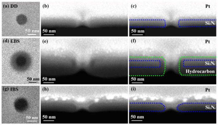
We milled and resized three types of nanopores using the methods of direct drilling, electron beam shrinking and ion beam shrinking. After resizing, we captured top-down images of each nanopore using the scanning electron microscope (Figures 1a, 1d, 1g), taking care to minimize any additional beam exposure.
Figure 1.
Scanning electron micrographs of nanopores. The left column shows top-down images of (a) directly drilled, (d) electron beam shrunk, and (g) ion beam shrunk nanopores. Images (a) and (g) were taken with 20kV electron beam, and image (d) was taken using 5kV electron beam to enhance contrast around the aperture. The middle column shows side views of the same nanopores after deposition of a protective top layer of platinum and cross-sectioning. The initially milled diameters were (b) 50nm, (e) 114nm and (h) 70nm, before resizing to identical 50nm apertures. In (c), (f) and (i), the shape of the nanopore before platinum deposition is outlined to aid the eye. All cross-section images were taken with a 5kV electron beam.
After all tests on nanopores were completed, they were cross-sectioned using the ion beam to obtain more detailed structural information. To protect the nanopores during the cross-sectioning process, a thin platinum layer was deposited using the electron beam and a gas injection system.29 Figures 1b, 1e and 1h show the resulting cross-sections. While previous studies generally assume that nanopores are right circular cylinders,30,31 TEM cross-section images by Kuan et al. demonstrated that nanopores can deviate from that ideal in a variety of ways, depending on fabrication method.17 Our cross-section images also show deviation from the right circular cylinder, although the deviation differs from that presented by Kuan et al. While we cannot conclusively identify the source of this difference, the use of different equipment and fabrication conditions could easily account for it.
As shown in Figure 1, our directly drilled nanopores have a mostly cylindrical shape, with the expected 50nm diameter and 50nm length, but exhibit rounded edges on the top and the bottom. Electron beam shrunk nanopores have similar shape, but their length is markedly increased (about 130 nm in the example shown in Figure 1). Finally, the shape of ion beam shrunk nanopores differs significantly and is closer to that of a double cone, with a wider opening on the top and a narrower opening on the bottom. We note that the nanopore diameters obtained from top-down imaging correspond to the smallest diameter of each nanopore as seen in cross-section.
(We have also observed that the final shape of nanopores depends on the original thickness of membrane. The cross-section images nanopores made by the three different methods in 100 nm Si3N4 membranes look different from the shapes of nanopores made in 50 nm membranes, see supporting information.)
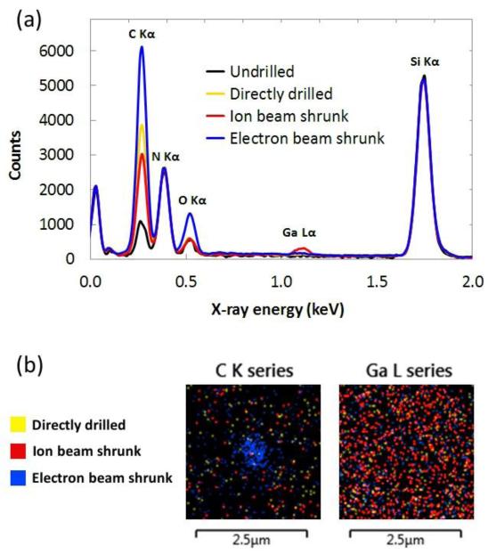
We also examined the elemental composition of nanopores and their surrounding areas. Figure 2 shows results from energy dispersive x-ray spectroscopy (EDS) measurements. We find striking differences between the three types of nanopore. First, from Figure 2a, we see that while each of the samples contains some carbon and oxygen, the amount present in the electron beam shrunk nanopore is significantly higher, consistent with increased electron beam deposition of ambient hydrocarbons from the microscope chamber.32 We note that this process is strongly dependent on vacuum chamber condition (i.e. when it was last cleaned, what type of pump is used, etc.) so variation in the amount and composition of deposited material from one microscope to another can be expected. Second, we observe that the only sample with an observable gallium peak is the ion beam shrunk nanopore, in keeping with incorporation of gallium into the silicon nitride as a result of prolonged exposure to the ion beam.
Figure 2.
Energy dispersive x-ray spectroscopy of nanopores. (a) Spectra taken from 500nm × 500nm square areas centered on each of three types of nanopore. The undrilled spectrum was taken on a remote section of the silicon nitride membrane. Spectra have been linearly scaled to match at the silicon peak. (b) Overlaid spatial distributions of carbon and gallium x-ray signals from the areas surrounding the same three nanopores.
Figure 2b shows the spatial distribution of carbon and gallium around the nanopores, and again the results are clearly correlated with the fabrication methods. During the electron beam shrinking process, the electron beam was rastered over a small area in the immediate vicinity of the nanopore, resulting in carbon deposition (and corresponding oxygen deposition, not shown) limited to that area. Since the electron beam used in these experiments did not damage the silicon nitride membrane even after prolonged exposure, we conclude that in the case of the electron beam shrunk nanopore, the final inner nanopore material consists entirely of deposited material, primarily hydrocarbons. No such localization of carbon is visible in the other nanopores.
During the ion beam shrinking process, the gallium ion beam was rastered over a much larger area to effectively lower the beam dose. Indeed, from Figure 2b, we see that gallium has been incorporated uniformly across the entire area (diameter ~800nm) surrounding the ion beam shrunk nanopore. Moreover, the amount of gallium is significantly higher than in the other nanopore samples, as would be expected from the single gallium peak in Figure 2a and from the much lower exposure to the ion beam that the other samples receive. We conclude that the ion beam shrunk nanopore contains some sizable fraction of gallium ions; unfortunately, reliable quantitative elemental percentage results could not be obtained from these samples because of the very thin material and therefore low number of x-ray counts.
Electrical Characterization
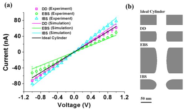
To study the electrical conductance of the nanopores, we obtained current-voltage (I-V) curves by sweeping the applied voltage and measuring the resultant ionic current (Figure 3a). The black line, which was calculated using COMSOL, shows what we would expect from a regular right cylinder that is 50nm wide and 50nm long. As expected from the geometrical characterization, the curves from the three nanopores described above deviate from that ideal. To identify the origin of this deviation, we numerically modeled the nanopores using COMSOL and obtained a quantitative estimation of I-V curves.
Figure 3.
(a) Experimental I-V curves (dots) of directly drilled (DD), electron beam shrunk (EBS) and ion beam shrunk (IBS) nanopores. The colored lines are the simulation results for three kinds of nanopores, while the black line represents an ideal 50nm cylinder. (b) The shapes of nanopores used for modeling. From top to bottom: ideal cylinder, directly drilled (DD) nanopore, electron beam shrunk (EBS) nanopore and ion beam shrunk (IBS) nanopore. Dimensions are to scale.
Our model improves on previous studies30,33,34 by taking into account the actual shape of the nanopores, as shown in Figure 3b. Our experimentally determined cross-sections were used to build 2D axisymmetric models to simultaneously solve the discretized Poisson, Nernst-Planck and Navier-Stokes equations with the finite element method and determine electric field, ion fluxes and velocity field. Our model uses cis and trans chambers that are 4μm in diameter and 2μm long, with a maximum mesh size on the nanopore surface of 1 nm. By including large chambers on either side of the nanopore, our model automatically incorporates access resistance, which we find to make a significant contribution to the overall resistance, although the nanopore itself still provides the bulk of the resistance. The constants used in our model are: T = 298K, Dk =1.957×10⁻⁹m2/s, Dcl = 2.032×10⁻⁹m2/s, ε = 80, η = 10−3Pa s, ρ =103kg/m3,zK =1,Zcl= −1,F =96485.3365C/mol, R = 8.31J/(mol ·K).
The solution to the coupled equations yields the ionic current through the nanopore by integrating the current density through a surface far away from the nanopore. In our simulation, we ignore the surface charge density of the nanopore because ion current rectification is experimentally found to be weak in 0.001M, 0.01M, 0.1M, 0.2M and 0.5M potassium chloride solutions35 and a linear dependence is found between the nanopore conductance and the KCl concentration36 (see supporting information). The good fit of our calculated I-V curves (colored lines in Figure 3a) suggests that the error caused by assuming electrically neutral surfaces is indeed negligible. In particular, we find that the directly drilled nanopore behaves very similar to the ideal cylinder while the EBS and IBS nanopores show significantly higher and lower resistance, respectively, consistent with their longer (EBS) or on-average wider (IBS) pore size.
Nanoparticle Detection
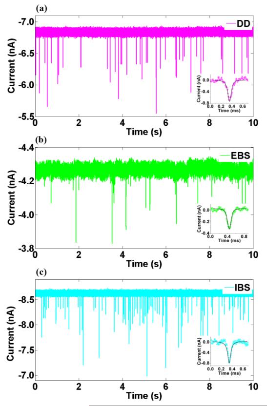
30 nm carboxyl polymer nanoparticles were used for particle translocation tests. As shown in Figure 4, when a 100mV voltage was applied, the baseline currents stabilized at different levels due to the different intrinsic resistance of each nanopore. As particles moved from the cis chamber into the trans chamber through the 50nm nanopore, they momentarily reduced the conductance of the nanopore, which we observe as blockades in the ionic current. The deviation of some blockade amplitudes may have been caused by the size distribution and aggregation of nanoparticles. Insets in Figure 4 show the comparison between typical blockade signals and the numerical simulations of the dynamic particle translocation process. The agreement is very good for all nanopore types.
Figure 4.
Signal traces of directly drilled (DD), electron beam shrunk (EBS) and ion beam shrunk (IBS) nanopores. Inserts are enlarged view of typical signals. Colored dots are experimental data and the black lines are blockades simulated using the numerical method. V = 100mV.
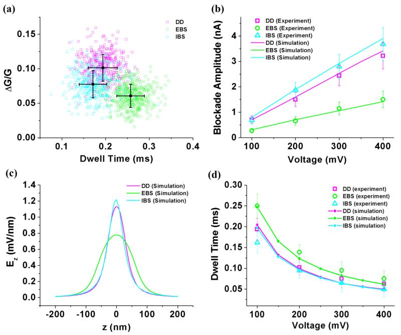
Figure 5a shows the relative change in conductance G of three nanopores as calculated for V=100mV using ΔG/G = ΔI/I, where ΔI is the amplitude of the blockade and I is the baseline current. The three nanopore types produced different conductance change distributions and dwell time distributions. The mean ΔG/G values from directly drilled, electron beam shrunk and ion beam shrunk nanopores are 0.10, 0.06 and 0.08, respectively. We note that the general trend in ΔG/G is consistent with the assumption that the relative conductance change is approximately equal to the ratio of particle volume to the nanopore volume,37 since the directly drilled nanopore (with the smallest volume) exhibits the biggest conductance change, while the electron beam shrunk nanopore (with the biggest volume) exhibits the smallest conductance change.
Figure 5.
(a) Scatter plot of events detected by three kinds of nanopores with V=100 mV. (b) The change of blockade amplitude versus the voltage. Dots are experimental results and lines are simulation results. (c) Simulated electric field strength along z axis of three kinds of nanopores. (d) Experimental and simulated dwell time versus voltage. Dots are experimental results and lines are simulation results.
Figure 5b shows the measured bias dependence of the current blockage amplitude, revealing a linear dependence for all three nanopore types. The blockade amplitude was also numerically calculated using the geometric model by introducing a particle and moving it from top to bottom along the z axis, with 5nm spacing between each calculation. At each point, the ionic current through the nanopore was calculated, with the results plotted as solid lines in Figure 5b. Once again, our geometric simulation agrees very well with the experimental results without any free fitting parameters. Since the bias dependence of the blockade amplitude is proportional to the conductance of the nanopore,38 it can be seen that the slope of the electron beam shrunk nanopore in Figure 5b is smaller than those of the other two nanopores due to its increased length.
Meanwhile, due to the deviation of the nanopores from a straight cylindrical shape, the electric field is expected to vary nonlinearly along each device. The simulation results shown in Fig. 5c confirm this expectation and again demonstrate that the electron-beam shrunk nanopore behaves significantly differently due to its shape.
To calculate the dwell time of a nanoparticle passing through the nanopore, we first calculate the local velocity of nanoparticle at each point along its trajectory using v=ε||ξpore|−|ξparticle||E/η,18,39 where ε, η, ξ and E are permittivity, viscosity, zeta potential and local electric field strength as determined above (Fig. 5c). The zeta potentials are unknown, so we simplify the expression to v = CE, where C is a constant. From the local velocity, we obtain an estimate of the time it takes for the nanoparticle to move between each point Δt = Δz/v, and the sum of the time intervals yields an estimate of the total dwell time tsum = Δt1 + Δt2 +…=(Δz1/E1 + Δz2/E2 +…)/C. We assume the zeta potentials of the nanopores are equal (and therefore the constants C are equal) and fit the simulation to the experimental data using a least squares fit (yielding C = 1.57×10⁻⁹ m2/Vs), as shown in Figure 5d. Simulated dwell times of the three nanopore types are inversely proportional to the applied voltage, and they match the experimental data well. While previous studies have focused on surface modification to predict and control dwell time, our work shows that the shape of nanopore plays a fundamental role in determining the speed of translocation.
Conclusion
In conclusion, we investigated the dependence of solid-state nanopore sensing of single nanoparticles on the physical and chemical properties of the nanopore. By cross-sectioning three types of nanopore, we found fabrication-dependent differences in their physical shape, ranging from hour-glass shaped cylinders to more conical funnels. In addition, we found that the chemical composition of the silicon membrane that carries the nanopore was altered, showing incorporation of hydrocarbons (electron-beam shrunk nanopore) and gallium (ion-beam shrunk nanopore). These differences in physical and chemical properties are summarized in Table 1.
Table 1.
Comparison of shape, mean diameter, length and composition between three kinds of nanopores with limiting apertures of 50nm. The mean diameter is the average taken along the length of each nanopore.
| Shape | Mean Diameter (nm) | Length (nm) | Composition | |
|---|---|---|---|---|
| DD | Cylinder | 52.2 | 50 | Silicon Nitride |
| EBS | Cylinder | 56.7 | 130 | Silicon Nitride, Hydrocarbon |
| IBS | Hour Glass | 64.1 | 50 | Silicon Nitride, Gallium |
Despite their nominally identical aperture, the electrical properties of the nanopores showed characteristic differences. Current-voltage characteristics, blockade amplitudes, and translocation dwell times were all dominated by the physical shape of the nanopores, not by their surface chemistry. This shows that the performance of solid-state nanopores as electrical biosensors can be understood and predicted once their three dimensional shape is known. Moreover, understanding how different fabrication methods, equipment, and conditions affect this geometry (and therefore sensing performance) can help identify the method of choice for a given application.
Methods
We fabricated solid-state nanopores with identical aperture diameter on commercially available 50nm thick silicon nitride membranes (DTF-050523, DuraSiN Film for TEM) with a dual beam microscope (FEI Quanta 3D FEG DualBeam SEM/FIB). We first milled the nanopores using the focused ion beam (30kV, 1.6pA) and then resized them to equal final diameters of 50nm. Directly drilled (DD) nanopores were milled to 50nm without resizing. Electron beam shrunk (EBS) nanopores were milled to a larger diameter and then resized to 50nm by rastering a low voltage, low current electron beam (5kV, 12pA) over the nanopore. Ion beam shrunk (IBS) nanopores were also milled to a larger diameter and then resized to 50nm by rastering across them with the same high voltage, low current ion beam used for the initial mill.23
Energy dispersive x-ray spectroscopy (EDS) measurements are performed using an Oxford Instruments AZtecEnergy microanalysis system with an X-MaxN 80 mm2 silicon drift detector.
All aqueous solutions were filtered with a 10nm filter (Whatman Antop 10) and the nanoparticles (Bangs Laboratories, Inc; PC02N/9934) were suspended in 0.2M potassium chloride solution (20mM CHES, pH=9, 0.01% v/v Triton X-100) at 5.16×10¹² particles/ml. Each nanopore membrane was clamped between two chambers (cis and trans) and flushed with isopropanol and deionized water. The nanoparticle solution was then added to the cis chamber and the electrolyte without nanoparticles to the trans chamber. An Axon Axopatch 200B patch clamp amplifier was used to apply the voltage across the nanopore. After filtering by an on board 100 kHz low-pass Bessel filter, the analog signal was digitized by an Axon Digidata 1440A digitizer at 250 kHz.
Supplementary Material
ACKNOWLEDGMENT
This work is supported by the NIH/NHGRI under grant 1R21HG006561-01 as well as the W.M. Keck Center for Nanoscale Optofluidics at the University of California at Santa Cruz. We gratefully acknowledge Aaron Drake and Sreenivas Bhattiprolu at Oxford Instruments and Mark Betts at Tescan for use of and assistance with the EDS microanalysis system.
Footnotes
Supporting Information Available: Change of nanopore diameter versus electron beam scanning time when 3 kV, 5 kV and 10 kV accelerating voltages are used, scanning electron micrographs of 50nm nanopores made on 100nm membranes and I-V curves of three types of nanopores in salt solutions of different concentrations. This material is available free of charge via the Internet at http://pubs.acs.org.
REFERENCES
- 1.Coulter WH. Means for Counting Particles Suspended in a Fluid. U.S. Patent 2,656,508. 1953 Oct 20; [Google Scholar]
- 2.Hogg WR, Coulter WH. Apparatus and Method for Measuring a Dividing Particle Size of a Particulate System. U.S. Patent 3,557,352. 1971 Jan 19; [Google Scholar]
- 3.DeBlois RW, Bean CP. Counting and Sizing of Submicron Particles by the Resistive Pulse Technique. Rev. Sci. Instrum. 1970;41:909–916. [Google Scholar]
- 4.Branton D, Deamer DW, Marziali A, Bayley H, Benner SA, Butler T, Ventra MD, Garaj S, Hibbs A, Huang X, et al. The Potential and Challenges of Nanopore Sequencing. Nat. Biotechnol. 2008;26 doi: 10.1038/nbt.1495. [DOI] [PMC free article] [PubMed] [Google Scholar]
- 5.Li J, Gershow M, Stein D, Brandin E, Golovchenko JA. DNA Molecules and Configurations in a Solid-State Nanopore Microscope. Nat. Mater. 2003;2:611–615. doi: 10.1038/nmat965. [DOI] [PubMed] [Google Scholar]
- 6.Meller A, Nivon L, Branton D. Voltage-Driven DNA Translocations Through a Nanopore. Phys. Rev. Lett. 2001;86:3435–3438. doi: 10.1103/PhysRevLett.86.3435. [DOI] [PubMed] [Google Scholar]
- 7.Akeson M, Branton D, Kasianowicz JJ, Brandin E, Deamer DW. Microsecond Time-Scale Discrimination Among Polycytidylic Acid, Polyadenylic Acid, and Polyuridylic Acid as Homopolymers or as Segments Within Single RNA Molecules. Biophys. J. 1999;77:3227–3233. doi: 10.1016/S0006-3495(99)77153-5. [DOI] [PMC free article] [PubMed] [Google Scholar]
- 8.Storm AJ, Storm C, Chen JH, Zandbergen H, Joanny JF, Dekker C. Fast DNA Translocation through a Solid-State Nanopore. Nano Lett. 2005;5:1193–1197. doi: 10.1021/nl048030d. [DOI] [PubMed] [Google Scholar]
- 9.Kasianowicz JJ, Brandin E, Branton D, Deamer DW. Characterization of Individual Polynucleotide Molecules Using a Membrane Channel. PNAS. 1996;93:13770–13773. doi: 10.1073/pnas.93.24.13770. [DOI] [PMC free article] [PubMed] [Google Scholar]
- 10.Derrington IM, Butler TZ, Collins MD, Manrao E, Pavlenok M, Niederweis M, Gundlach JH. Nanopore DNA Sequencing with MspA. PNAS. 2010;107:16060–16065. doi: 10.1073/pnas.1001831107. [DOI] [PMC free article] [PubMed] [Google Scholar]
- 11.Dekker C. Solid-State Nanopores. Nat. Nanotechnol. 2007;2:209–215. doi: 10.1038/nnano.2007.27. [DOI] [PubMed] [Google Scholar]
- 12.Garaj S, Hubbard W, Reina A, Kong J, Branton D, Golovchenko JA. Graphene as a Subnanometre Trans-Electrode Membrane. Nature. 2010;467:190–193. doi: 10.1038/nature09379. [DOI] [PMC free article] [PubMed] [Google Scholar]
- 13.Healy K, Schiedt B, Morrison AP. Solid-state Nanopore Technologies for Nanopore-Based DNA Analysis. Nanomedicine (London, U. K.) 2007;2:875–897. doi: 10.2217/17435889.2.6.875. [DOI] [PubMed] [Google Scholar]
- 14.Park SR, Peng H, Ling XS. Fabrication of Nanopores in Silicon Chips Using Feedback Chemical Etching. Small. 2007;3:116–119. doi: 10.1002/smll.200600268. [DOI] [PubMed] [Google Scholar]
- 15.Wanunu M, Dadosh T, Ray V, Jin J, McReynolds L, Drndić M. Rapid Electronic Detection of Probe-Specific microRNAs Using Thin Nanopore Sensors. Nat. Nanotechnol. 2010;5:807–814. doi: 10.1038/nnano.2010.202. [DOI] [PubMed] [Google Scholar]
- 16.Garaj S, Hubbard W, Reina A, Kong J, Branton D, Golovchenko JA. Graphene as a Subnanometre Trans-Electrode Membrane. Nature. 2010;467:190–193. doi: 10.1038/nature09379. [DOI] [PMC free article] [PubMed] [Google Scholar]
- 17.Kuan AT, Golovchenko JA. Nanometer-Thin Solid-State Nanopores by Cold Ion Beam Sculpting. Appl. Phys. Lett. 2012;100:213104–213104-4. doi: 10.1063/1.4719679. [DOI] [PMC free article] [PubMed] [Google Scholar]
- 18.Davenport M, Healy K, Pevarnik M, Teslich N, Cabrini S, Morrison AP, Siwy ZS, Létant SE. The Role of Pore Geometry in Single Nanoparticle Detection. ACS Nano. 2012;6:8366–8380. doi: 10.1021/nn303126n. [DOI] [PubMed] [Google Scholar]
- 19.Lanyon YH, Marzi De G, Watson YE, Quinn AJ, Gleeson JP, Redmond G, Arrigan DWM. Fabrication of Nanopore Array Electrodes by Focused Ion Beam Milling. Anal. Chem. 2007;79:3048–3055. doi: 10.1021/ac061878x. [DOI] [PubMed] [Google Scholar]
- 20.Patterson N, Adams DP, Hodges VC, Vasile MJ, Michael JR, Kotula PG. Controlled Fabrication of Nanopores Using a Direct Focused Ion Beam Approach with Back Face Particle Detection. Nanotechnology. 2008;19:235304. doi: 10.1088/0957-4484/19/23/235304. [DOI] [PubMed] [Google Scholar]
- 21.Schiedt B, Auvray L, Bacri L, Oukhaled G, Madouri A, Bourhis E, Patriarche G, Pelta J, Jede R, Gierak J. Direct FIB Fabrication and Integration of “Single Nanopore Devices” for the Manipulation of Macromolecules. Microelectron. Eng. 2010;87:1300–1303. [Google Scholar]
- 22.Cai Q, Ledden B, Krueger E, Golovchenko JA, Li J. Nanopore Sculpting with Noble Gas Ions. J. Appl. Phys. 2006;100:24914–249146. doi: 10.1063/1.2216880. [DOI] [PMC free article] [PubMed] [Google Scholar]
- 23.Holmes MR, Shang T, Hawkins AR, Rudenko M, Measor P, Schmidt H. Micropore and Nanopore Fabrication in Hollow Antiresonant Reflecting Optical Waveguides. J. Micro/Nanolithogr., MEMS, MOEMS. 2010;9:023004. doi: 10.1117/1.3378152. [DOI] [PMC free article] [PubMed] [Google Scholar]
- 24.Storm AJ, Chen JH, Ling XS, Zandbergen HW, Dekker C. Fabrication of Solid-State Nanopores with Single-Nanometre Precision. Nat. Mat. 2003;2:537–540. doi: 10.1038/nmat941. [DOI] [PubMed] [Google Scholar]
- 25.Kox R, Chen C, Lagae L, Borghs G. Shrinking Solid-State Nanopores and Nanoslits Using Electron Beam Induced Deposition with Different Precursors. In IEEE Conf. Nanotechnol. (9th) 2009:605–608. doi: 10.1088/0957-4484/20/11/115302. [DOI] [PubMed] [Google Scholar]
- 26.Li J, Stein D, McMullan C, Branton D, Aziz MJ, Golovchenko JA. Ion-Beam Sculpting at Nanometre Length Scales. Nature. 2001;412:166–169. doi: 10.1038/35084037. [DOI] [PubMed] [Google Scholar]
- 27.Erlebacher J, Aziz MJ, Chason E, Sinclair MB, Floro JA. Spontaneous Pattern Formation on Ion Bombarded Si(001) Phys. Rev. Lett. 1999;82:2330–2333. [Google Scholar]
- 28.Cai Q, Ledden B, Krueger E, Golovchenko JA, Li J. Nanopore Sculpting with Noble Gas Ions. J. Appl. Phys. 2006;100:024914–024914-6. doi: 10.1063/1.2216880. [DOI] [PMC free article] [PubMed] [Google Scholar]
- 29.Kwong WY, Zhang WY. Electron-Beam Assisted Platinum Deposition as a Protective Layer for FIB and TEM Applications; In ISSM 2005, IEEE Int. Symp. Semicond. Manuf., Conf. Proc.; 2005.pp. 469–471. [Google Scholar]
- 30.He Y, Tsutsui M, Fan C, Taniguchi M, Kawai T. Controlling DNA Translocation through Gate Modulation of Nanopore Wall Surface Charges. ACS Nano. 2011;5:5509–5518. doi: 10.1021/nn201883b. [DOI] [PubMed] [Google Scholar]
- 31.Yalcin SE, Lee SY, Joo SW, Baysal O, Qian S. Electrodiffusiophoretic Motion of a Charged Spherical Particle in a Nanopore. J. Phys. Chem. B. 2010;114:4082–4093. doi: 10.1021/jp100784p. [DOI] [PubMed] [Google Scholar]
- 32.Ennos AE. The Origin of Specimen Contamination in the Electron Microscope. Br. J. Appl. Phys. 1953;4:101–106. [Google Scholar]
- 33.White HS, Bund A. Ion Current Rectification at Nanopores in Glass Membranes. Langmuir. 2008;24:2212–2218. doi: 10.1021/la702955k. [DOI] [PubMed] [Google Scholar]
- 34.Ai Y, Zhang M, Joo SW, Cheney MA, Qian S. Effects of Electroosmotic Flow on Ionic Current Rectification in Conical Nanopores. J. Phys. Chem. C. 2010;114:3883–3890. [Google Scholar]
- 35.Lan W-J, Holden DA, Zhang B, White HS. Nanoparticle Transport in Conical-Shaped Nanopores. Anal. Chem. 2011;83:3840–3847. doi: 10.1021/ac200312n. [DOI] [PubMed] [Google Scholar]
- 36.Stein D, Kruithof M, Dekker C. Surface-Charge-Governed Ion Transport in Nanofluidic Channels. Phys. Rev. Lett. 2004;93:035901. doi: 10.1103/PhysRevLett.93.035901. [DOI] [PubMed] [Google Scholar]
- 37.Saleh OA, Sohn LL. An Artificial Nanopore for Molecular Sensing. Nano Lett. 2003;3:37–38. [Google Scholar]
- 38.Petrossian L, Wilk SJ, Joshi P, Goodnick SM, Thornton TJ. Demonstration of Coulter Counting through a Cylindrical Solid State Nanopore. J. Phys.: Conf. Ser. 2008;109:012028. [Google Scholar]
- 39.Firnkes M, Pedone D, Knezevic J, Döblinger M, Rant U. Electrically Facilitated Translocations of Proteins through Silicon Nitride Nanopores: Conjoint and Competitive Action of Diffusion, Electrophoresis, and Electroosmosis. Nano Lett. 2010;10:2162–2167. doi: 10.1021/nl100861c. [DOI] [PubMed] [Google Scholar]
Associated Data
This section collects any data citations, data availability statements, or supplementary materials included in this article.


