Abstract
Flexible electronics are a very promising technology for various applications. Several types of flexible devices have been developed, but there has been limited research on flexible electromechanical systems (MEMS). Surface acoustic wave (SAW) devices are not only an essential electronic device, but also are the building blocks for sensors and MEMS. Here we report a method of making flexible SAW devices using ZnO nanocrystals deposited on a cheap and bendable plastic film. The flexible SAW devices exhibit two wave modes - the Rayleigh and Lamb waves with resonant frequencies of 198.1 MHz and 447.0 MHz respectively, and signal amplitudes of 18 dB. The flexible devices have a high temperature coefficient of frequency, and are thus useful as sensitive temperature sensors. Moreover, strong acoustic streaming with a velocity of 3.4 cm/s and particle concentration using the SAW have been achieved, demonstrating the great potential for applications in electronics and MEMS.
Flexible electronic devices such as field effect transistors and their associated integrated circuits1,2 are central to many applications such as displays3,4, eyeball cameras5, memory6 and lithium-ion batteries7. Flexible microelectromechanical systems (MEMS) add to the flexible electronic devices family, and have important and widespread applications. Various MEMS devices and systems have been developed such as the micro-machined infrared bolometer8, piezoelectric actuators9, thin film bulk acoustic wave resonators10, piezoelectric pressure sensors11, and microfluidics12. Surface acoustic wave (SAW) devices are crucial for the development of many MEMS devices and systems as they are the fundamental building blocks for microsensors and microsystems13,14,15,16,17,18,19,20,21,22,23,24. However, the lack of an effective approach for the manufacture of flexible and high performance SAW devices has been the major obstacle to the exploitation of many proposed flexible electronic applications for sensors and MEMS, especially in microfluidics and lab-on-a-chip.
SAW devices have a very wide range of applications including their use in radio-frequency communication as filters, frequency duplexers and RF tags (RFIDs), in biochemical sensing, drug development, healthcare, medical and life sciences as micro-sensors for measuring physical parameters and detecting biochemical substances13,14,15,16,17,18,19, and micro-actuators for microfluidics21,22 as well as for lab-on-a-chip applications22,23,24. SAW devices are normally made on piezoelectric (PE) substrates such as LiNbO3, or on PE thin films such as zinc oxide (ZnO) or aluminum nitride (AlN) deposited on rigid substrates such as silicon (Si) or sapphire. It would be a huge benefit if SAW devices can be constructed at low cost on a cheap and flexible substrate such as on plastic films, which may be either disposable or recyclable. But so far there is no report of such SAW devices because of the difficulties in achieving the growth of high-quality PE films with large areas on a flexible substrate25. It is especially difficult to obtain highly c-axis oriented, low surface roughness PE films with a good piezoelectric constant. The following factors may be particularly responsible for the current situation: (1) Most flexible substrates are amorphous, hence they do not match the lattices of the required PE crystals; (2) The large differences in the thermal expansion coefficients between the substrates and the PE films cause serious problems in the film deposition26; (3) SAW devices generally demand thick PE layers (the thickness must be larger than 10% of the SAW wavelength), which makes film growth and fabrication processing difficult. In this paper, we report a method of making flexible SAW devices using ZnO nanocrystals deposited on a polyimide (PI) substrate − a cheap, bendable and disposable plastic film. We describe their excellent transmission properties, strong acoustic streaming and particle sorting capabilities to demonstrate their potential applications in flexible electronic devices, sensing, microfluidics and lab-on-a-chip.
Results
Nanocrystalline ZnO piezoelectric films
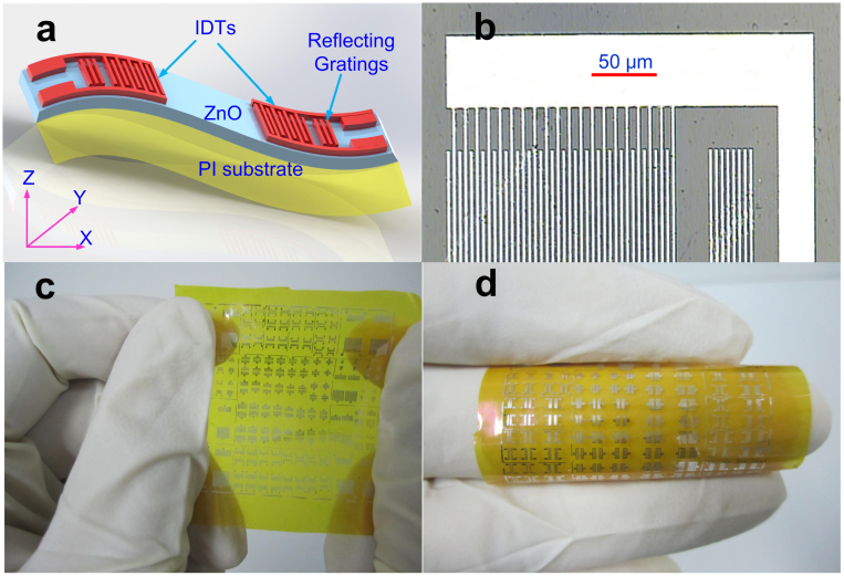
To make the flexible SAW devices, a Kapton® polyimide film 100 H (Toray, Dupont, thickness 100 μm) was chosen as the substrate because of its excellent flexibility, good mechanical and electrical properties, its chemical stability, and its wide operating temperature range (−269 to 400°C)27. Figure 1 shows a schematic drawing of the structure of the device (Figure 1a), a microscopic top view of the interdigitated transducer (IDT) electrode (Figure 1b), and photographs of the fabricated devices on the PI film (Figure 1c and 1d). In this work, three different groups of devices, denoted as A, B and C, have been fabricated using conventional ultraviolet photolithography techniques and a simple lift-off process. In group A, the thickness of the ZnO films was fixed at 4 μm, while the acoustic wavelength, λ, was varied to be λ = 10 μm, 12 μm, 16 μm, 20 μm, 24 μm, and 32 μm, respectively, by changing the IDT finger spacing. In group B and C devices, the wavelengths were fixed at 16 μm and 12 μm respectively, while the thickness of the ZnO films was varied from 1.7 μm to 4 μm. The detailed parameters of these three groups of devices are summarized in Tables S1 and S2 in the Supplementary Information (SI).
Figure 1. The flexible thin film ZnO/polyimide SAW devices.
(a) Three-dimensional schematic of the developed SAW device on a ZnO/polymer substrate; (b) Microscope image of a SAW device with 20 pairs of interdigitated transducers (IDT) figure; (c) & (d) Photographs of semi-transparent and flexible SAW devices on polyimide.
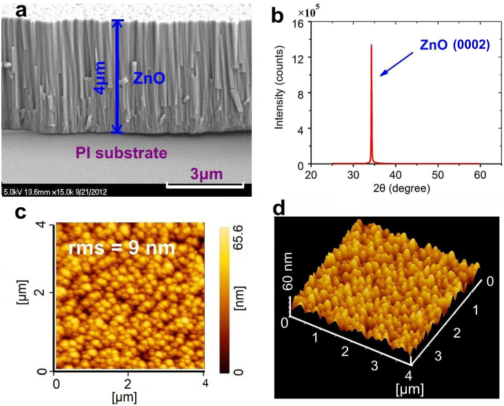
The ZnO films were made up of vertically-aligned ZnO nanocrystals deposited on the PI substrates using a home-made direct-current magnetron sputtering system. A water-cooled zinc target of purity 99.999% was employed for the deposition under a flow of O2/Ar mixture with a deposition pressure of 2 Pa (see SI for details). Figure 2a shows a scanning electron microscope (SEM) photo of a 4 μm thick ZnO thin film as an example. It can be seen that the ZnO film consists of highly-oriented columnar nanograins perpendicular to the substrate, a growth result similar to what has been previously achieved on Si substrates28,29. X-ray diffraction (XRD) characterization reveals that the (0002) ZnO crystal orientation dominates the crystal orientation (Figure 2b). The full-width at half-maximum (FWHM) of the XRD peak is 0.152° and is comparable with most of the results obtained from thin films of ZnO deposited on rigid substrates, demonstrating the high crystalline quality of the thin films deposited on the polymer substrates.
Figure 2. Characterization of ZnO thin film deposited on polyimide substrate.
(a) An SEM image of the cross-section; (b) XRD pattern of the ZnO layer; (c) & (d) AFM images. The root mean square of the surface roughness is about 9 nm.
The mean crystallite grain size, D, was estimated to be ~ 72.3 nm using the Debye–Scherrer formula30 (see SI for details), similar to the ZnO nanorods previously deposited on solid substrates31. The biaxial stress which is less than 100 MPa for all the films deposited was estimated from the lattice constant obtained from the XRD patterns. This enables the films to be directly used for the fabrication of SAW devices without any thermal annealing to remove the stress in the films. Figure 2c and 2d show the morphology and surface roughness of the films measured by atomic force microscopy (AFM). Here the root mean square (RMS) roughness was estimated to be ~ 9 nm over an area of 4 × 4 μm2, comparable to those obtained from the films deposited on solid substrates32,33, suggesting that the films are sufficiently smooth for the fabrication of SAW devices. A smooth surface of PE films is necessary for the fabrication of SAW devices with high performance and it also allows the fabrication of smooth IDT electrodes. This will reduce wave scattering by the PE layer and the IDT electrodes, hence reducing the transmission loss.
SAW transmission characteristics
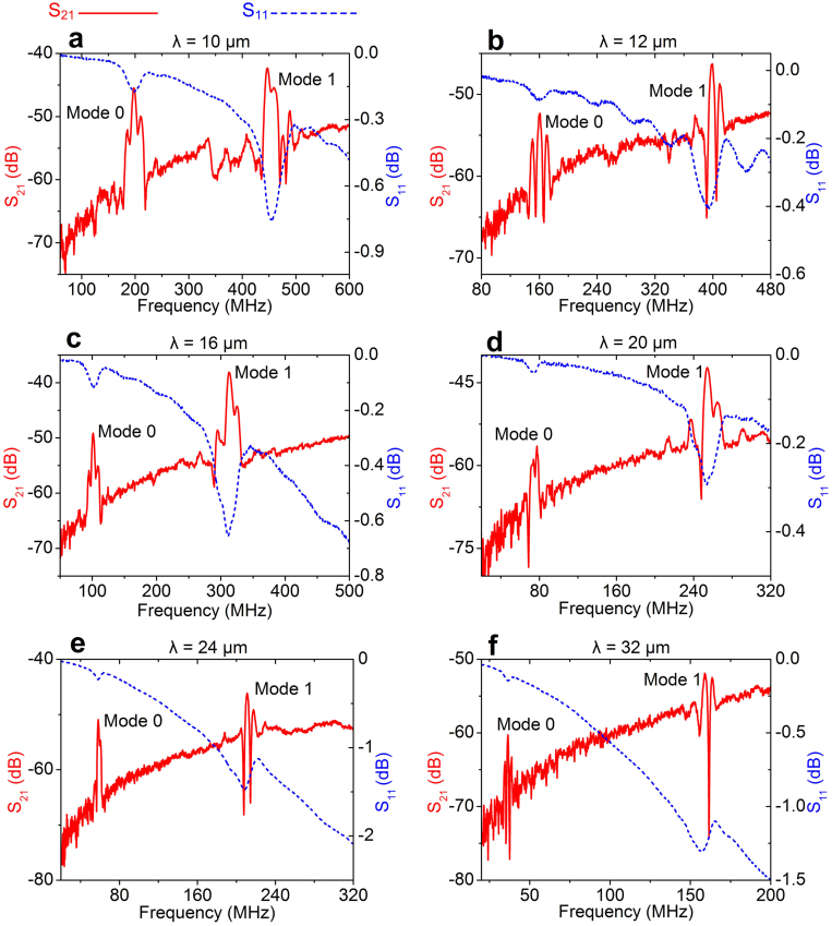
The transmissions (S21) and reflections (S11) of all the group A devices (4 μm thick ZnO with varying wavelength from 10 to 32 μm) exhibit two well-defined resonant peaks (Figure 3). The zero mode resonant peak with a frequency, f0, of 34.4, 56.4, 75.0, 101.5, 161.0 and 198.1 MHz respectively, and the first mode resonant peak with a frequency, f1, varying in the range from 158.5 to 447.0 MHz, both correspond to the respective wavelength of 32, 24, 20, 16, 12 or 10 μm (See Table S1 in SI). A large transmission signal amplitude of up to ~ 18 dB was obtained for both the wave modes, indicating that the performance of the fabricated flexible SAW devices is sufficient for electronic and communication applications. It was also observed that in most fabricated devices, the signal amplitude of the first resonant mode is higher than that of the zero resonant one, suggesting that the first mode resonance can be better used for high frequency applications. Moreover, our finite element analysis (FEA) (see SI for details) has revealed the nature of the two resonant modes: the zero mode resonance corresponds to the Rayleigh wave, and the first mode to the Lamb wave. Rayleigh waves are a type of acoustic wave travelling near the surface of the PE substrate with particle motion perpendicular to the surface and the amplitude decreases exponentially with increase in penetration depth. Lamb waves are a type of wave similar to Rayleigh waves but are bound within a plate.
Figure 3. Transmission spectrum of the flexible ZnO/polyimide SAW devices with 4 (m thick ZnO film as a function of wavelength,  , (a) (
 = 10 μm; (b) 12 μm; (c) 16 μm; (d) 20 μm; (e) 24 μm and (f) 32 μm.
Two well-defined resonant modes with high amplitude were obtained from all devices with different wavelengths. All the SAW devices have 20 pairs of IDT fingers.
When the wavelength is short, the transmission spectra showed two well-defined resonant peaks but the shape becomes distorted with dips near the central frequency even larger than the amplitude of the resonant peaks as shown in Figure 3e and 3f. This is especially so for that of the Lamb waves. Incoherent resonance by individual IDT fingers is responsible for the dips, and it becomes more pronounced at longer wavelengths where more of the acoustic waves penetrate into the polymer substrate.
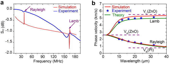
To understand more about the experimental results, we have performed simulations and theoretical analyses34 on the resonant frequencies and phase velocities (see SI for details). Figure 4a shows an example for comparison between the experimental reflection spectrum (S11) and the simulated one from the FEA simulation. It can be seen that the two resonant peaks are roughly consistent with one another in position although the amplitudes of the experimental ones are much smaller due to the polycrystalline nature of the actual films whereas an ideal single crystal structure is assumed for the simulation and theoretical calculations. Similarly, Figure 4b illustrates the results of the experimental phase velocities (vpi) and the simulated and calculated ones for both the Rayleigh and the Lamb wave modes. Here the velocity is determined from vpi = λifi (i = 0 or 1, corresponding to the Rayleigh or the Lamb wave) at fixed wavelengths of λi = 32, 24, 20, 16, 12 and 10 μm, respectively. Clearly, vp0 increases from 1101 to 1981 m/s, and vp1 decreases from 5072 m/s to 4470 m/s with decrease in wavelength. The theoretical calculations of the phase velocities agree well with the experimental and the simulated ones, implying that the models used for the analyses and modeling are accurate.
Figure 4. The experimental and simulation spectra (a) and phase velocity (b) of the flexible ZnO/polyimide SAW devices with a 4 μm thick ZnO thin film as a function of wavelength.
The wavelength used for simulating the spectrum in (a) is 32 μm. The two well defined resonant peaks are in good agreement with the experimental result. As the wavelength increases, the phase velocity of the Rayleigh wave decreases and approaches the Rayleigh wave velocity in the polymer substrate, while the phase velocity of the Lamb wave increases and approaches that in the ZnO layer. The SAW devices have 20 pairs of IDT fingers.
For a layered structure, the phase velocity is influenced by the intrinsic properties of the piezoelectric layer and the substrate. In an ideal (0002) ZnO layer, the theoretical phase velocity limit of the Rayleigh mode would be ~ 2650 m/s, while this velocity in polyimide is much smaller and is estimated to be ~ 754 m/s (see SI for details). In this case, when the wavelength is reduced, the acoustic waves will be more confined in the ZnO layer. At a short wavelength of λ = 10 μm, which is 2.5 times the ZnO film thickness, the phase velocity (~1981 m/s in this case) already reaches ~ 75% of the theoretical limit of the ZnO, demonstrating the excellent properties of the deposited films and the SAW devices fabricated. Since the phase velocity in ZnO is much higher than that in polyimide, the Lamb waves are expected to co-exist in this layered structure35, as has been confirmed by our experiments and simulation.
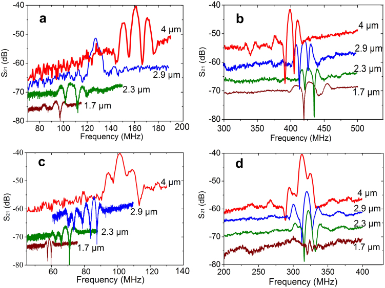
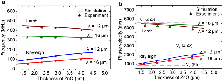
In addition to the materials used to make the layered structure, it should be noted that the ZnO film thickness has a strong effect on both the resonant frequency and the phase velocity of the Rayleigh and Lamb waves. This thickness effect was tested by fixing the wavelength at either λ = 16 μm or 12 μm (Figure 5, and Table S2 in SI). It was found that both the resonant frequency (f0) and phase velocity (vp0) of the Rayleigh wave increased with increase in film thickness. However, for the Lamb wave, the film thickness showed the opposite effect, i.e., the increase in film thickness reduces the values of f1 and vp1. For comparison, the simulated results are also shown in Figure 6. It can be seen that at both scanned wavelengths, vp1 approaches its limit of ~ 5510 m/s in an extremely thin ZnO layer, and that the change of frequencies from device to device is indeed caused by the variation of the ZnO thickness and wavelength.
Figure 5. The effect of the thickness of ZnO film on the resonant responses of the Rayleigh wave and the Lamb wave of the flexible Al/ZnO/polyimide SAW devices with a wavelength of 12 μm for (a) the Rayleigh wave, and (b) the Lamb wave; A wavelength of 16 μm was used for (c) the Rayleigh wave, and (d) the Lamb wave.
The SAW devices have 20 pairs of IDT fingers. (the different spectra are presented on top of each other for clarity).
Figure 6. Comparison of experiments and FEA simulation results on the resonant frequency (a) and phase velocity (b) vs. thickness of ZnO film at different wavelengths.
The lines are obtained from simulation, whereas the symbols are the experimental data. The SAW devices have 20 pairs of IDT fingers.
Based on the above results, we conclude that a Rayleigh wave resonant frequency f0 of 198.1 MHz, vp of 1981 m/s and an electromechanical coupling coefficient (K2) of 1.05%, and a Lamb wave resonant frequency f1 of 447 MHz, vp1 of 4470 m/s and K2 of 0.8% have been obtained in this work (See SI for details). The slightly larger values of the simulated results compared to the experimental data as shown in Figure 6b are probably due to the use of the ideal material constants for the simulation, which are certainly better than the actual ones for the ZnO film and the polyimide as these layers may have defects and a damaged surface caused by ion bombardment during the deposition. However, the overall excellent performance, especially the high resonant frequencies and large transmission signals of both the Rayleigh and Lamb waves, demonstrate that our flexible SAW devices have great potential for electronics, sensors and lab-on-a-chip applications.
Flexible SAW temperature sensor
It is well known that SAW devices are extremely useful for the development of various types of sensors owing to their high sensitivity17 and wireless capability. For instance, mass-loading based SAW sensors have a much higher sensitivity for biodetection compared to electrochemical sensors etc. as they have very high resonant frequency and a thin active layer (about one wavelength deep). This leads to a small base mass. SAW devices have been utilized as wireless sensors for monitoring changes of various physical parameters such as temperature13 and pressure14,36 because of their structural simplicity and easy operation. Flexible SAW devices can play an important role in this respect owing e.g. to the thin film structure and low cost. Furthermore SAW devices can be used for microfluidics and lab-on-a-chip applications37 owing to their large actuation force, high flow velocity and non-moving component characteristics. In fact, they have been used for biodetection and liquid pumping and mixing. If flexible SAW devices can be proven to be useful for high performance sensors and microfluidics, this will open the door for widespread applications for inexpensive and disposable lab-on-a-chip applications for healthcare, medical research and biotechnologies. As examples, we have conducted experiments on temperature sensing, acoustic wave-induced streaming and particle concentration and sorting using the flexible SAW devices developed in this work to verify their suitability for these applications.
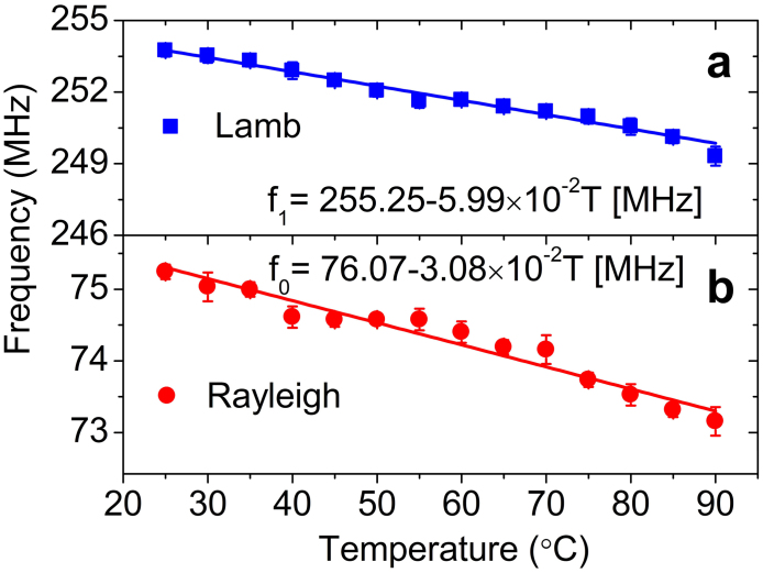
The resonant frequencies of the Rayleigh and Lamb waves of the flexible SAW devices have been obtained as a function of temperature with the results shown in Figure 7. The frequencies measured for both the wave modes decrease linearly with increase in temperature, which is the same trend as observed from other SAW devices built on rigid substrates37,38. The temperature coefficients of frequency (TCF), defined as Δf/ΔTf0, are ~ 442 and ~ 245 ppm/K for the zero and first modes respectively, and are almost constant for devices with different wavelengths and from different substrates. Both of these values are much larger than the TCF of the Rayleigh wave from the rigid ZnO/Si (~67 ppm/K)38 and the bulk LiNbO3 (70–80 ppm/K)37 SAW devices. This is attributed to the much larger thermal expansion coefficient of the polyimide substrate (20 ppm/K, Dupont database) than that of the Si substrate (~3.0 ppm/K). Therefore, the excellent linearity and large TCFs of the flexible SAW devices make them better than those reported for rigid SAW devices for the development of sensitive temperature sensors for measurements, calibrations or as a reference for other sensing systems.
Figure 7. Resonant frequency as a function of temperature for the zero mode wave (a) and the first mode wave (b).
The resonant frequencies decrease linearly with increase of the temperature showing a TCF of 442 and 245 ppm/K for the zero and first mode wave respectively. The SAW devices have a wavelength of 20 μm and 20 pairs of IDT fingers.
Flexible SAW microfluidics
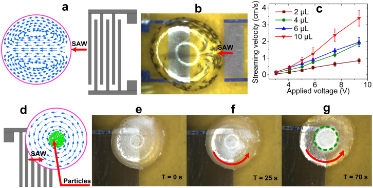
When a liquid droplet is located in the path of a surface acoustic wave, the SAW will interact with the liquid and the acoustic energy will be coupled into the liquid, inducing acoustic streaming as schematically shown in Figure 8a. This has been utilized for pumping22, mixing19, atomization39, particle concentration and sorting40,41. We found that the flexible SAW devices can provide the same functions as those built on solid and unbendable substrates. Figure 8b is a snap shot of the acoustic streaming inside a 2 μL droplet induced by the Rayleigh wave from a flexible SAW device, showing stable streaming with a double vortex pattern similar to those obtained from SAW devices on stiff substrates21. The acoustic streaming can be viewed from the Movie in the Supplementary Information section. The SAW devices used for this experiment have a resonant frequency of f0 = 161.1 MHz (Device A2). Figure 8c shows the streaming velocities measured at the centre of droplets of different sizes as a function of RF signal voltage. The streaming velocities were found to increase almost linearly with increase of RF signal voltage applied to the IDT electrodes. These velocities also increase with increase in droplet size, and reach 3.4 cm/s at a signal voltage of 9.5 V for a 10 μL droplet. Although the streaming velocities are lower than those of SAW devices on rigid substrates40, it is more than enough for flexible SAW devices to be used for most microfluidic applications.
Figure 8.
(a) A schematic drawing of acoustic streaming inside a liquid droplet, (b) a snapshot of acoustic streaming induced by the flexible SAW device, showing a double vortex streaming pattern. (c) Streaming velocity as a function of RF signal voltage with droplet size as a parameter, showing a linear increase in streaming velocity with signal voltage. (d) A schematic drawing to show circulating streaming and particle concentration induced by SAW off the central wave path. Particles are uniformly distributed in liquid (e) and partial concentration in the droplet after applying a RF signal for 25 sec (f) and 70 sec (g) with a signal voltage of 25 V. The SAW device used for these experiments has 50 pairs of IDT fingers, and a wavelength of 12 μm. Only the Rayleigh Wave was used for microfluidic experiments. The red curved arrows are indicative of the streaming direction, and the green circle shows the area with the highly concentrated nanoparticles.
The flexible SAW devices have also been tested for the ability to perform particle concentration and sorting functions, one of many lab-on-a-chip applications in biotechnology and medical science. Here the droplet containing TiO2 nano-particles is positioned off the central line of the wave path, which allows the SAW to induce a circulating streaming pattern, generating a shear force which pushes particles towards the center of the droplet40 as shown in Figure 8d. Figure 8e, 8f and 8g show the sequence of the particle concentration under a SAW. Uniformly distributed nano-particles are moved towards the centre of the droplet after a RF signal with a peak-to-peak voltage of 25 V is applied to the IDT electrode. The nano-particles were concentrated in the centre of the droplet after ~ 70 seconds. The results show that the flexible SAW devices can indeed be used for microfluidics and lab-on-chip applications with similar excellent performance to those made on bulk PE substrates40 or on PE films deposited on rigid substrates21,39,41.
Discussion
The two resonant frequencies of the reflection spectrum obtained experimentally are roughly consistent with the simulated ones as shown in Figure 4a, but the amplitudes of the experimental ones are much smaller than the modeling results. This is mainly due to the use of polycrystalline ZnO material for the device whereas an ideal single crystal structure is assumed for the simulation. Also the simulated spectra showed some differences from the experimental ones with one upward peak as well as one downward peak. For an ideal SAW device, the reflection spectrum normally should have two closely-positioned resonant frequencies, namely the series resonant frequency, fs, (corresponding to the downward peak) and the parallel resonant frequency, fp, (the upward peak)42. The large parallel resonant peak obtained from the simulation is due to the use of the ideal device and crystal structure with no defects and no surface roughness, and the use of one pair of the IDT fingers with expansion by repetition to an infinite plane with no boundary edges. Practical SAW devices typically have a very small parallel resonant peak due to the existence of defects and imperfect device structures, and small device area.
The fabricated SAW devices on PI substrates have demonstrated their potential for applications in electronics, sensors and lab-on-a-chip. However both the signal amplitudes and the base lines of the SAW devices are rather small and low. These are believed to be affected by electromechanical coupling or transmission loss during propagation. According to the equivalent circuit of a SAW transducer, the electromechanical coupling coefficient can be evaluated from43
where N is the number of finger pairs and Gm (f0) and Bs (f0) are respectively the motional conductance and static susceptance of the input port at f0. A K2 value of 1.05% was obtained for the Rayleigh wave with f0 = 198.1 MHz, and 0.8% for the Lamb wave with f1 = 447 MHz for Device A1, and was even smaller for those with longer wavelengths or thinner ZnO layers. These values are smaller than those obtained from SAW on ZnO on solid substrates, implying a high attenuation coefficient from the polymer substrates. The small K2 values are responsible for the slow acoustic streaming velocities and longer time for the particle concentration observed. However it should be pointed out that for most lab-on-chip applications, a flow velocity of up to one millimeter/s is sufficient. Therefore the results have clearly demonstrated that the flexible SAW performances are sufficient for applications in microfluidics and lab-on-a-chip. Furthermore, the signal amplitude up to 18 dB for both the zero and first mode waves is also sufficient for communication applications.
In summary, ZnO piezoelectric thin films have been deposited on flexible polyimide substrates at low temperature by reactive magnetron sputtering. The ZnO thin films have (0002) orientation, columnar grain structure and small surface roughness. Flexible ZnO/polyimide SAW devices have been fabricated. All the flexible SAW devices showed two resonant modes: the Rayleigh wave and Lamb wave with a resonant frequency and coupling coefficient of 198.1 MHz and 1.05%, and of 447 MHz and 0.8% respectively. Both the wave modes have a much larger TCF than those built on rigid substrates, hence are better for high sensitivity temperature sensors. Furthermore, strong acoustic streaming with a velocity of up to 3.4 cm/s and particle concentration using SAW have been achieved. The results are comparable to those obtained from SAW devices made on rigid substrates. All these results have clearly demonstrated that our flexible SAW devices have great potential for applications in electronics and microsystems.
Methods
ZnO deposition on polymer substrates
ZnO thin films were deposited on the polymer substrates (Kapton® polyimide film 100 H) using a direct-current (DC) magnetron sputtering system built in our laboratory. The base pressure of the chamber was 1 × 10⁻⁴ Pa before deposition. A water-cooled zinc target of purity 99.999% with a diameter of 100 mm was used for the deposition of the ZnO films. The distance between the target and the substrate was fixed at 70 mm. The deposition conditions are as follows: O2/Ar mixture gas has a ratio of 50/100 (sccm); the deposition pressure is 2 Pa; the DC sputtering power is 200 W; the substrate temperature is fixed at 100°C, and the bias voltage is −75 V.
Crystal structure characterization
The crystalline structure of the ZnO films was analyzed using X-ray diffraction (XRD) (Panalytical Empyrean) with Cu- radiation (λ = 0.154 nm) at 40 keV and 40 mA. The diffraction patterns were obtained in the 2θ mode with a scan range of 2θ = 20° ~ 70°. For cross-sectional structural analysis, a scanning electron microscope (SEM) (Hitachi S-4800) was used with an acceleration voltage of 3 keV. The roughness of the film surfaces was investigated by atomic force microscopy (AFM) (SPI-3800N, Seiko Co.) under a tapping mode at 300 kHz.
SAW device fabrication and characterization
For all the SAW devices, an 80–100 nm thick Al layer was used for making the interdigitated transducer electrodes that have 20 or 50 pairs of fingers. The distance between the two IDT transducers was 80 λ, where the wavelength λ was determined by the IDT pitch. A reflection grating was used to enhance the strength of the standing wave. The S-parameters were measured using an Agilent E5071C network analyzer.
SAW microfluidics and particle concentration characterization
For microfluidic tests, a RF signal from a signal generator (SP2461, made in China) was amplified by a RF power amplifier to obtain a RF signal with up to 50 V peak to peak amplitude before being fed into the IDTs. Black ink powder was dissolved into DI water for streaming experiments. Water droplets with different sizes were obtained using a micropipette and the motion of black ink particles was captured by a high speed camera (Grasshopper 03K2C, with 200 frames per second) for analysizing streaming velocity. For particle concentration experiments, TiO2 nanoparticles with an average size of ~ 200 nm were dispersed into the liquid in a fairly uniform distribution.
Author Contributions
J.Z., X.H. and W.W. deposited and characterized ZnO thin films, fabricated SAW devices and conducted sensing and microfluidics experiments. J.Z., X.H. and H.G. did the simulation and theoretical analysis. H.J., Y.X., S.D., D.W., J.G., J.K.L. and W.I.M. supervised the project, analyzed the results and wrote the paper. All authors contributed to the discussions.
Supplementary Material
Flexible surface acoustic wave resonators built on disposable plastic film for electronics and lab-on-a-chip applications
Acoustic streaming
Acknowledgments
This work was supported by the National Natural Science Foundation Key Program of China (No. 60936002), the National Natural Science Foundation of China (Nos. 61274037,61171038, 61006077, 61204124 and 61274123), the Research Fund of International Young Scientists (No. 61150110485), the Zhejiang Province Natural Science Fund key Project (No. J20110271), and the Zhejiang Provincial Natural Science Foundation (No. LQ12F01007, LR12F04001, and Z1110168). The authors thank the Innovation Platform for Micro/Nano Device and System Integration and Cyrus Tang Centre for Sensor Materials and Applications at Zhejiang University.
References
- Sire C. et al. Flexible Gigahertz Transistors Derived from Solution-Based Single-Layer Graphene. Nano Lett. 12, 1184–1188 (2012). [DOI] [PubMed] [Google Scholar]
- Sun L. et al. Flexible high-frequency microwave inductors and capacitors integrated on a polyethylene terephthalate substrate. Appl. Phys. Lett. 96, 013509 (2010). [Google Scholar]
- Rogers J. A., Someya T. & Huang Y. G. Materials and Mechanics for Stretchable Electronics. Science 327, 1603–1607 (2010). [DOI] [PubMed] [Google Scholar]
- Park S. I. et al. Printed Assemblies of Inorganic Light-Emitting Diodes for Deformable and Semitransparent Displays. Science 325, 977–981 (2009). [DOI] [PubMed] [Google Scholar]
- Ko H. C. et al. A hemispherical electronic eye camera based on compressible silicon optoelectronics. Nature 454, 748–753 (2008). [DOI] [PubMed] [Google Scholar]
- Kim S., Jeong H. Y., Kim S. K., Choi S.-Y. & Lee K. J. Flexible Memristive Memory Array on Plastic Substrates. Nano Lett. 11, 5438–5422 (2011). [DOI] [PubMed] [Google Scholar]
- Liu B. et al. Hierarchical Three-Dimensional ZnCo2O4 Nanowire Arrays/Carbon Cloth Anodes for a Novel Class of High-Performance Flexible Lithium-Ion Batteries. Nano Lett. 12, 3005–3011 (2012). [DOI] [PubMed] [Google Scholar]
- Xiao S. Y., Che L. F., Li X. X. & Wang Y. L. A novel fabrication process of MEMS devices on polyimide flexible substrates. Microelectron. Eng. 85, 452–457 (2008). [Google Scholar]
- Lemke T. et al. Fabrication of normally-closed bidirectional micropumps in silicon-polymer technology featuring photopatternable silicone valve lips. Sens. Actuator A-Phys. 168, 213–222 (2011). [Google Scholar]
- Wright R., Hakemi G. & Kirby P. Integration of thin film bulk acoustic resonators onto flexible liquid crystal polymer substrates. Microelectron Eng. 88, 1006–1009 (2011). [Google Scholar]
- Akiyama M. et al. Flexible piezoelectric pressure sensors using oriented aluminum nitride thin films prepared on polyethylene terephthalate films. J. Appl. Phys. 100, 114318 (2006). [Google Scholar]
- Geiger E. J., Pisano A. P. & Svec F. J. A polymer-based microfluidic platform featuring on-chip actuated hydrogel valves for disposable applications. J. Microelectromech. Syst. 19, 944–950 (2010). [Google Scholar]
- Fachberger R. & Erlacher A. Applications of wireless SAW sensing in the steel industry. Procedia Eng. 5, 224–227 (2010). [Google Scholar]
- Lee K., Wang W., Kim T. & Yang S. A novel 440 MHz wireless SAW microsensor integrated with pressure--temperature sensors and ID tag. J. Micromech. Microeng. 17, 515 (2007). [Google Scholar]
- Donohoe B., Geraghty D. & O'Donnell G. E. Wireless Calibration of a Surface Acoustic Wave Resonator as a Strain Sensor. IEEE Sensors J. 11, 1026–1032 (2011). [Google Scholar]
- Joshi S. G. Flow sensors based on surface acoustic waves. Sens.& Actuat. A 44, 191–197 (1994). [Google Scholar]
- Lim C., Wang W., Yang S. &Lee K. Development of SAW-based multi-gas sensor for simultaneous detection of CO2 and NO2 Sens. Actuat. B 154, 9–16 (2011). [Google Scholar]
- Lee D. S. et al. SAW device made by using piezoelectric ZnO thin film layer on silicon wafer and its application to mixing in the droplet. J. Nanosci. Nanotech. 9, 4626–4629 (2008). [DOI] [PubMed] [Google Scholar]
- Fu Y. Q. et al. Recent developments on ZnO films for acoustic wave based bio-sensing and microfluidic applications: a review. Sens. Actuat. B 143, 606–619 (2010). [Google Scholar]
- Du X. Y. et al. ZnO film thickness effect on surface acoustic wave modes and acoustic streaming. Appl. Phys. Lett. 93, 094105 (2008). [Google Scholar]
- Fu Y. Q. et al. Microfluidics based on ZnO/nanocrystalline diamond surface acoustic wave devices. Biomicrofluidics 6, 024105 (2012). [DOI] [PMC free article] [PubMed] [Google Scholar]
- Luo J. K., Fu Y. Q., Ashley G. &Milne W. I. Integrated ZnO film based acoustic wave microfluidics and biosensors. Adv. Sci. Technol. 67, 49–58 (2010). [Google Scholar]
- Wiklund M. et al. Ultrasonic standing wave manipulation technology integrated into a dielectrophoretic chip. Lab Chip 6, 1537–1544 (2006). [DOI] [PubMed] [Google Scholar]
- Guttenberg Z. et al. Planar chip device for PCR and hybridization with surface acoustic wave pump. Lab Chip 5, 308–317 (2005). [DOI] [PubMed] [Google Scholar]
- Matsumura M. & Camata R. P. Pulsed laser deposition and photoluminescence measurements of ZnO thin films on flexible polyimide substrates. Thin Solid Films 476, 317–321 (2005). [Google Scholar]
- Lee C. et al. Influence of ZnO buffer layer thickness on the electrical and optical properties of indium zinc oxide thin films deposited on PET substrates. Ceram. Int. 34, 1093–1096 (2008). [Google Scholar]
- Datasheet of Dupont Kapton, http://www2.dupont.com/Kapton/en_US/assets/downloads/pdf/summaryofprop.pdf (Apr.15.2013).
- Ievtushenko A. I. et al. High quality ZnO films deposited by radio-frequency magnetron sputtering using layer by layer growth method. Thin Solid Films 518, 4529–4532 (2010). [Google Scholar]
- Lim W. T. & Lee C. H. Highly oriented ZnO thin films deposited on Ru/Si substrate. Thin Solid Films 353, 12–15 (1999). [Google Scholar]
- Tripathi R., Kumar A., Bharti C. & Sinha T. P. Dielectric relaxation of ZnO nanostructure synthesized by soft chemical method. Current Appl. Phys. 10, 676–681 (2010). [Google Scholar]
- Wei C. L. et al. Highly sensitive ultraviolet detector using a ZnO/Si layered SAW oscillator. Thin Solid films 518, 3059–3062 (2010). [Google Scholar]
- Suchea M., Christoulakis S., Moschovis K., Katsarakis N. & Kiriakidis G. ZnO transparent thin films for gas sensor applications. Thin Solid Films 515, 551–554 (2006). [Google Scholar]
- Phan D. T. & Chung G. S. The effect of post-annealing on surface acoustic wave devices based on ZnO thin films prepared by magnetron sputtering. Appl. Surf. Sci. 257, 4339–343 (2011). [Google Scholar]
- Achenbach J. D. & Keshava S. P. Free wave in a plate supported by a semi-infinite continuum. J. Appl. Mech. 34, 397–404 (1967). [Google Scholar]
- Auld B. A. Acoustic Fields and Waves in Solids (Wiley, New York, 1973). [Google Scholar]
- Oh H., Wang W., Lee K., Park I. & Yang S. S. Sensitivity improvement of wireless pressure sensor by incorporating a SAW reflective delay line. Int. J. on Smart Sensing & Intelligent Syst. 1, 940–954 (2008). [Google Scholar]
- Du X. Y. et al. Surface acoustic wave induced streaming and pumping in 128° Y-cut LiNbO3 for microfluidic applications. J. Micromech. Microeng. 19, 035016 (2009). [Google Scholar]
- Brizoual L. L. et al. GHz Frequency ZnO/Si SAW Device. IEEE Tran. Ultrason. Ferroelectr. Freq. Control. 55, 442–450 (2008). [DOI] [PubMed] [Google Scholar]
- Zhang A. L., Wu Z. Q. & Xia X. H. Transportation and mixing of droplets by surface acoustic wave. Talanta 84, 293–297 (2011). [DOI] [PubMed] [Google Scholar]
- Alghane M. et al. Experimental and numerical investigation of acoustic streaming excited by using a surface acoustic wave device on a 128° YX-LiNbO3 substrate. J. Micromech. Microeng. 21, 015005 (2010). [Google Scholar]
- Shi J. et al. Acoustic tweezers: patterning cells and microparticles using standing surface acoustic waves (SSAW). Lab Chip. 9, 2890–2895 (2009). [DOI] [PubMed] [Google Scholar]
- Campbell C. K. Surface Acoustic Wave Devices for Mobile and Wireless Communications (Academic Press Limited, 1998). [Google Scholar]
- Smith W. R., Gerard H. M., Collins J. H., Reeder T. M. & Shaw H. J. IEEE Tran. Microw. Theory Tech. 17, 856 (1969). [Google Scholar]
Associated Data
This section collects any data citations, data availability statements, or supplementary materials included in this article.
Supplementary Materials
Flexible surface acoustic wave resonators built on disposable plastic film for electronics and lab-on-a-chip applications
Acoustic streaming


