Abstract
In this article, we report the first successful preparation of single- and few-layers of tantalum diselenide (2H-TaSe2) by mechanical exfoliation technique. Number of layers is confirmed by white light contrast spectroscopy and atomic force microscopy (AFM). Vibrational properties of the atomically thin layers of 2H-TaSe2 are characterized by micro-Raman spectroscopy. Room temperature Raman measurements demonstrate MoS2-like spectral features, which are reliable for thickness determination. E1g mode, usually forbidden in backscattering Raman configuration is observed in the supported TaSe2 layers while disappears in the suspended layers, suggesting that this mode may be enabled because of the symmetry breaking induced by the interaction with the substrate. A systematic in-situ low temperature Raman study, for the first time, reveals the existence of incommensurate charge density wave phase transition in single and double-layered 2H-TaSe2 as reflected by a sudden softening of the second-order broad Raman mode resulted from the strong electron-phonon coupling (Kohn anomaly).
The extraordinary properties of graphene as a pioneering two-dimensional (2D) material have created tremendous interest for searching other possible 2D materials with unique electronic and optical attributes. A promising group of such materials is transitional metal dichalcogenides (TMDs) which have weakly coupled layered structure just like graphite1. Most popular member of these TMDs is molybdenum disulfide (MoS2). Recent calculations predict that majority of these TMDs are expected to have stable single layer form which may exhibit rich physical properties ranging from metallic to direct or indirect semiconductors2, charge density wave (CDW)3 and superconductivity4,5 phase. Though bulk TMDs have been extensively studied by Raman spectroscopy5,6, angle-resolved photoemission spectroscopy (ARPES)7, and neutron diffraction8,9,10, their potential as 2D-TMD materials is being realized in recent times11.
Means of fabrication of 2D thin layers of TMDs and reliable yet efficient techniques to identify exact number of layers must be developed for further exploring their electrical, optical and other properties, thus eventually realize the scientific and technological potentials of these materials. It is known that Raman spectroscopy is a very reliable tool for studying vibrational properties of materials and has gained new meaning with emergence of 2D materials. Recently, Raman spectroscopy has been widely adopted to probe the number of layers12, the stacking order13,14, the edge orientations15,16, the molecular doping17, the strain effects18,19 and other properties of 2D materials, such as graphene20, MoS221 and etc.
2H-TaSe2, a candidate of TMDs, is metallic at room temperature with crystal structure of hexagonal  symmetry22. Metallic TMDs exhibit Peierls transition at certain critical temperatures where the overall energy of the system could be lowered by distorting and creating superlattice over underlying crystal lattice3,23. 2H-TaSe2 in bulk has transition from normal (metallic) phase to the incommensurate charge-density-wave (ICDW) phase at 123 K, followed by the commensurate charge-density-wave (CCDW) phase transition at ~90 K22.
In this report, we demonstrate the first successful preparation of atomically thin layers of TaSe2 on 300 nm SiO2/Si substrates by mechanical exfoliation and identification of their layer numbers by using white light contrast spectroscopy and atomic force microscopy (AFM). Room temperature and in-situ low temperature micro-Raman spectroscopy study on single- and few-layered TaSe2 have been systematically conducted. Like MoS2, the difference of the vibrational energies between  and
and  mode can be used as a reliable and effective way to identify the number of TaSe2 layers. E1g mode while usually forbidden in TMDs with the same crystal symmetry in backscattering Raman configuration has been observed in the thin (less than 4 layers) TaSe2 samples supported on the 300 nm SiO2/Si substrate. In contrast, the E1g peak does not present in the suspended bilayer and tri-layer TaSe2. We attribute the appearance of E1g here to the symmetry breaking due to the interaction between the atomic thin layers and the substrate. For single and bilayer TaSe2 samples, a second-order broad Raman peak caused by the strong electron-phonon coupling shows redshift when the temperature is lowered from room temperature to the liquid nitrogen temperature. It is noticed that a sudden drop of the energy of the second-order Raman mode occurs when the temperature is close to ICDW phase transition point of the bulk TaSe2, which could be an unambiguous evidence of the existence of ICDW phase in the atomic thin layers of TaSe222. The existence and behavior of CDWs in atomically thin materials and their possible applications offer us interesting and unexplored field.
Results
Layer identification
Thin layers of TaSe2 samples were transferred onto 300 nm SiO2/Si substrate through mechanical exfoliation of commercially available bulk 2H-TaSe2 material using well-known scotch tape method. Number of layers has been confirmed by both white light contrast spectroscopy and AFM.
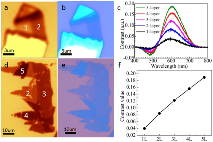
The white light contrast spectroscopy has been used for identification of layer numbers of atomically thin material such as graphene24 and TMDs25 through comparison of absorption of white light by different number of layers. Atomically thin TaSe2 samples deposited on 300 nm SiO2/Si substrate possesses linear relationship between white light absorption and layer number (see Fig. 1f ).
Figure 1. Layer number identification of atomically thin TaSe2 samples.
(a, d) White light contrast images and (b, e) Optical images of exfoliated TaSe2 samples with layer number ranging from 1 to 5. (c) White light contrast spectra and (f) extracted contrast values of different number of layers.
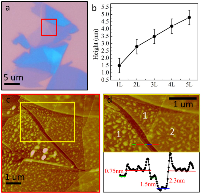
AFM measurements done in a tapping mode reveals high concentration of surface adsorbents and impurities in thin TaSe2 samples (Fig. 2c). According to the first principle calculations, thickness of single layer TaSe2 is expected to be around 0.65 ± 0.05 nm which is in good agreement with our AFM measurements26,27. The AFM height profile measured at the step of single layer TaSe2 sitting on TaSe2 crystal shows ~0.75 nm thickness which is consistent with the theoretical value28. However, the thickness readings of the single layer TaSe2 directly on the SiO2/Si substrate range from 1 nm to 1.5 nm which can be attributed to the large surface roughness of the substrate, adsorbents and impurities between substrate and the TaSe2 layer (Fig. 2d)29.
Figure 2. Layer number identification with AFM.
(a) Optical image of single layer and bilayer TaSe2 (b) heights measured by AFM of samples with different layer numbers (c) AFM image of the area within red square in (a). (d) AFM image (yellow squared area in b) and cross section profile of single layer (green line), bilayer (red line) TaSe2 samples on Si/SiO2 (blue line) substrate.
Identification of layer numbers of thin samples by AFM can be challenging especially if samples have been exposed to ambient air for a long time. On the other hand, white light contrast imaging gives us very precise values for number of layers even for weeks-old samples. Therefore, we conclude that contrast spectroscopy is more reliable and time-efficient methods for identifying number of layers. Recently, Gomez et al. published first article for fast identification of TaSe2 samples using contrast spectroscopy29. However thinnest sample they achieved by exfoliation is 5 layers in thickness.
Raman spectroscopy
In normal (metallic) phase, 2H-TaSe2 has crystal structure of hexagonal  symmetry. For one-phonon processes, unit cell has following vibrational modes:
Among them, A1g, E1g,  and
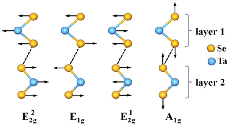
and  are Raman active modes (Fig. 3)22.
Figure 3. Vibrational modes for one-phonon processes.
A single layer structure corresponds to a sheet of Ta atoms sandwiched between two sheets of Se atoms (trilayer). The bulk 2H polytype contains two trilayers per unit cell.
From previous Raman measurements on bulk 2H-TaSe2, in backscattering Raman configuration, observable Raman peaks are (i) A1g - out of plane vibrational mode at 235 cm−1, (ii) in plane vibrations  at 208 cm−1 and
  - also known as rigid layer mode with the low energy at around 23 cm−1 and (iii) very broad second-order peak due to two-phonon process at around ~140 cm−1,
22. For this crystal symmetry, E1g vibrational mode is forbidden in backscattering Raman configuration30. From previous studies of bulk 2H-TaSe2 in non-backscattering Raman configuration, the E1g is observed at 137 cm−1,
31. The two-phonon Raman process can be described as either (i) creation or destruction of two phonons or (ii) simultaneous creation of one-phonon with destruction of another phonon. The second-order Raman peak is related to two-phonon density of states. The intensity of this peak at certain frequency ω depends on density of states of phonon pairs with frequency difference or sum equal to ω. Hence, the second-order Raman peak is a broad peak that arises from overlapped sharp peaks31,32.
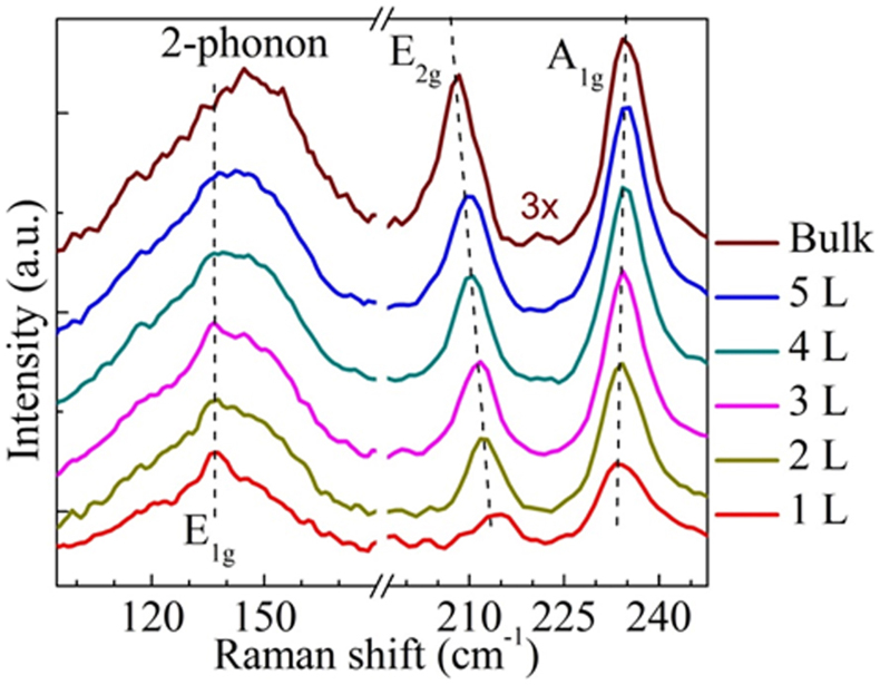
Figure 4 shows Raman spectra of TaSe2 samples supported on the 300 nm SiO2/Si substrate with thicknesses varying from single layer to bulk obtained in backscattering configuration. There are three prominent Raman features, which are A1g, E2g and 2-phonon modes for TaSe2 samples from single layer to bulk. Moreover, the E1g mode which is usually forbidden in backscattering Raman configuration was observed in the thin (less than 4 layers) TaSe2 samples. To our best effort, E1g peak was not observable in bulk or thin samples of more than 3 layers in thickness. It can be seen from Fig. 4 that the intensity of the E1g mode increases with decreasing number of layers. The reasons that E1g peak of thicker layers does not appear as clearly as it in thin layers could be due to (i) the second order Raman peak intensity increased with the number of layers, which may “suppress” the very weak E1g peak; (ii) the interaction of thicker layers and substrate could be dramatically weaker comparing to the case for very thin layers, this may further weaken the E1g intensity.
Figure 4. Raman spectra of TaSe2 samples, ranging from single layer to bulk in room temperature (in backscattering Raman configuration).
As number of layers decrease, the E2g and the A1g peaks approach each other. The E1g peak is easily observed at 137 cm−1 for samples below 4 layers in thickness.
Like MoS2, A1g and E2g peaks approach each other as number of layers decreases. Although the red-shift of the A1g peak is barely observable, nevertheless, a shift within ~1 cm−1 can be detected once the peaks are fit with Lorenz function. From bulk to single layer, the E2g mode shows a blue-shift of 6.5 cm−1. These shifts are mainly attributed to: (i) the decrease of the force constant resulted from the weakening of the interlayer Van der Waals force between layers for the A1g mode33; and (ii) the structure changes or long-range coulombic interlayer interactions for the E2g mode, when the number of layers decreases34.
To elucidate the dependence of the Raman features as a functional of the number of layers, the A1g, the E2g and the two-phonon peaks are fitted by Lorentz function and the fitting results are plotted in Fig. 5. Similar to MoS234, the energy difference of the A1g and the E2g is the smallest for the single layer, however, increment for this energy difference decreases with increasing layer number (Fig. 5a). The intensity increases with increasing number of layers and reaches a maximum value at certain number of layers (above 5 layers), then declines towards bulk value (Fig. 5c). This behavior is attributed to optical interference effect between thin layers and SiO2/Si substrate12. On the other hand, the relative intensity of the E2g mode to the A1g mode decreases more rapidly with decreasing number of layers (Fig. 5b). Observation of these associations between different layers could be another reliable way to identify the number of layers of thin TaSe2 samples.
Figure 5. Identification of number of layers by fitted Raman features.
(a) Energy difference between the A1g and the E2g modes saturates to bulk value in inversely exponential manner (b) relative intensity ratio of the E2g peak to the A1g peak in Raman spectrum shows linear relationship with increasing layer number (c) Signal-to-noise ratio of Raman spectrum improves with increasing layer number due to interference enhancement and starts to decline towards bulk value after passing through maximum point at certain layer number.
As noticed in Figure 4, the intensity of the E1g mode increases with decreasing number of layers. To further investigate the origin of this anomaly, we performed Raman measurements on suspended tri-layer TaSe2 samples because the signal-to-noise ratio of suspended tri-layer TaSe2 is acceptable for data analysis as the Raman signal of the suspended samples is considerable weaker than that of the supported samples. The temperature-dependent Raman spectra of supported 3-layer TaSe2 (Supplementary Fig. S1b) and suspended 3-layer TaSe2 (Supplementary Fig. S1c) are from the same sample as illustrated in the optical image of Supplementary Figure S1a measured under the same condition. It can be seen from this figure that for the supported sample, the E1g peak becomes more and more pronounced with decrease of the temperature because the noise and the background of the 2-phonon peak is minimized at low temperature. And the strength of the E1g Raman peak of the supported sample is comparable (in many cases stronger than) to that of the E2g peak. However, even at low temperatures, we did not observe any peak at around the location of the E1g peak which is comparable to the E2g peak. Therefore, we conclude that observation of the forbidden E1g mode in the supported thin TaSe2 samples might be due to the broken symmetry originating from the interaction with SiO2/Si substrate. Similar feature, appearance of new Raman inactive peaks due to symmetry breaking has been also observed in few quintuples of thin layered topological insulators35,36.
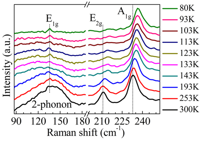
As mentioned before, 2H-TaSe2 in bulk has CDW phase transition at low temperatures within liquid nitrogen temperature region22. To investigate the CDW-influenced Raman scattering response together with the Raman feature evolutions with temperature, we performed the temperature-dependent Raman measurements on TaSe2 samples from single layer to bulk. Figure 6 shows representative temperature-dependent Raman spectra of bilayer TaSe2 sample in the temperature range of 80 K to 300 K. It can be seen that both the A1g and the E2g modes blue shift with decreasing temperature. Moreover, in our low temperature measurements, it is noticed that the intensities of the E2g mode and the broad two-phonon peak decline with decreasing temperature. Therefore, for thin layers, at temperatures below 120 K, the fitting results of these two peaks have large error bar in values due to the deteriorated signal-to-noise ratio. In contrast, the intensity of the forbidden E1g mode increases with decreasing temperatures. This may be explained as (i) declining background signal from the two-phonon process that enhances the visibility of this peak and (ii) strain induced effects due to difference in thermal expansion coefficients of substrate and thin films37,38.
Figure 6. In-situ low temperature micro-Raman spectra of bilayer TaSe2 sample.
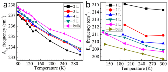
The results of our temperature-dependent Raman measurements on TaSe2 samples from single layer to bulk are summarized in Figure 7. It clearly shows that the energy of both the A1g and the E2g modes increases with decreasing temperatures. Phonon softening with increasing temperature or vice versa is a common behavior, just like in MoS239 and graphene40. This effect can be also observed through laser heating at different laser powers (see Supplementary Fig. S2). Temperature-dependent-shift in phonon energy is related to anharmonic terms in the lattice potential energy. This shift in one-phonon modes depends on anharmonic coupling of the phonons and the thermal expansion of the crystal41. In addition, in the case of TaSe2, energy of the A1g and the E2g modes is also related to electronic susceptibility. CDW phase transition is accompanied by increase in electronic susceptibility which can be observed through relatively sudden stiffening of phonons below critical phase transition temperature (~123 K). And it is observed in bulk that this sudden stiffening is more prominent for the E2g mode than the A1g42,22. However, in our measurements, as can be seen from Figure 6, we cannot observe this sudden stiffening for the E2g because at temperatures below 150 K, E2g peak intensity decreases dramatically and therefore the fitting results of the E2g peak have large error bar in values due to the poor signal–to-noise ratio.
Figure 7. Layer dependent behavior of the A1g (a) and the E2g (b) modes at low temperatures.
The second-order Raman peak is a very unique optical feature of CDW materials like TaSe2 and carries rich physics. The Kohn anomaly is an anomaly in the dispersion curve of a phonon branch in a metal. As discussed earlier, the second-order broad Raman peak arises from two-phonon scattering process involving longitudinal acoustic (LA) phonons43,44. The LA phonons in 2H-TMD compounds exhibit a Kohn anomaly which results in high two-phonon density of states. The presence of a Kohn anomaly in a LA mode is due to Fermi surface nesting and strong electron-phonon coupling required for a CDW transition8.
Bulk TaSe2 has Pierls phase transition from metallic to ICDW phase at ~123 K and another transition into CCDW phase at ~90 K. In CCDW phase, 2H-TaSe2 has superlattice with 3a x 3a x c unit cell and the same hexagonal  symmetry. Below 90 K, four new Raman modes appear at energy range lower than 85 cm−1 in Raman spectrum which are directly associated with the creation of the CDW superlattice over underlying crystal lattice45. However, in our measurements, we could not observe these peaks and the
  rigid-layer mode, because our Rayleigh rejection filter has a cut-off point above 80 cm−1. From previous work done on Raman study of bulk TaSe2 in CDW phase, we know that on approach to transition temperature from normal to ICDW phase the broad peak due to two-phonon process broadens, exhibits a red-shift and is significantly reduced in intensity46,31,22.
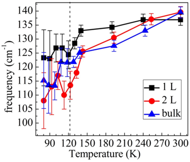
As depicted in Figure 8, an overall softening of the 2-phonon peak can be clearly seen for single, bilayer and bulk TaSe2. More importantly, a sudden drop of the frequency of this two-phonon mode appear for all the three samples at ~120 K, close to the critical temperature for the phase transition from normal metallic to ICDW as previously reported22. This clearly demonstrates the existence of the ICDW phase in the atomic thin layers of TaSe2. Recent theoretical studies suggest that CDW distortion for TaSe2 might be stronger in thin layers than in bulk, however, critical transition temperature should be similar to bulk28. Layer dependent critical transition temperatures cannot be determined in this work due to severely diminished intensity of broad Raman peak which results in large error of values during peak fitting. More details including the low wavenumber modes will be exploited and reported in our future works.
Figure 8. Observation of phase transition through sudden softening of two-phonon peaks.
In bulk samples, upon ICDW phase transition temperatures, the broad peak due to 2-phonon process broadens, softens in energy and intensity also decreases (black dashed line represents ICDW phase transition point for bulk at ~123 K). This broad peak is fitted by Lorenz function to obtain frequency corresponding to the center of the peak (the data below 120 K has huge error due to severely diminished Raman signal). As temperature approaches to Peierls phase transition point, 2-phonon peak for single layer and bilayer samples softens similar to bulk sample.
Discussion
We have demonstrated for the first time, the mechanical exfoliation of single layer TaSe2 and layer number identification for thin samples using well-known AFM measurement and white light contrast spectroscopy techniques. Room temperature Raman measurements for atomic thin layers of TaSe2 reveal resembling features to MoS2 and other layered TMDs. We have additionally observed the forbidden E1g peak in backscattering configuration in all thin layers, particularly below 4-layered samples, which is probably due to the symmetry breaking induced by the interaction between thin TaSe2 layers and substrate. Low temperature Raman measurements show similar properties for thin layered samples to the previous bulk studies of TaSe2 and indicate the existence of ICDW phase in the atomic thin layers of 2H-TaSe2. The low Raman signal-to-noise ratio at low temperatures may be an obstacle for detailed “error-free” analysis of the data. Meanwhile, a narrow band Notch filer could benefit to the direct observation of low-wavenumber peaks related to the CDW superlattice.
Methods
Sample fabrication
Samples are isolated by scotch-tape technique and deposited on 300 nm SiO2/Si substrates. For suspended samples these substrates were chemically etched with grid of holes ~3 μm in diameter. Then suitable samples are searched and located under an optical microscope.
Layer number identification
Isolated samples are mapped by AFM in tapping mode and white light contrast spectroscopy. We conducted the white light contrast spectroscopy using WITEC CRM200 system with a 150 lines/mm grating and a 100x objective lens.
Raman spectroscopy
Micro-Raman measurements have been conducted by a Renishaw system with 50x, 80x long working distance objective lens and a 2400 lines/mm grating under 532 nm laser excitation. The laser power is regulated below 3 mW and the laser spot size is ~ 1.5 μm. For room and low temperature Raman measurements, a temperature-controlled evacuated chamber cooled by liquid nitrogen is used for preventing the potential oxidation and local heating of the TaSe2 samples under laser irradiation. The TaSe2 samples are very easily burned if Raman measurements carried out in oxygen-rich ambient. Detailed description of laser burning related effects during Raman measurements can be found in the Supplementary Information (see Supplementary Fig. S2).
Author Contributions
T.Y. and C.X.C. initialled the project, conceived and designed the experiments; P.H. conducted Raman measurements, analyzed the data; C.Y.Q. performed sample exfoliation and preparation of suspended samples; All author contributed to contrast spectroscopy and AFM measurements, and discussed the results, commented on the manuscript.
Supplementary Material
Supplementary Information
Acknowledgments
The work described here is supported by the Singapore National Research Foundation under Award No. NRF-RF2010-07 and MOE Tier 2 MOE2012-T2-2-049.
References
- Wang Q. H., Kalantar-Zadeh K., Kis A., Coleman J. N. & Strano M. S. Electronics and optoelectronics of two-dimensional transition metal dichalcogenides. Nature Nanotechnology 7, 699–712 (2012). [DOI] [PubMed] [Google Scholar]
- Ataca C., Sahin H. & Ciraci S. Stable, Single-Layer MX 2 Transition-Metal Oxides and Dichalcogenides in a Honeycomb-Like Structure. The journal of Physical Chemistry (2012). [Google Scholar]
- Wilson J. A., Di Salvo F. J. & Mahajan S. Charge-Density Waves in Metallic, Layered, Transition-Metal Dichalcogenides. Physical review letters 32, (1974). [Google Scholar]
- Sipos B. et al. From Mott state to superconductivity in 1T-TaS2. Nature materials 7, 960–5 (2008). [DOI] [PubMed] [Google Scholar]
- Castro Neto a. H. Charge Density Wave, Superconductivity, and Anomalous Metallic Behavior in 2D Transition Metal Dichalcogenides. Physical Review Letters 86, 4382–4385 (2001). [DOI] [PubMed] [Google Scholar]
- Nagaosa N. & Hanamura E. Microscopic theory of the Raman and infrared spectra of transition-metal dichlcogenides in the charge-density-wave state. Physical Review B 29, (1984). [Google Scholar]
- Galvis J. a. et al. Scanning tunneling measurements of layers of superconducting 2H-TaSe2: Evidence for a zero-bias anomaly in single layers. Physical Review B 87, 094502 (2013). [Google Scholar]
- Moncton D. E., Axe J. D. & Disalvo F. J. Study of Superlattice Formation in 2H-NbSe2 and 2H-TaSe2 by Neutron Scattering. Physical Review Letters 34, 734–737 (1975). [Google Scholar]
- Johari P. & Shenoy V. B. Tunable dielectric properties of transition metal dichalcogenides. ACS nano 5, 5903–8 (2011). [DOI] [PubMed] [Google Scholar]
- Shen D. et al. Novel Mechanism of a Charge Density Wave in a Transition Metal Dichalcogenide. Physical Review Letters 99, 216404 (2007). [DOI] [PubMed] [Google Scholar]
- Editorial, Graphene is not alone. Nature Nanotechnology 7, 683 (2012). [DOI] [PubMed] [Google Scholar]
- Li S.-L. et al. Quantitative Raman spectrum and reliable thickness identification for atomic layers on insulating substrates. ACS nano 6, 7381–8 (2012). [DOI] [PubMed] [Google Scholar]
- Cong C. et al. Raman Characterization of ABA- and ABC-Stacked Trilayer Graphene. Acs Nano 5, 1600 (2011). [DOI] [PubMed] [Google Scholar]
- Lui C. H. et al. Imaging stacking order in few-layer graphene. Nano letters 11, 164–9 (2011). [DOI] [PubMed] [Google Scholar]
- Chunxiao C., Kun L., Xi Xiang Z. & Ting Y. Visualization of arrangements of carbon atoms in graphene layers by Raman mapping and atomic-resolution TEM. Sci. Rep. 3, 1195 (2013). [DOI] [PMC free article] [PubMed] [Google Scholar]
- Chunxiao C., Yu T. & Wang H. M. Raman study on the G mode of graphene for determination of edge orientation. ACS Nano 4, 3175 (2010). [DOI] [PubMed] [Google Scholar]
- Lv R. et al. Nitrogen-doped graphene: beyond single substitution and enhanced molecular sensing. Sci. Rep. 2, 586 (2012). [DOI] [PMC free article] [PubMed] [Google Scholar]
- Lee J. E., Ahn G., Shim J., Lee Y. S. & Ryu S. Optical separation of mechanical strain from charge doping in graphene. Nature communications 3, 1024 (2012). [DOI] [PubMed] [Google Scholar]
- Ni Z. et al. Uniaxial strain on graphene: Raman spectroscoy study and bandgap opening. ACS Nano 2, 2301 (2008). [DOI] [PubMed] [Google Scholar]
- Ferrari a. C. et al. Raman Spectrum of Graphene and Graphene Layers. Physical Review Letters 97, 1–4 (2006). [DOI] [PubMed] [Google Scholar]
- Li H. et al. Mechanical Exfoliation and Characterization of Single- and Few-Layer Nanosheets of WSe2, TaS2, and TaSe2. Small (Weinheim an der Bergstrasse, Germany) 1–10 (2012). 10.1002/smll.201202919. [DOI] [PubMed] [Google Scholar]
- Sugai S. & Murase K. Generelized electronic susceptibility and charge density waves in 2H-TaSe2 by Raman scattering. Physical Review B 25, (1982). [Google Scholar]
- Rossnagel K. On the origin of charge-density waves in select layered transition-metal dichalcogenides. Journal of physics. Condensed matter: an Institute of Physics journal 23, 213001 (2011). [DOI] [PubMed] [Google Scholar]
- Ni Z. H. et al. Graphene thickness determination using reflection and contrast spectroscopy. Nano letters 7, 2758–63 (2007). [DOI] [PubMed] [Google Scholar]
- Castellanos-Gomez a., Agraït N. & Rubio-Bollinger G. Optical identification of atomically thin dichalcogenide crystals. Applied Physics Letters 96, 213116 (2010). [Google Scholar]
- Ding Y. et al. First principles study of structural, vibrational and electronic properties of graphene-like MX2 (M = Mo, Nb, W, Ta; X = S, Se, Te) monolayers. Physica B: Condensed Matter 406, 2254–2260 (2011). [Google Scholar]
- Kuchinskii E. Z., Nekrasov I. a. & Sadovskii M. V. Electronic structure of two-dimensional hexagonal diselenides: Charge density waves and pseudogap behavior. Journal of Experimental and Theoretical Physics 114, 671–680 (2012). [Google Scholar]
- Ge Y. & Liu A. Effect of dimensionality and spin-orbit coupling on charge-density-wave transition in 2H-TaSe_{2}. Physical Review B 86, 104101 (2012). [Google Scholar]
- Castellanos-gomez A. et al. Fast and reliable identification of atomically thin layers of TaSe 2 crystals. Nano Research (2013). 10.1007/s12274. [Google Scholar]
- Zhao W. et al. Lattice dynamics in mono- and few-layer sheets of WS 2 and WSe 2, arXiv:1304.0911v1. (2013). [DOI] [PubMed]
- A. Holy J., V. Klein M., McMillan W. L. & Meyer S. F. Raman-Active Lattice Vibrations of Commensurate Superlattice in 2H-TaSe2. Physical Rewiev Letters 37, 1–4 (1976). [Google Scholar]
- Sugai S. Lattice Vibrations in the Charge-Density-Wave States of Layered Transition Metal Dichalcogenides. Physica Status Solidi (B) 129, 13–39 (1985). [Google Scholar]
- Li H. et al. From Bulk to Monolayer MoS2: Evolution of Raman Scattering. Advanced Functional Materials 22, 1385–1390 (2012). [Google Scholar]
- Lee C. et al. Anomalous Lattice Vibrations of Single-and Few-Layer MoS2. ASC Nano 4, 2695–2700 (2010). [DOI] [PubMed] [Google Scholar]
- Teweldebrhan D., Goyal V. & Balandin A. a. Exfoliation and characterization of bismuth telluride atomic quintuples and quasi-two-dimensional crystals. Nano letters 10, 1209–18 (2010). [DOI] [PubMed] [Google Scholar]
- Zhang J. et al. Raman Spectroscopy of Few-Quintuple Layer Topological Insulator Bi2Se3 Nanoplatelets. Nano letters 2407–2414 (2011). [DOI] [PubMed] [Google Scholar]
- Tada H. et al. Thermal expansion coefficient of polycrystalline silicon and silicon dioxide thin films at high temperatures. Applied Physics Letters 87, 61–68 (2000). [Google Scholar]
- Maclean D. & Jericho M. H. Effect of the charge-density-wave transition on the thermal expansion of 2H-TaSe2, NbSe3, and o-TaS3. Physical Review B 47, (1993). [DOI] [PubMed] [Google Scholar]
- Najmaei S., Liu Z., Ajayan P. M. & Lou J. Thermal effects on the characteristic Raman spectrum of molybdenum disulfide (MoS2) of varying thicknesses. Applied Physics Letters 100, 013106 (2012). [Google Scholar]
- Calizo I., Balandin a. a., Bao W., Miao F. & Lau C. N. Temperature dependence of the Raman spectra of graphene and graphene multilayers. Nano letters 7, 2645–9 (2007). [DOI] [PubMed] [Google Scholar]
- Postmus C., Ferraro J. R. & Mitra S. S. Pressure Dependence of Infrared Eigenfrequencies of KCl and KBr. Physical Review 174, (1968). [Google Scholar]
- Tsang J. C., Smith J. E. & Shafer M. W. Effect of charge density wave fluctuations on the frequencies of optic phonon in 2H-TaSe2 and -NbSe2. Solid State Communications 27, 145–149 (1978). [Google Scholar]
- Klein M. V. Theory of Raman scattering from charge-density-wave phonons. Physical Review B 25, 7192–7208 (1982). [Google Scholar]
- Tsang J. C., Smith J. E., Shafer M. W. & Meyer S. F. Raman Spectroscopy of charge-density-wave state in 1T- and 2H-TaSe2. Physical Review B 16, (1977). [Google Scholar]
- Sugai S., Murase K., Uchida S. & Tanaka S. Comparison of the soft modes in Tantalum Dichalcogenides. Physica 105B (1981). [Google Scholar]
- Smith J. E., Tsang J. C. & Shafer M. W. Raman spectra of several layer compounds with charge density waves. Solid State Communications 19, 283–286 (1976). [Google Scholar]
- Ge Y. & Liu A. Effect of dimensionality and spin-orbit coupling on charge-density-wave transition in 2H-TaSe_{2}. Physical Review B 86, 104101 (2012). [Google Scholar]
Associated Data
This section collects any data citations, data availability statements, or supplementary materials included in this article.
Supplementary Materials
Supplementary Information


